Document Outline
- COVER
- Description
- Features
- Ordering Information
- Part Number
- Pin Configurations
- Electrical Specifications
- Absolute Maximum Ratings
- Operating Temperature Condition
- Recommended DC Operating Conditions
- DC Characteristics 1
- AC Timing for IDD Test Conditions
- DC Characteristics 2
- DC Characteristics 3
- ODT DC Electrical Characteristics
- OCD Default Characteristics
- Pin Capacitance
- AC Characteristics
- ODT AC Electrical Characteristics
- AC Input Test Conditions
- Block Diagram
- Pin Function
- Command Operation
- Command Truth Table
- CKE Truth Table
- Function Truth Table
- Simplified State Diagram
- Operation of DDR2 SDRAM
- Power On and Initialization
- Power-Up and Initialization Sequence
- Programming the Mode Register and Extended Mode Registers
- DDR2 SDRAM Mode Register Set [MRS]
- DDR2 SDRAM Extended Mode Registers Set [EMRS]
- Off-Chip Driver (OCD) Impedance Adjustment
- ODT(On Die Termination)
- Bank Activate Command
- Read and Write Access Modes
- Posted /CAS
- Burst Mode Operation
- Burst Read Command
- Burst Write Command
- Write Data Mask
- Precharge Command
- Burst Read Operation Followed by Precharge
- Burst Write Followed by Precharge
- Auto-Precharge Operation
- Burst Read with Auto Precharge
- Burst Write with Auto-Precharge
- Refresh Requirements
- Automatic Refresh Command
- Self Refresh Command
- Power-Down
- Asynchronous CKE Low Event
- Input Clock Frequency Change during Precharge Power Down
- Burst Interruption
- No Operation Command
- Deselect Command
- Package Drawing
- 64-ball FBGA (uBGA)
- 84-ball FBGA (uBGA)
- Recommended Soldering Conditions

Document No. E0323E90 (Ver. 9.0)
Date Published September 2005 (K) Japan
Printed in Japan
URL: http://www.elpida.com
Elpida Memory, Inc. 2002-2005
DATA SHEET
512M bits DDR2 SDRAM
EDE5104ABSE (128M words
◊
4 bits)
EDE5108ABSE (64M words
◊
8 bits)
EDE5116ABSE (32M words
◊
16 bits)
Description
The EDE5104ABSE is a 512M bits DDR2 SDRAM
organized as 33,554,432 words
◊
4 bits
◊
4 banks.
The EDE5108ABSE is a 512M bits DDR2 SDRAM
organized as 16,777,216 words
◊
8 bits
◊
4 banks.
They are packaged in 64-ball FBGA (
µ
BGA
) package.
The EDE5116ABSE is a 512M bits DDR2 SDRAM
organized as 8,388,608 words
◊
16 bits
◊
4 banks.
It is packaged in 84-ball FBGA (
µ
BGA) package.
Features
∑
Power supply: VDD, VDDQ
=
1.8V
±
0.1V
∑
Double-data-rate architecture: two data transfers per
clock cycle
∑
Bi-directional, differential data strobe (DQS and
/DQS) is transmitted/received with data, to be used in
capturing data at the receiver
∑
DQS is edge aligned with data for READs: center-
aligned with data for WRITEs
∑
Differential clock inputs (CK and /CK)
∑
DLL aligns DQ and DQS transitions with CK
transitions
∑
Commands entered on each positive CK edge: data
and data mask referenced to both edges of DQS
∑
Four internal banks for concurrent operation
∑
Data mask (DM) for write data
∑
Burst lengths: 4, 8
∑
/CAS Latency (CL): 3, 4, 5
∑
Auto precharge operation for each burst access
∑
Auto refresh and self refresh modes
∑
7.8
µ
s average periodic refresh interval
∑
SSTL_18 compatible I/O
∑
Posted CAS by programmable additive latency for
better command and data bus efficiency
∑
Off-Chip-Driver Impedance Adjustment and On-Die-
Termination for better signal quality
∑
Programmable RDQS, /RDQS output for making
◊
8
organization compatible to
◊
4 organization
∑
/DQS, (/RDQS) can be disabled for single-ended
Data Strobe operation.
∑
FBGA (
µ
BGA) package with lead free solder
(Sn-Ag-Cu)
RoHS compliant
EDE5104ABSE, EDE5108ABSE, EDE5116ABSE
Data Sheet E0323E90 (Ver. 9.0)
2
Ordering Information
Part number
Mask
version
Organization
(words
◊
bits)
Internal
Banks
Speed bin
(CL-tRCD-tRP)
Package
EDE5104ABSE-5C-E
EDE5104ABSE-4A-E
B 128M
◊
4
4
DDR2-533 (4-4-4)
DDR2-400 (3-3-3)
64-ball FBGA (
µ
BGA)
EDE5108ABSE-5C-E
EDE5108ABSE-4A-E
64M
◊
8
DDR2-533 (4-4-4)
DDR2-400 (3-3-3)
EDE5116ABSE-5C-E
EDE5116ABSE-4A-E
32M
◊
16
DDR2-533 (4-4-4)
DDR2-400 (3-3-3)
84-ball FBGA (
µ
BGA)
Part Number
Elpida Memory
Density / Bank
51: 512M /4 banks
Bit Organization
04: x4
08: x8
16: x16
Voltage, Interface
A: 1.8V, SSTL_18
Die Rev.
Package
SE: FBGA (
µ
BGA with back cover)
Speed
5C: DDR2-533 (4-4-4)
4A: DDR2-400 (3-3-3)
Product Code
E: DDR2
Type
D: Monolithic Device
E D E 51 04 A B SE - 5C - E
Environment code
E: Lead Free

EDE5104ABSE, EDE5108ABSE, EDE5116ABSE
Data Sheet E0323E90 (Ver. 9.0)
3
Pin Configurations
/xxx indicates active low signal.
VDD
1
DQ6
(NC)*
VDDQ
DQ4
(NC)*
VDDL
VSS
VDD
2
NU/ /RDQS
(NC)*
VSSQ
DQ1
VSSQ
VREF
CKE
BA0
A10
A3
A7
A12
3
VSS
DM/RDQS
(DM)*
VDDQ
DQ3
VSS
/WE
BA1
A1
A5
A9
NC
7
VSSQ
DQS
VDDQ
DQ2
VSSDL
/RAS
/CAS
A2
A6
A11
NC
8
/DQS
VSSQ
DQ0
VSSQ
CK
/CK
/CS
A0
A4
A8
A13
9
VDDQ
DQ7
(NC)*
VDDQ
DQ5
(NC)*
VDD
VDD
VSS
(Top view)
64-ball FBGA (
µ
BGA)
Note: ( )* marked pins are for
◊
4 organization.
NC
ODT
(
◊
8,
◊
4 organization)
A
B
C
D
E
F
G
H
J
K
L
VDD
1
VDDQ
VDD
VDDL
2
VSSQ
UDM
DQ14
DQ9
VSSQ
DQ12
NC
VREF
3
VSS
NC
VDDQ
DQ11
VSS
CKE
/WE
VSS
7
VSSQ
UDQS
VDDQ
DQ10
VSSQ
/RAS
8
/UDQS
VSSQ
DQ15
DQ8
VSSQ
DQ13
/LDQS
/CK
M
N
P
R
VDD
A12
NC
NC
NC
9
VDDQ
VDDQ
DQ6
DQ4
VSSQ
DQ1
VDDQ
VSSQ
LDM
VDDQ
DQ3
LDQS
VDDQ
VSSQ
DQ0
VDDQ
DQ2
VSSQ
DQ5
DQ7
VDDQ
VSSDL
CK
VDD
VSS
A10
A3
A7
A1
A5
A9
A2
A6
A11
A0
A4
A8
VDD
VSS
(Top view)
84-ball FBGA (
µ
BGA)
BA0
BA1
/CAS
/CS
NC
ODT
(
◊
16 organization)
NC
NC
A
B
C
D
E
F
G
H
J
K
L
M
N
P
R
NC
NC
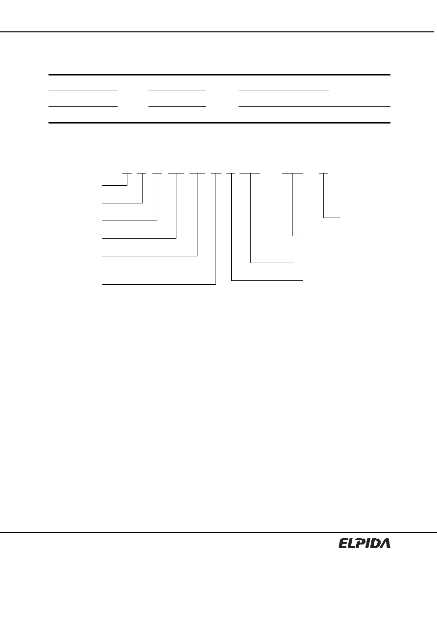
Pin name
Function
Pin name
Function
A0 to A13
Address inputs
ODT
ODT control
BA0, BA1
Bank select
VDD
Supply voltage for internal circuit
DQ0 to DQ15
Data input/output
VSS
Ground for internal circuit
DQS, /DQS
UDQS, /UDQS
LDQS, /LDQS
Differential data strobe
VDDQ
Supply voltage for DQ circuit
RDQS, /RDQS
Differential data strobe for read
VSSQ
Ground for DQ circuit
/CS
Chip select
VREF
Input reference voltage
/RAS, /CAS, /WE
Command input
VDDL
Supply voltage for DLL circuit
CKE
Clock enable
VSSDL
Ground for DLL circuit
CK, /CK
Differential clock input
NC*
1
No
connection
DM, UDM, LDM
Write data mask
NU*
2
Not
usable
Notes: 1. Not internally connected with die.
2. Don't use other than reserved functions.
EDE5104ABSE, EDE5108ABSE, EDE5116ABSE
Data Sheet E0323E90 (Ver. 9.0)
4
CONTENTS
Description.....................................................................................................................................................1
Features.........................................................................................................................................................1
Ordering Information......................................................................................................................................2
Part Number ..................................................................................................................................................2
Pin Configurations .........................................................................................................................................3
Electrical Specifications.................................................................................................................................5
Block Diagram .............................................................................................................................................15
Pin Function.................................................................................................................................................16
Command Operation ...................................................................................................................................18
Simplified State Diagram .............................................................................................................................25
Operation of DDR2 SDRAM ........................................................................................................................26
Package Drawing ........................................................................................................................................62
Recommended Soldering Conditions..........................................................................................................64
EDE5104ABSE, EDE5108ABSE, EDE5116ABSE
Data Sheet E0323E90 (Ver. 9.0)
5
Electrical Specifications
Absolute Maximum Ratings
Parameter Symbol
Rating Unit
Notes
Power supply voltage
VDD
-
1.0 to +2.3
V
1
Power supply voltage for output
VDDQ
-
0.5 to +2.3
V
1
Input voltage
VIN
-
0.5 to +2.3
V
1
Output voltage
VOUT
-
0.5 to +2.3
V
1
Storage temperature
Tstg
-
55 to +100
∞
C 1,
2
Power dissipation
PD
1.0
W
1
Short circuit output current
IOUT
50
mA
1
Notes: 1. Stresses greater than those listed under Absolute Maximum Ratings may cause permanent damage to
the device. This is a stress rating only and functional operation of the device at these or any other
conditions above those indicated in the operational sections of this specification is not implied. Exposure
to absolute maximum rating conditions for extended periods may affect reliability.
2. Storage temperature is the case surface temperature on the center/top side of the DRAM.
Caution
Exposing the device to stress above those listed in Absolute Maximum Ratings could cause
permanent damage. The device is not meant to be operated under conditions outside the limits
described in the operational section of this specification. Exposure to Absolute Maximum Rating
conditions for extended periods may affect device reliability.
Operating Temperature Condition
Parameter Symbol
Rating Unit
Notes
Operating case temperature
TC
0 to +85
∞
C 1,
2
Notes: 1. Operating temperature is the case surface temperature on the center/top side of the DRAM.
2. The operation temperature range is the temperature where all DRAM specification will be supported. Out
side of this temperature range, even it is still within the limit of stress condition, some deviation on portion
of operation specification may be required.
During operation, the DRAM case temperature must be maintained between 0 to +85∞C under all other
specification parameters.