Document Outline
- COVER
- Description
- Features
- Pin Configurations
- Ordering Information
- Part Number
- Electrical Specifications
- Absolute Maximum Ratings
- Recommended Operating Conditions
- DC Characteristics 1
- DC Characteristics 2
- Pin Capacitance
- AC Characteristics
- Test Conditions
- Synchronous Characteristics
- Asynchronous Characteristics
- Pin Function
- Command Operation
- Truth Table
- Command Truth Table
- DQM Truth Table
- CKE Truth Table
- Function Truth Table
- Simplified State Diagram
- Initialization
- Programming Mode Registers
- Mode register
- Extended Mode Register
- Mode Register Definition
- Burst Length and Sequence
- Address Bits of Bank-Select and Precharge
- Operation of the Mobile RAM
- Precharge
- Auto Precharge
- Read /Write Command Interval
- Burst Termination
- Timing Waveforms
- AC Parameters for Read Timing with Manual Precharge
- AC Parameters for Read Timing with Auto Precharge
- AC Parameters for Write Timing
- Mode Register Set
- Extended Mode Register Set
- Power On Sequence
- /CS Function
- Clock Suspension during Burst Read
- Clock Suspension during Burst Write
- Power Down Mode and Clock Mask
- Auto Refresh
- Self Refresh (Entry and Exit)
- Deep Power Down Entry
- Deep Power Down Exit
- Random Column Read
- Random Column Write
- Random Row Read
- Random Row Write
- Read and Write
- Interleaved Column Read Cycle
- Interleaved Column Write Cycle
- Auto Precharge after Read Burst
- Auto Precharge after Write Burst
- Burst Write Operation
- Precharge Termination
- Package Drawing
- Recommended Soldering Conditions

Document No. E0196E30 (Ver. 3.0)
Date Published June 2002 (K) Japan
URL: http://www.elpida.com
Elpida Memory, Inc. 2001-2002
DATA SHEET
128M bits Mobile RAM
EDL1216AASA (8M words
◊
◊
◊
◊
16 bits)
Description
The EDL1216AA is a 128M bits Mobile RAM organized
as 2,097,152 words
◊
16 bits
◊
4 banks. The Mobile
RAM achieved low power consumption and high-speed
data transfer using the pipeline architecture. All inputs
and outputs are synchronized with the positive edge of
the clock.
This product is packaged in 54-ball FBGA (
µ
BGA
).
Features
∑
Low voltage power supply
VDD:
2.5V
±
0.2V
VDDQ: 1.8V
±
0.15V
∑
Wide temperature range (
-
25
∞
C to 85
∞
C)
∑
Programmable partial self refresh
∑
Programmable driver strength
∑
Programmable temperature compensated self refresh
(Option)
∑
Deep power down mode
∑
Small package (54-ball FBGA (
µ
BGA))
∑
Fully Synchronous Dynamic RAM, with all signals
referenced to a positive clock edge
∑
Pulsed interface
∑
Possible to assert random column address in every
cycle
∑
Quad internal banks controlled by BA0 and BA1
∑
Byte control by LDQM and UDQM
∑
Wrap sequence = Sequential/ Interleave
∑
/CAS latency (CL) = 2, 3
∑
Automatic precharge and controlled precharge
∑
Auto refresh and self refresh
∑ ◊
16 organization
∑
4,096 refresh cycles/64ms
∑
Burst termination by Burst stop command and
Precharge command
∑
FBGA(
µ
BGA) package is lead free solder (Sn-Ag-Cu)
Applications
Mobile cellular handsets, PDAs, wireless PDAs,
handheld PCs, home electronic appliances, and
information appliances, etc.
Pin Configurations
/xxx indicates active low signal.
VSS
1
A
B
C
D
E
F
G
H
J
2
3
4
5
6
7
8
9
DQ14
DQ12
DQ10
DQ8
UDQM
NC
A8
VSS
DQ15
DQ13
DQ11
DQ9
NC
CLK
A11
A7
A5
VSSQ
VDDQ
VSSQ
VDDQ
VSS
CKE
A9
A6
A4
VDDQ
VSSQ
VDDQ
VSSQ
VDD
/CAS
BA0
A0
A3
DQ0
DQ2
DQ4
DQ6
LDQM
/RAS
BA1
A1
A2
VDD
DQ1
DQ3
DQ5
DQ7
/WE
/CS
A10
VDD
(Top view)
A0 to A11
Address inputs
BA0, BA1
Bank select
DQ0 to DQ15
Data inputs/ outputs
CLK
Clock input
CKE
Clock enable
/CS
Chip select
/RAS
Row address strobe
/CAS
Column address strobe
/WE Write
enable
UDQM
Upper DQ mask enable
LDQM
Lower DQ mask enable
VDD Power
supply
VSS
Ground
VDDQ
Power supply for DQ
VSSQ
Ground for DQ
NC No
connection
54-ball FBGA ( BGA)

EDL1216AASA
Data Sheet E0196E30 (Ver. 3.0)
2
Ordering Information
Part number
Organization
(words
◊
bits)
Internal Banks
Clock frequency
MHz (max.)
/CAS latency
Package
EDL1216AASA-75-E
8M
◊
16
4
133
3
54-ball FBGA (
µ
BGA)
Part Number
Lead Free
Elpida Memory
Density / Bank
12: 128M / 4 banks
Bit Organization
16: x16
Voltage, Interface
A: VDD = 2.5V, VDDQ = 1.8V, LVCMOS
Die Rev.
Package
SA:
µ
BGA
Speed
75: 133MHz
Product Code
L: Mobile RAM
Type
D: Monolithic Device
E D L 12 16 A A SA - 75 - E

EDL1216AASA
Data Sheet E0196E30 (Ver. 3.0)
3
CONTENTS
Description .................................................................................................................................................... 1
Features ........................................................................................................................................................ 1
Applications ................................................................................................................................................... 1
Pin Configurations ......................................................................................................................................... 1
Ordering Information ..................................................................................................................................... 2
Electrical Specifications................................................................................................................................. 4
Pin Function .................................................................................................................................................. 9
Command Operation ................................................................................................................................... 10
Truth Table .................................................................................................................................................. 14
Simplified State Diagram............................................................................................................................. 19
Initialization.................................................................................................................................................. 20
Programming Mode Registers .................................................................................................................... 20
Address Bits of Bank-Select and Precharge ............................................................................................... 24
Operation of the Mobile RAM ...................................................................................................................... 25
Timing Waveforms ...................................................................................................................................... 33
Package Drawing ........................................................................................................................................ 56
Recommended Soldering Conditions.......................................................................................................... 57
Revision History .......................................................................................................................................... 60
EDL1216AASA
Data Sheet E0196E30 (Ver. 3.0)
4
Electrical Specifications
∑
All voltages are referenced to VSS (GND).
∑
After power up, wait more than 200
µ
s and then, execute Power on sequence and two Auto Refresh before proper
device operation is achieved.
Absolute Maximum Ratings
Parameter
Symbol
Rating
Unit
Note
Voltage on any pin relative to VSS
VT
≠0.5 to +3.6
V
Supply voltage relative to VSS
VDD, VDDQ
≠0.5 to +3.6
V
Short circuit output current
IOS
50
mA
Power dissipation
PD
1.0
W
Operating ambient temperature
TA
≠25 to +85
∞
C
Storage temperature
Tstg
≠55 to +125
∞
C
Caution
Exposing the device to stress above those listed in Absolute Maximum Ratings could cause
permanent damage. The device is not meant to be operated under conditions outside the limits
described in the operational section of this specification. Exposure to Absolute Maximum Rating
conditions for extended periods may affect device reliability.
Recommended Operating Conditions (TA = ≠25 to +85
∞
∞
∞
∞
C)
Parameter
Symbol
min.
typ.
max.
Unit
Notes
Supply voltage
VDD
2.3
2.5
2.7
V
VSS
0
0
0
V
DQ Supply voltage
VDDQ
1.65
1.8
1.95
V
Input high voltage
VIH
0.8
◊
VDDQ
VDDQ + 0.3*
1
V
Input low voltage
VIL
≠0.3*
2
0.3
V
Notes: 1. VIH (max.) = VDDQ + 1.5V (pulse width 5ns).
2. VIL (min.) = ≠1.5V (pulse width 5ns).

EDL1216AASA
Data Sheet E0196E30 (Ver. 3.0)
5
DC Characteristics (TA = ≠25 to +85
∞
∞
∞
∞
C, VDD = 2.5V ± 0.2V, VDDQ = 1.8V ± 0.15V, VSS, VSSQ = 0V)
Parameter
/CAS latency
Symbol
Grade
max.
Unit
Test condition
Notes
Operating current
(CL = 2)
IDD1
65
mA
1
(CL = 3)
IDD1
65
mA
Burst length = 1
tRC
tRC min., IO = 0mA,
One bank active
Standby current in power down
IDD2P
1
mA
CKE
VIL max., tCK = 15ns
Standby current in power down
(input signal stable)
IDD2PS
0.6
mA
CKE
VIL max., tCK =
Standby current in non power
down
IDD2N
5.5
mA
CKE
VIH min., tCK = 15ns,
/CS
VIH min.,
Input signals are changed one
time during 30ns.
Standby current in non power
down (input signal stable)
IDD2NS
2
mA
CKE
VIH min., tCK =
,
Input signals are stable.
Active standby current in power
down
IDD3P
1.5
mA
CKE
VIL max., tCK = 15ns
Active standby current in power
down (input signal stable)
IDD3PS
1
mA
CKE
VIL max., tCK =
Active standby current in non
power down
IDD3N
17
mA
CKE
VIH min., tCK = 15 ns,
/CS
VIH min.,
Input signals are changed one
time during 30ns.
Active standby current in non
power down (input signal stable)
IDD3NS
12
mA
CKE
VIH min., tCK =
,
Input signals are stable.
Burst operating current
(CL = 2)
IDD4
60
mA
tCK
tCK min.,
IOUT = 0mA, All banks active
2
(CL = 3)
IDD4
80
mA
Refresh current
(CL = 2)
IDD5
155
mA
tRC
tRC min.
3
(CL = 3)
IDD5
155
mA
Self refresh current
PASR="000" (Full)
IDD6
0.35
mA
TCSR="00" (Ts*
4
70∞C)
PASR="001" (2BK)
0.25
mA
CKE
0.2V
PASR="010" (1BK)
0.18
mA
PASR="101" (1/2 BK)
0.12
mA
PASR="110" (1/4 BK)
0.09
mA
PASR="000" (Full)
IDD6
0.20
mA
TCSR="01" (Ts*
4
45∞C)
PASR="001" (2BK)
0.15
mA
CKE
0.2V
PASR="010" (1BK)
0.10
mA
PASR="101" (1/2 BK)
0.08
mA
PASR="110" (1/4 BK)
0.07
mA
PASR="000" (Full)
IDD6
0.60
mA
TCSR="11" (Ts*
4
85∞C)
PASR="001" (2BK)
0.50
mA
CKE
0.2V
PASR="010" (1BK)
0.43
mA
PASR="101" (1/2 BK)
0.37
mA
PASR="110" (1/4 BK)
0.34
mA
Standby current in deep power
down mode
IDD7
10
µ
A
CKE
0.2V
EDL1216AASA
Data Sheet E0196E30 (Ver. 3.0)
6
Notes: 1. IDD1 depends on output loading and cycle rates. Specified values are obtained with the output open. In
addition to this, IDD1 is measured condition that addresses are changed only one time during tCK (min.).
2. IDD4 depends on output loading and cycle rates. Specified values are obtained with the output open. In
addition to this, IDD4 is measured condition that addresses are changed only one time during tCK (min.).
3. IDD5 is measured on condition that addresses are changed only one time during tCK (min.).
4. Ts is surface temperature.
DC Characteristics 2 (TA = ≠25 to +85
∞
∞
∞
∞
C, VDD = 2.5V ± 0.2V, VDDQ = 1.8V ± 0.15V, VSS, VSSQ = 0V)
Parameter
Symbol
min.
max.
Unit
Test condition
Notes
Input leakage current
ILI
≠1.0
1.0
µA
0 VIN VDDQ
Output leakage current
ILO
≠1.5
1.5
µA
0 VOUT VDDQ, DQ = disable
Output high voltage
VOH
VDDQ ≠ 0.2
--
V
IOH = ≠0.1 mA
Output low voltage
VOL
--
0.2
V
IOL = 0.1 mA
Pin Capacitance (TA = 25∞C, f = 1MHz)
Parameter
Symbol
Pins
min.
Typ
max.
Unit
Notes
Input capacitance
CI1
CLK
2.0
--
3.5
pF
CI2
Address, CKE, /CS, /RAS,
/CAS, /WE, UDQM, LDQM
2.0
--
3.8
pF
Data input/output capacitance
CI/O
DQ
4
--
6.5
pF
EDL1216AASA
Data Sheet E0196E30 (Ver. 3.0)
7
AC Characteristics (TA = ≠25 to +85
∞
∞
∞
∞
C, VDD = 2.5V ± 0.2V, VDDQ = 1.8V ± 0.15V, VSS, VSSQ = 0V)
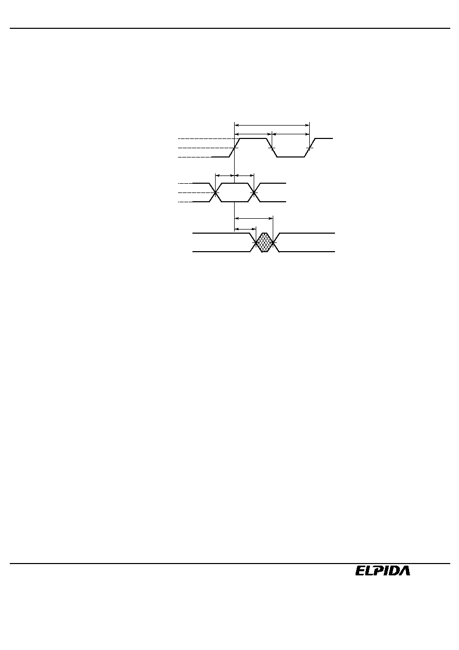
Test Conditions
∑
AC high level input voltage / low level input voltage: 1.6 / 0.2V
∑
Input timing measurement reference level: 0.9V
∑
Transition time (Input rise and fall time): 1ns
∑
Output timing measurement reference level: 0.9V
t
CK
t
CH
t
CL
1.6 V
0.9 V
0.2 V
CLK
1.6 V
0.9 V
0.2 V
Input
t
SETUP
t
HOLD
Output
t
AC
t
OH
EDL1216AASA
Data Sheet E0196E30 (Ver. 3.0)
8
Synchronous Characteristics
Parameter
Symbol
min.
max.
Unit
Note
Clock cycle time
(CL= 2)
tCK2
10
--
ns
(CL= 3)
tCK3
7.5
--
ns
Access time from CLK
(CL= 2)
tAC2
--
6
ns
1
(CL= 3)
tAC3
--
5.4
ns
1
CLK high level width
tCH
2.5
--
ns
CLK low level width
tCL
2.5
--
ns
Data-out hold time
tOH
2.5
--
ns
1
Data-out low-impedance time
tLZ
0
--
ns
Data-out high-impedance time
(CL= 2)
tHZ2
2.5
6
ns
(CL= 3)
tHZ3
2.5
5.4
ns
Data-in setup time
tDS
1.5
--
ns
Data-in hold time
tDH
0.8
--
ns
Address setup time
tAS
1.5
--
ns
Address hold time
tAH
0.8
--
ns
CKE setup time
tCKS
1.5
--
ns
CKE hold time
tCKH
0.8
--
ns
CKE setup time (Power down exit)
tCKSP
1.5
--
ns
Command (/CS, /RAS, /CAS, /WE,
UDQM, LDQM) setup time
tCMS
1.5
--
ns
Command (/CS, /RAS, /CAS, /WE,
UDQM, LDQM) hold time
tCMH
0.8
--
ns
Note: 1. Output load.
Output
Z = 50
30 pF
Output load
Asynchronous Characteristics
Parameter
Symbol
min.
max.
Unit
Notes
ACT to REF/ACT command period (operation) tRC
67.5
ns
ACT to REF/ACT command period (refresh)
tRC1
67.5
ns
ACT to PRE command period
tRAS
45
120000
ns
PRE to ACT command period
tRP
20
ns
Delay time ACT to READ/WRITE command
tRCD
20
ns
ACT (one) to ACT (another) command period
tRRD
15
ns
Data-in to PRE command period
tDPL
15
ns
Data-in to ACT (REF) command period
(Auto precharge)
(CL = 2)
TDAL2
2CLK + 20
ns
(CL = 3)
TDAL3
2CLK + 20
ns
Mode register set cycle time
tRSC
2
CLK
Transition time
tT
0.5
30
ns
Refresh time (4,096 refresh cycles)
tREF
64
ms

EDL1216AASA
Data Sheet E0196E30 (Ver. 3.0)
9
Pin Function
CLK (input pin)
CLK is the master clock input. Other inputs signals are referenced to the CLK rising edge.
CKE (input pins)
CKE determine validity of the next CLK (clock). If CKE is high, the next CLK rising edge is valid; otherwise it is
invalid. If the CLK rising edge is invalid, the internal clock is not issued and the Mobile RAM suspends operation.
When the Mobile RAM is not in burst mode and CKE is negated, the device enters power down mode. During power
down mode, CKE must remain low.
/CS (input pins)
/CS low starts the command input cycle. When /CS is high, commands are ignored but operations continue.
/RAS, /CAS, and /WE (input pins)
/RAS, /CAS and /WE have the same symbols on conventional DRAM but different functions. For details, refer to the
command table.
A0 to A11 (input pins)
Row Address is determined by A0 to A11 at the CLK (clock) rising edge in the active command cycle. It does not
depend on the bit organization.
Column Address is determined by A0 to 8 at the CLK rising edge in the read or write command cycle.
A10 defines the precharge mode. When A10 is high in the precharge command cycle, all banks are precharged;
when A10 is low, only the bank selected by BA0 and BA1 is precharged.
When A10 is high in read or write command cycle, the precharge starts automatically after the burst access.
BA0 and BA1 (input pin)
BA0 and BA1 are bank select signal. (See Bank Select Signal Table)
[Bank Select Signal Table]
BA0
BA1
Bank A
L
L
Bank B
H
L
Bank C
L
H
Bank D
H
H
Remark: H: VIH. L: VIL.
◊
: VIH or VIL
UDQM and LDQM (input pins)
UDQM and LDQM control upper byte and lower byte I/O buffers, respectively. In read mode, DQM controls the
output buffers like a conventional /OE pin. DQM high and DQM low turn the output buffers off and on, respectively.
The DQM latency for the read is two clocks. In write mode, DQM controls the word mask. Input data is written to the
memory cell if DQM is low but not if DQM is high. The DQM latency for the write is zero.
DQ0 to DQ15 (input/output pins)
DQ pins have the same function as I/O pins on a conventional DRAM.
VDD, VSS, VDDQ, VSSQ (Power supply)
VDD and VSS are power supply pins for internal circuits. VDDQ and VSSQ are power supply pins for the output
buffers.

EDL1216AASA
Data Sheet E0196E30 (Ver. 3.0)
10
Command Operation
Extended Mode register set command (/CS, /RAS, /CAS, /WE, BA0 = Low, BA1 = High)
The Mobile RAM has an extended mode register that defines low power functions. In this command, A0 through A11
are the data input pins.
After power on, the extended mode register set command must be executed to fix low power functions.
The extended mode register can be set only when all banks are in idle state.
During tRSC following this command, the Mobile RAM can not accept any other commands.
/WE
/CAS
/RAS
/CS
CKE
CLK
H
Add
A10
BA0
BA1
Extended Mode register set command
Mode register set command (/CS, /RAS, /CAS, /WE, BA0, BA1 = Low)
The Mobile RAM has a mode register that defines how the device operates. In this command, A0 through A11 are
the data input pins. After power on, the mode register set command must be executed to initialize the device. The
mode register can be set only when all banks are in idle state. During tRSC following this command, the Mobile
RAM cannot accept any other commands.
/WE
/CAS
/RAS
/CS
CKE
CLK
H
Add
A10
BA0
BA1
Mode register set command
Activate command (/CS, /RAS = Low, /CAS, /WE = High)
The Mobile RAM has four banks, each with 4,096 rows. This command activates the bank selected by BA0 and BA1
and a row address selected by A0 through A11. This command corresponds to a conventional DRAM's /RAS falling.
/WE
/CAS
/RAS
/CS
CKE
CLK
H
Add
A10
BA0, BA1
Row
Row
Activate command

EDL1216AASA
Data Sheet E0196E30 (Ver. 3.0)
11
Precharge command (/CS, /RAS, /WE = Low, /CAS = High)
This command begins precharge operation of the bank selected by BA0 and BA1. When A10 is High, all banks are
precharged, regardless of BA0 and BA1. When A10 is Low, only the bank selected by BA0 and BA1 is precharged.
After this command, the Mobile RAM can't accept the activate command to the precharging bank during tRP
(precharge to activate command period). This command corresponds to a conventional DRAM's /RAS rising.
/WE
/CAS
/RAS
/CS
CKE
CLK
H
Add
A10
BA0, BA1
(Precharge select)
Precharge command
Write command (/CS, /CAS, /WE = Low, /RAS = High)
This command sets the burst start address given by the column address to begin the burst write operation. The first
write data in burst mode can input with this command with subsequent data on following clocks.
/WE
/CAS
/RAS
/CS
CKE
CLK
H
Add
A10
BA0, BA1
Col.
Write command
Read command (/CS, /CAS = Low, /RAS, /WE = High)
Read data is available after /CAS latency requirements have been met. This command sets the burst start address
given by the column address.
/WE
/CAS
/RAS
/CS
CKE
CLK
H
Add
A10
BA0, BA1
Col.
Read command

EDL1216AASA
Data Sheet E0196E30 (Ver. 3.0)
12
Auto refresh command (/CS, /RAS, /CAS = Low, /WE, CKE = High)
This command is a request to begin the Auto refresh operation. The refresh address is generated internally.
Before executing Auto refresh, all banks must be precharged. After this cycle, all banks will be in the idle
(precharged) state and ready for a row activate command. During tRC1 period (from refresh command to refresh or
activate command), the Mobile RAM cannot accept any other command
Add
A10
BA0, BA1
/WE
/CAS
/RAS
/CS
CKE
CLK
H
Auto refresh command
Self refresh entry command (/CS, /RAS, /CAS, CKE = Low, /WE = High)
After the command execution, self refresh operation continues while CKE remains low. When CKE goes high, the
Mobile RAM exits the self refresh mode. During self refresh mode, refresh interval and refresh operation are
performed internally, so there is no need for external control. Before executing self refresh, all banks must be
precharged.
/WE
/CAS
/RAS
/CS
CKE
CLK
Add
A10
BA0, BA1
Self refresh entry command
Power down entry command (/CS, CKE = Low, /RAS, /CAS, /WE = High)
After the command execution, power down mode continues while CKE remains low. When CKE goes high, the
Mobile RAM exits the power down mode. Before executing power down, all banks must be precharged.
/WE
/CAS
/RAS
/CS
CKE
CLK
Add
A10
BA0, BA1
Power down entry command

EDL1216AASA
Data Sheet E0196E30 (Ver. 3.0)
13
Deep power down entry command( /CS, CKE, /WE = Low, /RAS, /CAS = High)
After the command execution, deep power down mode continues while CKE remains low. When CKE goes high, the
Mobile RAM exits the deep power down mode. Before executing deep power down, all banks must be precharged.
/WE
/CAS
/RAS
/CS
CKE
CLK
Add
A10
BA0, BA1
Deep power down entry command
Burst stop command (/CS = /WE = Low, /RAS, /CAS = High)
This command can stop the current burst operation.
/WE
/CAS
/RAS
/CS
CKE
CLK
Add
A10
BA0, BA1
H
Burst stop command
No operation (/CS = Low, /RAS, /CAS, /WE = High)
This command is not an execution command. No operations begin or terminate by this command.
/WE
/CAS
/RAS
/CS
CKE
CLK
H
Add
A10
BA0, BA1
No operation

EDL1216AASA
Data Sheet E0196E30 (Ver. 3.0)
14
Truth Table
Command Truth Table
CK E
A11,
Function
Symbol
n ≠ 1
n
/CS
/RAS
/CAS
/WE
BA1
BA0
A10
A9 - A0
Device deselect
DESL
H
◊
H
◊
◊
◊
◊
◊
◊
◊
No operation
NOP
H
◊
L
H
H
H
◊
◊
◊
◊
Burst stop
BST
H
H
L
H
H
L
◊
◊
◊
◊
Read
READ
H
◊
L
H
L
H
V
V
L
V
Read with auto precharge
READA
H
◊
L
H
L
H
V
V
H
V
Write
WRIT
H
◊
L
H
L
L
V
V
L
V
Write with auto precharge
WRITA
H
◊
L
H
L
L
V
V
H
V
Bank activate
ACT
H
◊
L
L
H
H
V
V
V
V
Precharge select bank
PRE
H
◊
L
L
H
L
V
V
L
◊
Precharge all banks
PALL
H
◊
L
L
H
L
◊
◊
H
◊
Mode register set
MRS
H
◊
L
L
L
L
L
L
L
V
Extended mode register set
EMRS
H
◊
L
L
L
L
H
L
L
V
Remark: H: VIH. L: VIL.
◊
: VIH or VIL, V = Valid data
DQM Truth Table
CKE
DQM
Function
Symbol
n ≠ 1
n
U
L
Data write / output enable
ENB
H
◊
L
L
Data mask / output disable
MASK
H
◊
H
H
Upper byte write enable / output enable
ENBU
H
◊
L
◊
Lower byte write enable / output enable
ENBL
H
◊
◊
L
Upper byte write inhibit / output disable
MASKU
H
◊
H
◊
Lower byte write inhibit / output disable
MASKL
H
◊
◊
H
Remark: H: VIH. L: VIL.
◊
: VIH or VIL
CKE Truth Table
CK E
Current state
Function
Symbol
n ≠ 1
n
/CS
/RAS
/CAS
/WE
Address
Activating
Clock suspend mode entry
H
L
◊
◊
◊
◊
◊
Any
Clock suspend mode
L
L
◊
◊
◊
◊
◊
Clock suspend
Clock suspend mode exit
L
H
◊
◊
◊
◊
◊
Idle
Auto refresh command
REF
H
H
L
L
L
H
◊
Idle
Self refresh entry
SELF
H
L
L
L
L
H
◊
Idle
Power down entry
PD
H
L
L
H
H
H
◊
H
L
H
◊
◊
◊
◊
Idle
Deep power down entry
DPD
H
L
L
H
H
L
◊
Self refresh
Self refresh exit
L
H
L
H
H
H
◊
L
H
H
◊
◊
◊
◊
Power down
Power down exit
L
H
L
H
H
H
◊
L
H
H
◊
◊
◊
◊
Deep power down
D
d
Deep power down exit
L
H
◊
◊
◊
◊
◊
Remark: H: VIH. L: VIL.
◊
: VIH or VIL
EDL1216AASA
Data Sheet E0196E30 (Ver. 3.0)
15
Function Truth Table
Current state
/CS /RAS /CAS /WE Address
Command
Action
Notes
Idle
H
◊
◊
◊
◊
DESL
Nop
L
H
H
H
◊
NOP
Nop
L
H
H
L
◊
BST
Nop
L
H
L
H
BA, CA, A10
READ/READA ILLEGAL
2
L
H
L
L
BA, CA, A10
WRIT/ WRITA
ILLEGAL
2
L
L
H
H
BA, RA
ACT
Row activating
L
L
H
L
BA, A10
PRE/PALL
Nop
L
L
L
H
◊
REF
Auto refresh
L
L
L
L
OC, BA1= L
MRS
Mode register set
L
L
L
L
OC, BA1= H
EMRS
Extended mode register set
Row active
H
◊
◊
◊
◊
DESL
Nop
L
H
H
H
◊
NOP
Nop
L
H
H
L
◊
BST
Nop
L
H
L
H
BA, CA, A10
READ/READA Begin read
3
L
H
L
L
BA, CA, A10
WRIT/ WRITA
Begin write
3
L
L
H
H
BA, RA
ACT
ILLEGAL
2
L
L
H
L
BA, A10
PRE/PALL
Precharge/Precharge all banks
4
L
L
L
H
◊
REF
ILLEGAL
L
L
L
L
OC, BA
MRS/EMRS
ILLEGAL
Read
H
◊
◊
◊
◊
DESL
Continue burst to end
Row active
L
H
H
H
◊
NOP
Continue burst to end
Row active
L
H
H
L
◊
BST
Burst stop
Row active
L
H
L
H
BA, CA, A10
READ/READA Terminate burst, begin new read
5
L
H
L
L
BA, CA, A10
WRIT/WRITA
Terminate burst, begin write
5, 6
L
L
H
H
BA, RA
ACT
ILLEGAL
2
L
L
H
L
BA, A10
PRE/PALL
Terminate burst
Precharging
L
L
L
H
◊
REF
ILLEGAL
L
L
L
L
OC, BA
MRS/EMRS
ILLEGAL
Write
H
◊
◊
◊
◊
DESL
Continue burst to end
Write recovering
L
H
H
H
◊
NOP
Continue burst to end
Write recovering
L
H
H
L
◊
BST
Burst stop
Row active
L
H
L
H
BA, CA, A10
READ/READA Terminate burst, start read : Determine AP
5, 6
L
H
L
L
BA, CA, A10
WRIT/WRITA
Terminate burst, new write : Determine AP
5
L
L
H
H
BA, RA
ACT
ILLEGAL
2
L
L
H
L
BA, A10
PRE/PALL
Terminate burst
Precharging
7
L
L
L
H
◊
REF
ILLEGAL
L
L
L
L
OC, BA
MRS/EMRS
ILLEGAL
EDL1216AASA
Data Sheet E0196E30 (Ver. 3.0)
16
Current state
/CS /RAS /CAS /WE Address
Command
Action
Notes
Read with auto
H
◊
◊
◊
◊
DESL
Continue burst to end
Precharging
precharge
L
H
H
H
◊
NOP
Continue burst to end
Precharging
L
H
H
L
◊
BST
ILLEGAL
L
H
L
H
BA, CA, A10
READ/READA ILLEGAL
2
L
H
L
L
BA, CA, A10
WRIT/ WRITA
ILLEGAL
2
L
L
H
H
BA, RA
ACT
ILLEGAL
2
L
L
H
L
BA, A10
PRE/PALL
ILLEGAL
2
L
L
L
H
◊
REF
ILLEGAL
L
L
L
L
OC, BA
MRS/EMRS
ILLEGAL
Write with auto
precharge
H
◊
◊
◊
◊
DESL
Continue burst to end
Write recovering
with auto precharge
L
H
H
H
◊
NOP
Continue burst to end
Write recovering
with auto precharge
L
H
H
L
◊
BST
ILLEGAL
L
H
L
H
BA, CA, A10
READ/READA ILLEGAL
2
L
H
L
L
BA, CA, A10
WRIT/ WRITA
ILLEGAL
2
L
L
H
H
BA, RA
ACT
ILLEGAL
2
L
L
H
L
BA, A10
PRE/PALL
ILLEGAL
2
L
L
L
H
◊
REF
ILLEGAL
L
L
L
L
OC, BA
MRS/EMRS
ILLEGAL
Precharging
H
◊
◊
◊
◊
DESL
Nop
Enter idle after tRP
L
H
H
H
◊
NOP
Nop
Enter idle after tRP
L
H
H
L
◊
BST
ILLEGAL
L
H
L
H
BA, CA, A10
READ/READA ILLEGAL
2
L
H
L
L
BA, CA, A10
WRIT/WRITA
ILLEGAL
2
L
L
H
H
BA, RA
ACT
ILLEGAL
2
L
L
H
L
BA, A10
PRE/PALL
Nop
Enter idle after tRP
L
L
L
H
◊
REF
ILLEGAL
L
L
L
L
OC, BA
MRS/EMRS
ILLEGAL
Row activating
H
◊
◊
◊
◊
DESL
Nop
Enter bank active after tRCD
L
H
H
H
◊
NOP
Nop
Enter bank active after tRCD
L
H
H
L
◊
BST
ILLEGAL
L
H
L
H
BA, CA, A10
READ/READA ILLEGAL
2
L
H
L
L
BA, CA, A10
WRIT/WRITA
ILLEGAL
2
L
L
H
H
BA, RA
ACT
ILLEGAL
2, 8
L
L
H
L
BA, A10
PRE/PALL
ILLEGAL
2
L
L
L
H
◊
REF
ILLEGAL
L
L
L
L
OC, BA
MRS/EMRS
ILLEGAL
EDL1216AASA
Data Sheet E0196E30 (Ver. 3.0)
17
Current state
/CS /RAS /CAS /WE Address
Command
Action
Notes
Write recovering H
◊
◊
◊
◊
DESL
Nop
Enter row active after tDPL
L
H
H
H
◊
NOP
Nop
Enter row active after tDPL
L
H
H
L
◊
BST
Nop
Enter row active after tDPL
L
H
L
H
BA, CA, A10
READ/READA Begin read
6
L
H
L
L
BA, CA, A10
WRIT/ WRITA
Begin new write
L
L
H
H
BA, RA
ACT
ILLEGAL
2
L
L
H
L
BA, A10
PRE/PALL
ILLEGAL
2
L
L
L
H
◊
REF
ILLEGAL
L
L
L
L
OC, BA
MRS/EMRS
ILLEGAL
Write recovering H
◊
◊
◊
◊
DESL
Nop
Enter precharge after tDPL
with auto
L
H
H
H
◊
NOP
Nop
Enter precharge after tDPL
precharge
L
H
H
L
◊
BST
Nop
Enter row active after tDPL
L
H
L
H
BA, CA, A10
READ/READA ILLEGAL
L
H
L
L
BA, CA, A10
WRIT/WRITA
ILLEGAL
2, 6
L
L
H
H
BA, RA
ACT
ILLEGAL
2
L
L
H
L
BA, A10
PRE/PALL
ILLEGAL
2
L
L
L
H
◊
REF
ILLEGAL
L
L
L
L
OC, BA
MRS/EMRS
ILLEGAL
Refresh
H
◊
◊
◊
◊
DESL
Nop
Enter idle after tRC1
L
H
H
H
◊
NOP
Nop
Enter idle after tRC1
L
H
H
L
◊
BST
Nop
Enter idle after tRC1
L
H
L
H
BA, CA, A10
READ/READA ILLEGAL
L
H
L
L
BA, CA, A10
WRIT/WRITA
ILLEGAL
L
L
H
H
BA, RA
ACT
ILLEGAL
L
L
H
L
BA, A10
PRE/PALL
ILLEGAL
L
L
L
H
◊
REF
ILLEGAL
L
L
L
L
OC, BA
MRS/EMRS
ILLEGAL
Mode register
H
◊
◊
◊
◊
DESL
Nop
Enter idle after tRSC
accessing
L
H
H
H
◊
NOP
Nop
Enter idle after tRSC
L
H
H
L
◊
BST
Nop
Enter idle after tRSC
L
H
L
H
BA, CA, A10
READ/READA ILLEGAL
L
H
L
L
BA, CA, A10
WRIT/WRITA
ILLEGAL
L
L
H
H
BA, RA
ACT
ILLEGAL
L
L
H
L
BA, A10
PRE/PALL
ILLEGAL
L
L
L
H
◊
REF
ILLEGAL
L
L
L
L
OC, BA
MRS/EMRS
ILLEGAL

EDL1216AASA
Data Sheet E0196E30 (Ver. 3.0)
18
Current state
/CS /RAS /CAS /WE Address
Command
Action
Notes
Extended mode H
◊
◊
◊
◊
DESL
Nop
Enter idle after tRSC
register
L
H
H
H
◊
NOP
Nop
Enter idle after tRSC
accessing
L
H
H
L
◊
BST
Nop
Enter idle after tRSC
L
H
L
H
BA, CA, A10
READ/READA ILLEGAL
L
H
L
L
BA, CA, A10
WRIT/WRITA
ILLEGAL
L
L
H
H
BA, RA
ACT
ILLEGAL
L
L
H
L
BA, A10
PRE/PALL
ILLEGAL
L
L
L
H
◊
REF
ILLEGAL
L
L
L
L
OC, BA0,BA1 MRS/EMRS
ILLEGAL
Remark: H: VIH. L: VIL.
◊
: VIH or VIL, V = Valid data
BA: Bank Address, CA: Column Address, RA: Row Address, OC: Op-Code
Notes: 1. All entries assume that CKE is active (CKE
n-1
=CKE
n
=H).
2. Illegal to bank in specified states; Function may be legal in the bank indicated by Bank Address (BA),
depending on the state of that bank.
3. Illegal if tRCD is not satisfied.
4. Illegal if tRAS is not satisfied.
5. Must satisfy burst interrupt condition.
6. Must satisfy bus contention, bus turn around, and/or write recovery requirements.
7. Must mask preceding data which don't satisfy tDPL.
8. Illegal if tRRD is not satisfied.
EDL1216AASA
Data Sheet E0196E30 (Ver. 3.0)
19
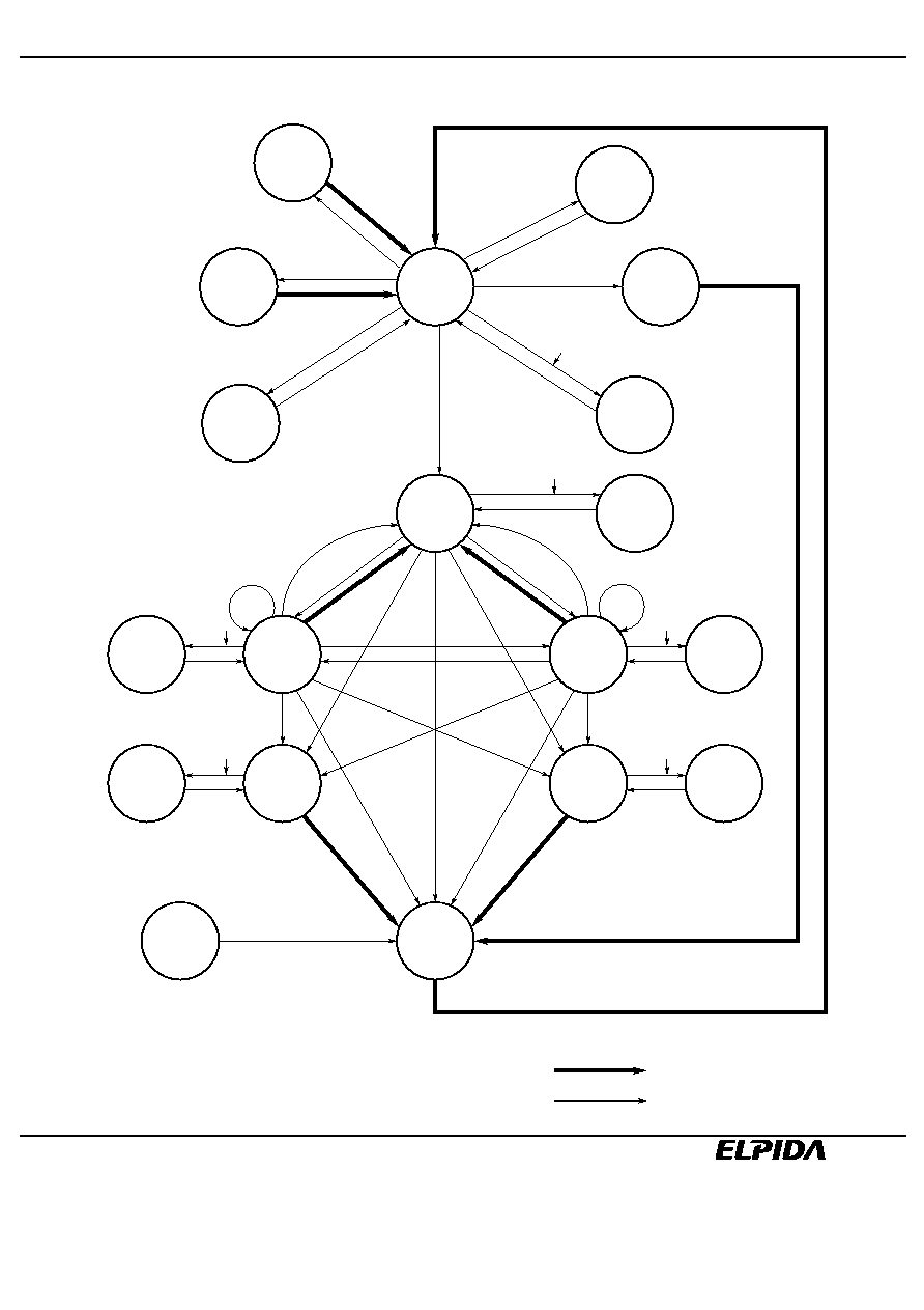
Simplified State Diagram
CKE
CKE
CKE
CKE
CKE
CKE
CKE
CKE
Precharge
Auto precharge
PRE
Read with
Auto precharge
Read
BST
BST
PRE (Precharge termination)
PRE (Precharge termination)
ACT
MRS
REF
CKE
CKE
SELF
SELF exit
IDLE
Mode
Register
Set
Extended
Mode
Register
Set
CBR (Auto)
Refresh
ROW
ACTIVE
Self
Refresh
Power
Down
Active
Power
Down
Precharge
EMRS
READ
READA
READ
SUSPEND
READA
SUSPEND
WRITE
WRITEA
WRITE
SUSPEND
WRITEA
SUSPEND
POWER
ON
Write
Read
Automatic sequence
Manual input
CKE
CKE
Read
Write
Write with
Write
Deep
Power
Down
DPD
DPD exit

EDL1216AASA
Data Sheet E0196E30 (Ver. 3.0)
20
Initialization
The synchronous DRAM is initialized in the power-on sequence according to the following.
(1) To stabilize internal circuits, when power is applied, a 200
µ
s or longer pause must precede any signal toggling.
(2) After the pause, all banks must be precharged using the Precharge command (The Precharge all banks
command is convenient).
(3) Once the precharge is completed and the minimum tRP is satisfied, two or more Auto refresh must be performed.
(4) Both the mode register and the extended mode register must be programmed. After the mode register set cycle
or the extended mode register set cycle, tRSC (2 CLK minimum) pause must be satisfied.
Remarks:
1 The sequence of Auto refresh, mode register programming and extended mode register programming above may
be transposed.
2 CKE and DQM must be held high until the Precharge command is issued to ensure data-bus High-Z.
Programming Mode Registers
The mode register and extended mode register are programmed by the Mode register set command and Extended
mode register command, respectively using address bits A11 through A0, BA0 and BA1 as data inputs. The
registers retain data until they are re-programmed, or the device enters into the deep power down or the device
loses power.
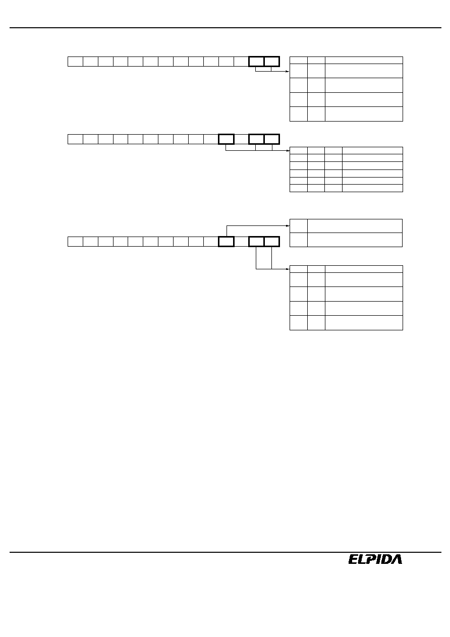
Mode register
The mode register has three fields;
Options
:
A11 through A7
/CAS latency :
A6 through A4
Wrap type
:
A3
Burst length
:
A2 through A0
Following mode register programming, no command can be issued before at least 2 CLK have elapsed.
/CAS Latency
/CAS latency is the most critical of the parameters being set. It tells the device how many clocks must elapse before
the data will be available. The value is determined by the frequency of the clock and the speed grade of the device.
Burst Length
Burst Length is the number of words that will be output or input in a read or write cycle. After a read burst is
completed, the output bus will become High-Z. The burst length is programmable as 1, 2, 4, 8 or full page.
Wrap Type (Burst Sequence)
The wrap type specifies the order in which the burst data will be addressed.
This order is programmable as either
"Sequential" or "Interleave". The method chosen will depend on the type of CPU in the system.
Some microprocessor cache systems are optimized for sequential addressing and others for interleaved addressing.
"Burst Length Sequence" shows the addressing sequence for each burst length using them. Both sequences
support bursts of 1, 2, 4 and 8. Additionally, sequence supports the full page length.

EDL1216AASA
Data Sheet E0196E30 (Ver. 3.0)
21
Extended Mode Register
The extended mode register has four fields;
Options
:
A11 through A7
Drive Strength :
A6 through A5
Temperature Compensated Self Refresh
:
A4 through A3
Partial Array Self Refresh
:
A2 through A0
Following extended mode register programming, no command can be issued before at least 2 CLK have elapsed.
Drive Strength
Driving capability of data output drivers.
Temperature Compensated Self Refresh
Programmable refresh rate for self refresh mode to allow the system to control power as a function of temperature.
Partial Array Self Refresh
Memory array size to be refreshed during self refresh operation is programmable in order to reduce power. Data
outside the defined area will not be retained during self refresh.

EDL1216AASA
Data Sheet E0196E30 (Ver. 3.0)
22
Mode Register Definition
WT = 1
1
2
4
8
R
R
R
R
BL
WT
0
0
0
0
0
Mode Register Set
WT = 0
1
2
4
8
R
R
R
Full page
Bits2-0
000
001
010
011
100
101
110
111
Burst length
Sequential
Interleave
0
1
Wrap type
A0
A1
A2
A3
A4
A5
A7
A6
A8
A9
A10
A11
0
0
Remark R : Reserved
LTMODE
PASR
TCSR
DS
0
0
0
0
0
Extended Mode Register Set
Refresh Array
All banks
Bank A & Bank B (BA1=0)
Bank A (BA0=BA1=0)
R
R
1/2 of Bank A (RA11=0)
1/4 of Bank A (RA11=RA10=0)
R
Bits2-0
000
001
010
011
100
101
110
111
Partial Array
Self Refresh
Max Temperature
70
∞
C
45
∞
C
15
∞
C
85
∞
C
Bits4-3
00
01
10
11
Temprature
Compensated
Self Refresh
Strength
Normal
1/2 strength
1/4 strength
R
Bits6-5
00
01
10
11
Drive Strength
A0
A1
A2
A3
A4
A5
A7
A6
A8
A9
A10
A11
BA1
BA0
BA1
BA0
1
0
/CAS latency
R
R
2
3
R
R
R
R
Bits6-4
000
001
010
011
100
101
110
111
Latency
mode
EDL1216AASA
Data Sheet E0196E30 (Ver. 3.0)
23
Burst Length and Sequence
[Burst of Two]
Starting address
(column address A0, binary)
Sequential addressing sequence
(decimal)
Interleave addressing sequence
(decimal)
0
0, 1
0, 1
1
1, 0
1, 0
[Burst of Four]
Starting address
(column address A1
-
A0, binary)
Sequential addressing sequence
(decimal)
Interleave addressing sequence
(decimal)
00
0, 1, 2, 3
0, 1, 2, 3
01
1, 2, 3, 0
1, 0, 3, 2
10
2, 3, 0, 1
2, 3, 0, 1
11
3, 0, 1, 2
3, 2, 1, 0
[Burst of Eight]
Starting address
(column address A2
-
A0, binary)
Sequential addressing sequence
(decimal)
Interleave addressing sequence
(decimal)
000
0, 1, 2, 3, 4, 5, 6, 7
0, 1, 2, 3, 4, 5, 6, 7
001
1, 2, 3, 4, 5, 6, 7, 0
1, 0, 3, 2, 5, 4, 7, 6
010
2, 3, 4, 5, 6, 7, 0, 1
2, 3, 0, 1, 6, 7, 4, 5
011
3, 4, 5, 6, 7, 0, 1, 2
3, 2, 1, 0, 7, 6, 5, 4
100
4, 5, 6, 7, 0, 1, 2, 3
4, 5, 6, 7, 0, 1, 2, 3
101
5, 6, 7, 0, 1, 2, 3, 4
5, 4, 7, 6, 1, 0, 3, 2
110
6, 7, 0, 1, 2, 3, 4, 5
6, 7, 4, 5, 2, 3, 0, 1
111
7, 0, 1, 2, 3, 4, 5, 6
7, 6, 5, 4, 3, 2, 1, 0
Full page burst is an extension of the above tables of sequential addressing, with the length being 512.
EDL1216AASA
Data Sheet E0196E30 (Ver. 3.0)
24
Address Bits of Bank-Select and Precharge
A11
A10
A9
A8
A7
A6
A4
A5
A3
A2
A1
A0
Row
(Activate command)
A11
A10
A9
A8
A7
A6
A4
A5
A3
A2
A1
A0
(Precharge command)
disables Auto-Precharge
(End of Burst)
0
enables Auto-Precharge
(End of Burst)
1
A11
A10
A9
A8
A7
A6
A4
A5
A3
A2
A1
A0
Col.
(/CAS strobes)
x : Don't care
Select Bank A
"Activate" command
0
Select Bank B
"Activate" command
0
1
1
0
1
0
1
BA1
BA0
BA1
BA0
BA1
BA0
Result
Select Bank C
"Activate" command
Select Bank D
"Activate" command
enables Read/Write
commands for Bank A
0
enables Read/Write
commands for Bank B
0
1
1
0
1
0
1
Result
enables Read/Write
commands for Bank C
enables Read/Write
commands for Bank D
Result
Precharge Bank A
Precharge Bank B
Precharge Bank C
Precharge Bank D
Precharge All Banks
A10
0
0
0
0
1
0
0
1
1
x
0
1
0
1
x
BA1
BA0
BA1
BA0
BA1
BA0
EDL1216AASA
Data Sheet E0196E30 (Ver. 3.0)
25
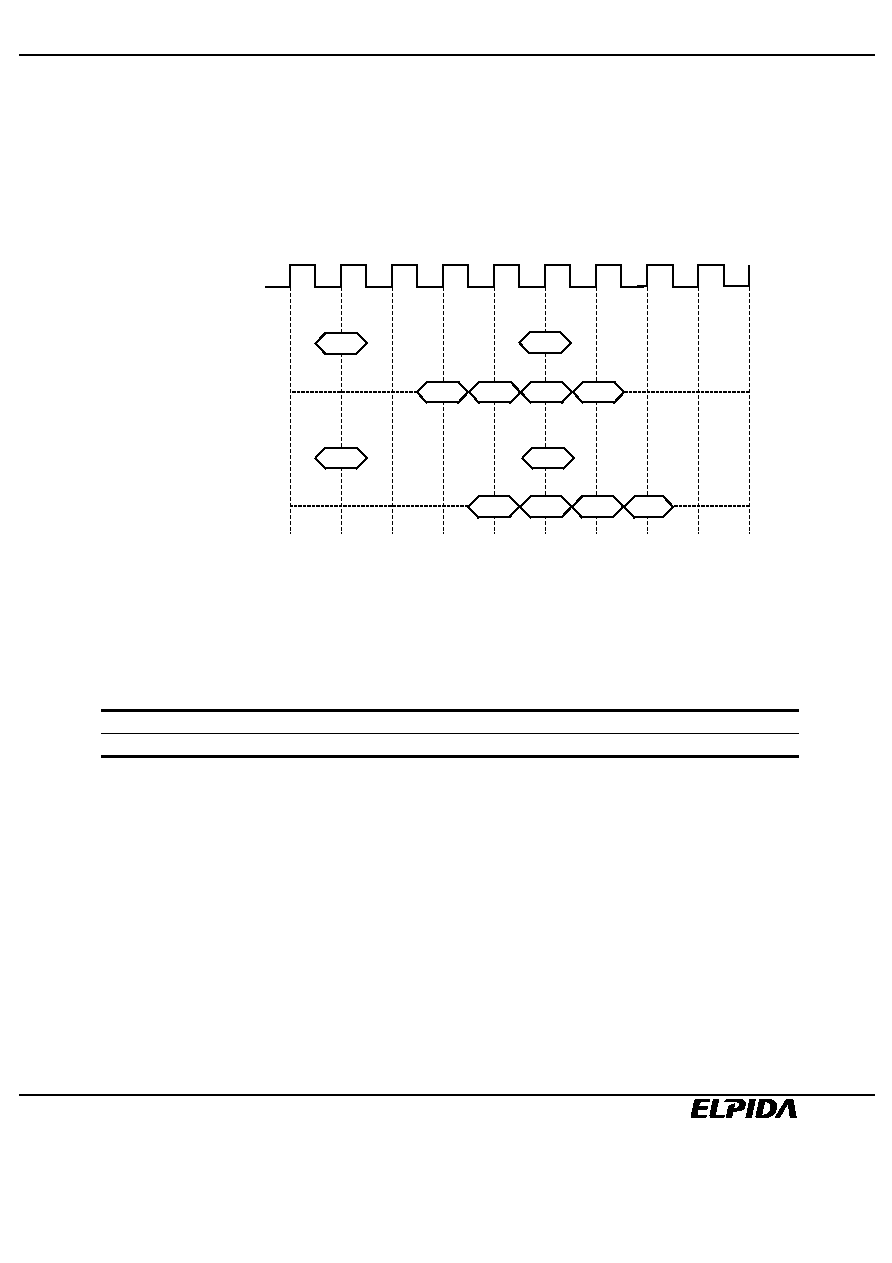
Operation of the Mobile RAM
Precharge
The precharge command can be issued anytime after tRAS
min. is satisfied. Soon after the precharge command is
issued, precharge operation performed and the synchronous DRAM enters the idle state after tRP is satisfied. The
parameter tRP is the time required to perform the precharge. The earliest timing in a read cycle that a precharge
command can be issued without losing any data in the burst is as follows.
T0
T1
T2
T3
T4
T5
T6
T7
Burst length=4
READ
READ
Q1
Q2
Q3
Q4
PRE
Hi-Z
Q1
Q2
Q3
Q4
PRE
Hi-Z
(t
RAS
must be satisfied)
CLK
Command
/CAS latency = 2
DQ
Command
/CAS latency = 3
DQ
T8
Precharge
In order to write all data to the memory cell correctly, the asynchronous parameter tDPL must be satisfied. The tDPL
(min.) specification defines the earliest time that a precharge command can be issued. Minimum number of clocks is
calculated by dividing tDPL (min.) with clock cycle time. In summary, the precharge command can be issued relative
to reference clock that indicates the last data word is valid. In the following table, minus means clocks before the
reference; plus means time after the reference.
/CAS latency
Read
Write
2
-1
+tDPL(min.)
3
-2
+tDPL(min.)

EDL1216AASA
Data Sheet E0196E30 (Ver. 3.0)
26
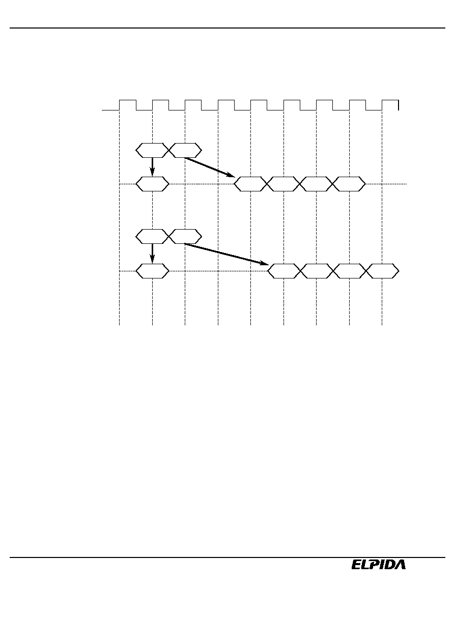
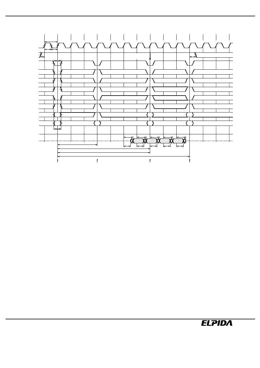
Auto Precharge
During a read or write command cycle, A10 controls whether auto precharge is selected. A10 high in the Read or
Write command (Read with Auto precharge command or Write with Auto precharge command), auto precharge is
selected and begins automatically. The tRAS must be satisfied with a read with auto precharge or a write with auto
precharge operation. In addition, the next activate command to the bank being precharged cannot be executed until
the precharge cycle ends.
In read cycle, once auto precharge has started, an activate command to the bank can be issued after tRP has been
satisfied.
In write cycle, the tDAL must be satisfied to issue the next activate command to the bank being precharged.
The timing that begins the auto precharge cycle depends on whether read or write cycle.
Read with Auto Precharge
During a read cycle, the auto precharge begins one clock earlier (/CAS latency of 2) or two clocks earlier (/CAS
latency of 3) the last data word output.
QB1
QB2
QB3
QB4
Auto precharge starts
READA B
Hi-Z
QB1
QB2
QB3
QB4
Auto precharge starts
READA B
Hi-Z
DQ
Command
DQ
Command
/CAS latency = 2
/CAS latency = 3
CLK
T0
T2
T1
T3
T4
T5
T6
T7
T8
Burst length = 4
(t
RAS
must be satisfied)
T9
Read with Auto Precharge
Remark: READA means Read with Auto precharge
Write with Auto Precharge
During a write cycle, the auto precharge starts at the timing that is equal to the value of the tDPL (min.) after the
last data word input to the device.
DB1
DB2
DB3
DB4
Auto precharge starts
WRITA B
Hi-Z
DQ
Command
CLK
T0
T2
T1
T3
T4
T5
T6
T7
T8
Burst length = 4
(t
RAS
must be satisfied)
t
DPL(MIN.)
Write with Auto Precharge
Remark: WRITA means Write with Auto Precharge

EDL1216AASA
Data Sheet E0196E30 (Ver. 3.0)
27
Read / Write Command Interval
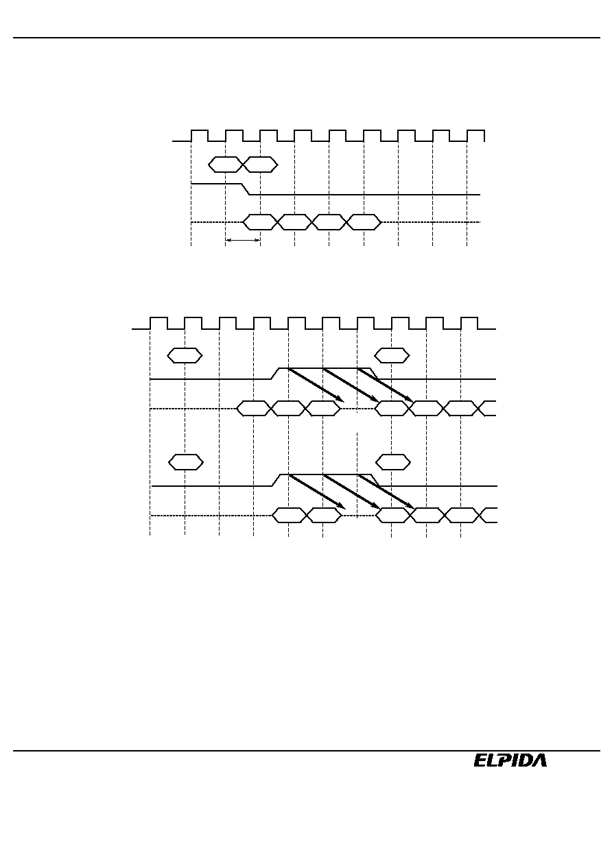
Read to Read Command Interval
During a read cycle, when new Read command is issued, it will be effective after /CAS latency, even if the previous
read operation does not completed. READ will be interrupted by another READ. The interval between the
commands is 1 cycle minimum. Each Read command can be issued in every clock without any restriction.
QB1
QB2
QB3
QB4
Hi-Z
READ A
DQ
Command
CLK
T0
T2
T1
T3
T4
T5
T6
T7
T8
Burst length = 4, /CAS latency = 2
READ B
QA1
1cycle
T9
Read to Read Command Interval
Write to Write Command Interval
During a write cycle, when a new Write command is issued, the previous burst will terminate and the new burst will
begin with a new Write command. WRITE will be interrupted by another WRITE. The interval between the
commands is minimum 1 cycle. Each Write command can be issued in every clock without any restriction.
DB1
DB2
DB3
DB4
Hi-Z
WRITE A
DQ
Command
CLK
T0
T2
T1
T3
T4
T5
T6
T7
T8
Burst length = 4
WRITE B
DA1
1cycle
Write to Write Command Interval
EDL1216AASA
Data Sheet E0196E30 (Ver. 3.0)
28
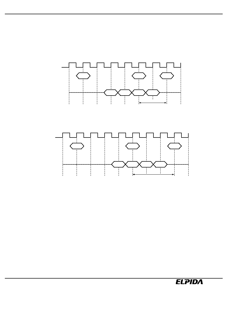
Write to Read Command Interval
Write command and Read command interval is also 1 cycle. Only the write data before Read command will be
written. The data bus must be High-Z at least one cycle prior to the first DOUT.
QB1
QB2
QB3
QB4
WRITE A
Hi-Z
QB1
QB2
QB3
QB4
WRITE A
Hi-Z
DQ
Command
DQ
Command
/CAS latency = 2
/CAS latency = 3
CLK
T0
T2
T1
T3
T4
T5
T6
T7
T8
Burst length = 4
DA1
DA1
READ B
READ B
Write to Read Command Interval
EDL1216AASA
Data Sheet E0196E30 (Ver. 3.0)
29
Read to Write Command Interval
During a read cycle, READ can be interrupted by WRITE. The Read and Write command interval is 1 cycle
minimum. There is a restriction to avoid data conflict. The Data bus must be High-Z using DQM before WRITE.
D1
D2
D3
D4
READ
DQ
Command
CLK
T0
T2
T1
T3
T4
T5
T6
T7
T8
Burst length = 4
WRITE
DQM
Hi-Z
1cycle
Read to Write Command Interval 1
READ can be interrupted by WRITE. DQM must be High at least 3 clocks prior to the Write command.
CLK
T0
T2
T1
T3
T4
T5
T6
T7
T8
Burst length = 8
T9
Q1
Q2
Q3
READ
DQ
Command
D1
D2
D3
WRITE
DQM
Hi-Z is
necessary
Q1
Q2
READ
DQ
Command
D1
D2
D3
WRITE
DQM
Hi-Z is
necessary
/CAS latency = 2
/CAS latency = 3
Read to Write Command Interval 2

EDL1216AASA
Data Sheet E0196E30 (Ver. 3.0)
30
Burst Termination
There are two methods to terminate a burst operation other than using a Read or a Write command. One is the
burst stop command and the other is the precharge command.
Burst Termination in READ Cycle
During a read cycle, when the burst stop command is issued, the burst read data are terminated and the data bus
goes to High-Z after the /CAS latency from the burst stop command.
READ
Command
CLK
T0
T2
T1
T3
T4
T5
T6
T7
Burst length = X
Q1
Q2
Q3
DQ
/CAS latency = 2
Hi-Z
Q1
Q2
Q3
DQ
/CAS latency = 3
Hi-Z
BST
Burst Termination in READ Cycle
Remark: BST: Burst stop command
Burst Termination in WRITE Cycle
During a write cycle, when the burst stop command is issued, the burst write data are terminated and data bus goes
to High-Z at the same clock with the burst stop command.
D2
D3
D4
WRITE
DQ
Command
CLK
T0
T2
T1
T3
T4
T5
T6
T7
Burst length = X
BST
Hi-Z
D1
Burst Termination in WRITE Cycle
Remark: BST: Burst stop command
EDL1216AASA
Data Sheet E0196E30 (Ver. 3.0)
31
Precharge Termination in READ Cycle
During a read cycle, the burst read operation is terminated by a precharge command. When the precharge
command is issued, the burst read operation is terminated and precharge starts. The same bank can be activated
again after tRP from the precharge command. To issue a precharge command, tRAS must be satisfied.
When /CAS latency is 2, the read data will remain valid until one clock after the precharge command.
READ
CLK
T0
T2
T1
T3
T4
T5
T6
T7
Burst length = X, /CAS latency = 2
Q1
DQ
Command
Q2
Q3
Q4
ACT
t
RP
PRE
Hi-Z
(t
RAS
must be satisfied)
Precharge Termination in READ Cycle (CL = 2)
When /CAS latency is 3, the read data will remain valid until two clocks after the precharge command.
READ
CLK
T0
T2
T1
T3
T4
T5
T6
T7
Burst length = X, /CAS latency = 3
DQ
Command
Q1
Q2
Q3
ACT
t
RP
PRE
Hi-Z
T8
Q4
(t
RAS
must be satisfied)
Precharge Termination in READ Cycle (CL = 3)

EDL1216AASA
Data Sheet E0196E30 (Ver. 3.0)
32
Precharge Termination in WRITE Cycle
During a write cycle, the burst write operation is terminated by a precharge command. When the precharge
command is issued, the burst write operation is terminated and precharge starts. The same bank can be activated
again after tRP from the precharge command. To issue a precharge command, tRAS must be satisfied.
The write data written prior to the precharge command will be correctly stored. However, invalid data may be written
at the same clock as the precharge command. To prevent this from happening, DQM must be high at the same
clock as the precharge command. This will mask the invalid data.
WRITE
CLK
T0
T2
T1
T3
T4
T5
T6
T7
Burst length = X, /CAS latency = 3
DQ
Command
D1
D2
D3
ACT
DQM
t
RP
PRE
Hi-Z
D5
T8
D4
(t
RAS
must be satisfied)
Precharge Termination in WRITE Cycle
EDL1216AASA
Data Sheet E0196E30 (Ver. 3.0)
33
Timing Waveforms
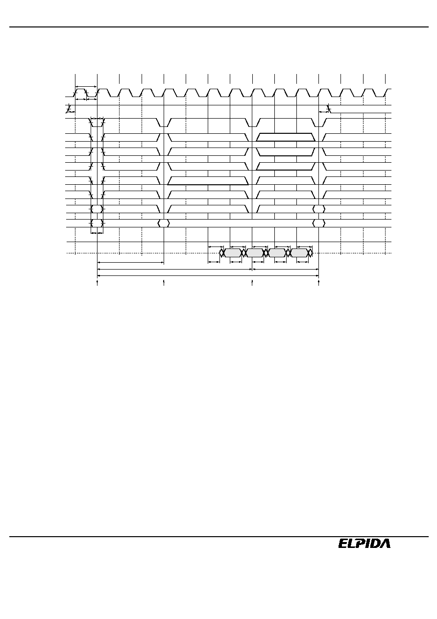
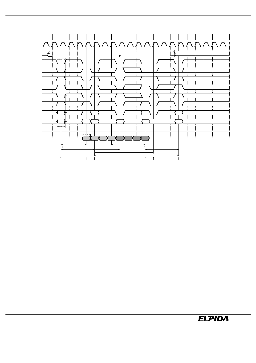
AC Parameters for Read Timing with Manual Precharge
;;;
;;
;;;;
;;;
;;;
;;;;
;;;
;;;
;;;;
;;;;
;;;
;;;
;;;
;;;
;;;;
;;;;
;;;
;;;;
;;;
;;;;
;;;
;;;
;;;
;;;
;;;
;;;
;;;
;;;
;;;
;;;
;;;
;;;
;;;;;;
;;;
t
OH
;
;
;
;
;
;
t
LZ
t
AC
t
OH
t
AC
t
AC
t
OH
;
;
;;
;;
t
OH
t
AC
t
HZ
t
RAS
t
RC
;;;;
;;;
;;;;
BA0
t
CKH
t
RP
;;;
;;;
T0
T1
T2
T3
T4
T5
T6
T7
T8
T9
T10
T11
T12
T13
;;
;
;
;;
;;
;;
;;
;;
;
;
CLK
CKE
/CS
/RAS
/CAS
/WE
BA1
A10
ADD
DQM
DQ
t
RCD
t
CKS
t
CH
t
CL
t
CK
t
CMS
t
CMH
t
AS
t
AH
L
Hi-Z
Activate
Command
for Bank A
Precharge
Command
for Bank A
Read
Command
for Bank A
Activate
Command
for Bank A
[Burst Length = 4, /CAS Latency = 3]
EDL1216AASA
Data Sheet E0196E30 (Ver. 3.0)
34
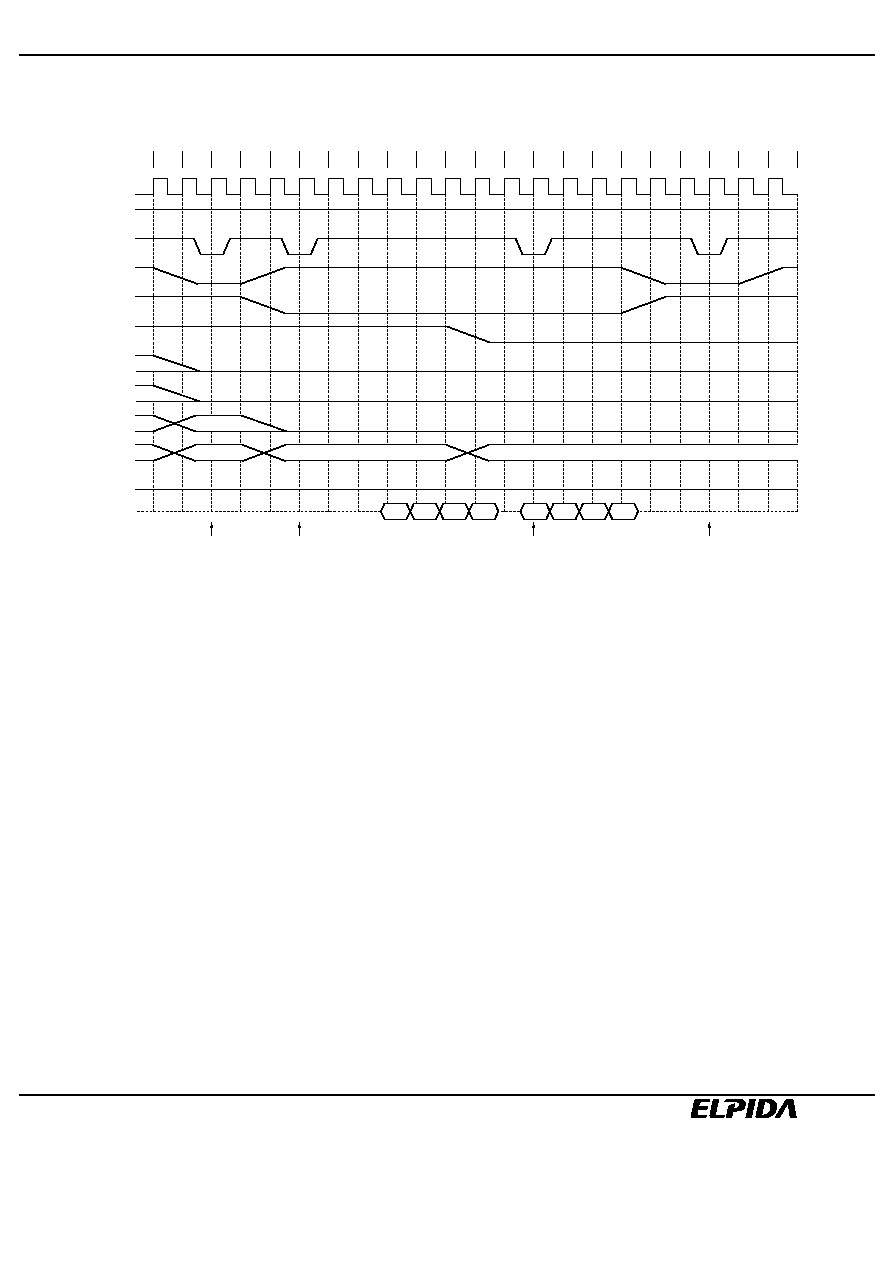
AC Parameters for Read Timing with Auto Precharge
t
CKS
;;
;;
;;
;;
;;;
;;;
;;
;;
;;;
;;;
;;;
;;;
;;
;;
;;;
;;;
;;;
;;;
;;;
;;;;;
;;;;;
;;;;;;
;;;
;;;
;;;;
;;;;
;;;
;;;
;;;
;;;
;;;
;;;;
;;;
t
OH
;
;
;
t
LZ
t
AC
t
OH
t
AC
t
AC
t
OH
;
;
;
;
t
OH
t
AC
t
HZ
t
RAS
t
RRD
t
RC
;;;
;;;
;;;
;;;
;;;
;;;
BA0
t
CKH
;;;;
T0
T1
T2
T3
T4
T5
T6
T7
T8
T9
T10
T11
T12
T13
;;
;;
;
;;
;;
;;
;;
CLK
CKE
/CS
/RAS
/CAS
/WE
BA1
A10
ADD
DQM
DQ
t
RCD
t
CH
t
CL
t
CK
t
CMS
t
CMH
t
AS
t
AH
L
Hi-Z
;;;
;;;
;;;
Auto Precharge
Start for Bank C
Activate
Command
for Bank C
Activate
Command
for Bank D
Read with
Auto Precharge
Command
for Bank C
Activate
Command
for Bank C
[Burst Length = 4, /CAS Latency = 3]
EDL1216AASA
Data Sheet E0196E30 (Ver. 3.0)
35
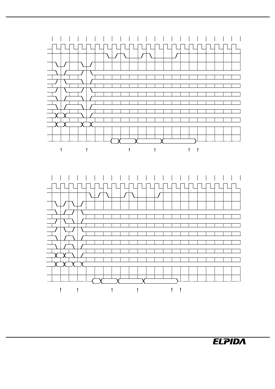
AC Parameters for Write Timing
;;
;;
;;
;;
;;
;;
;;
;;
;;
;;;;
;;;;
;;;;;;
;;
;;
;;;;
;;;
;;
;;
;;
;;
;;
;;
;;
;;
;;;;
;;;
;;;
;;
;;
;;
;;
;;
;;
;;;;
;;;;
;;
;;
;;
;;;;
;;;;
;;
;;
;;
;;;;
;;;;
;;;
T0
T1
T2
T3
T4
T5
T6
T7
T8
T9
T10
T11
T12
T13
T14
T15
T16
T17
T18
T19
T20
T21
;;;;
;;
;;
CLK
CKE
BA0
A10
ADD
DQM
DQ
Hi-Z
t
AS
t
AH
t
DS
t
DH
t
RCD
t
DAL
t
RC
t
RRD
t
RCD
t
RAS
t
RC
t
DPL
t
RP
t
CKH
;;
;;
t
CMS
t
CMH
t
CKS
/CS
/RAS
/CAS
/WE
;;
;;
;;
;;
;;;
;;;
;;
;;
BA1
;;
Auto Precharge
Start for Bank C
L
;;
;;
Activate
Command
for Bank C
Activate
Command
for Bank B
Write
Command
for Bank B
Activate
Command
for Bank B
Write with
Auto Precharge
Command
for Bank C
Precharge
Command
for Bank B
Activate
Command
for Bank C
[Burst Length = 4]

EDL1216AASA
Data Sheet E0196E30 (Ver. 3.0)
36
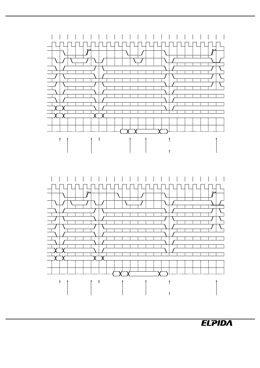
Mode Register Set
CLK
CKE
/CS
/RAS
/CAS
/WE
BA0
A10
ADD
DQM
DQ
;;
;;;;;;;;;
;;
;;
;;
;;
;;;;;;;;;
;;;;;;;;;
;;
;;
;;
;;
;;
;;
;;
;;;;;;;;;
;;;
;;
;;
;;
;
;
;;;;;;;;;
;;;
;;;
;;
;;
;;;;;;;;
;;;;;;;;
;
;
;;;;;;;;
;;;;;;;;
;;;;;;;;
;
;;;
;;;;;;;;;;;;
BA1
T0
T1
T2
T3
T4
T5
T6
T7
T8
T9
T10
T11
T12
T13
T14
T15
T16
T17
T18
T19
T20
T21
Hi-Z
ADDRESS KEY
t
RP
Precharge
All Banks
Command
Mode
Register Set
Command
Activate
Command
is valid
H
t
RSC
2 CLK (MIN.)

EDL1216AASA
Data Sheet E0196E30 (Ver. 3.0)
37
Extended Mode Register Set
CLK
CKE
/CS
/RAS
/CAS
/WE
BA0
A10
ADD
DQM
DQ
;;
;;;;;;;;;
;;
;;
;;
;;
;;;;;;;;;
;;;;;;;;;
;;
;;
;;
;;
;;
;;
;;
;;;;;;;;;
;;;
;;
;;
;;
;
;
;;;;;;;;;
;;;
;;;
;;
;;
;;;;;;;;
;;;;;;;;
;
;
;;;;;;;;
;;;;;;;;
;;;;;;;;
;
;;;
;;;;;;;;;;;;
BA1
T0
T1
T2
T3
T4
T5
T6
T7
T8
T9
T10
T11
T12
T13
T14
T15
T16
T17
T18
T19
T20
T21
Hi-Z
ADDRESS KEY
t
RP
Precharge
All Banks
Command
Extended
Mode
Register Set
Command
Activate
Command
is valid
H
t
RSC
2 CLK (MIN.)
Power On Sequence
CLK
CKE
/CS
/RAS
/CAS
/WE
BA1
A10
ADD
DQM
DQ
;;
;;
;
;
;
;
;
;
;
;
;
;
;
;;
;;
;
;
;;;
;;;
;;;
;;
;;;;;;;;
;;;;;;;;
;;
;;
;;
;;;;;;;;
;;
;;
;;;;;;;;
;;;
Hi-Z
t
RSC
t
RSC
ADDRESS KEY ADDRESS KEY
t
RP
;
;
;
;
;
;
;
;
;;;
;;;
;;;
;;;
;;;
;;;;
;;;;
;;;;
;;;;
;;;;
;;
;;
;;
;;
;;
;;
;;
;;
;;
;;
High level is necessary
2 refresh cycles are necessary
t
RC1
t
RC1
Precharge
All Banks
Command
is necessary
Mode
Register Set
Command
is necessary
Extended
Mode
Register Set
Command
is necessary
CBR (Auto)
Refresh
Command
is necessary
Activate
Command
CBR (Auto)
Refresh
Command
is necessary
BA0
;;;
;;;;;;;;
High level is necessary
Clock cycle is necessary
EDL1216AASA
Data Sheet E0196E30 (Ver. 3.0)
38
/CS Function
Only /CS signal needs to be issued at minimum rate
CLK
CKE
/CS
/RAS
/CAS
/WE
BA1
A10
ADD
DQM
DQ
T0
T1
T2
T3
T4
T5
T6
T7
T8
T9
T10
T11
T12
T13
T14
T15
T16
T17
T18
T19
T20
T21
H
L
Hi-Z
L
BA0
L
RAa
QAa1
QAa2
QAa3
QAa4
DAb1
DAb2
DAb3
DAb4
Activate
Command
for Bank A
Read
Command
for Bank A
Write
Command
for Bank A
Precharge
Command
for Bank A
RAa
CAa
CAb
[Burst Length = 4, /CAS Latency = 3]
EDL1216AASA
Data Sheet E0196E30 (Ver. 3.0)
39
Clock Suspension during Burst Read
CLK
CKE
/CS
/RAS
/CAS
/WE
BA1
A10
ADD
DQM
DQ
;;
T0
T1
T2
T3
T4
T5
T6
T7
T8
T9
T10
T11
T12
T13
T14
T15
T16
T17
T18
T19
T20
T21
;;
;;;
;;;;;;;;;;
;;;;;;;;;;
;;;;;;;;;;
;;
;;
;;
;;;;;;;;;;
QAa1
QAa2
QAa3
QAa4
CAa
;;
;;;;;;;;;;
;;
;;
;
;
;;
;;
;;;;;;;;;;
;;
;
;;
;;
;
;;;;;;;;;;
;;;;;;;;;;
;;
;;
;;
;;;
;;
BA0
;;
;;
;;;;;;;;;;
;;;;;;;;;;
;;
;;
;;
;;
L
Hi-Z
RAa
RAa
Activate
Command
for Bank A
Read
Command
for Bank A
1-CLOCK
SUSPENDED
2-CLOCK
SUSPENDED
3-CLOCK
SUSPENDED
Hi-Z (turn off)
at the end of burst
[Burst Length = 4, /CAS Latency = 3]
CLK
CKE
/CS
/RAS
/CAS
/WE
BA1
A10
ADD
DQM
DQ
;;
T0
T1
T2
T3
T4
T5
T6
T7
T8
T9
T10
T11
T12
T13
T14
T15
T16
T17
T18
T19
T20
T21
;
;;;
;;;;;;;;;;
;;;;;;;;;;
;;;;;;;;;;
;
;
;
;
;;;;;;;;;;
;;;;;;;;;;
QAa1
QAa2
QAa3
QAa4
CAa
;;
;;;;;;;;;;
;
;
;;
;;
;;;;;;;;;;
;
;
;;
;;
;
;;;;;;;;;;
;;;;;;;;;;
;
;;
;;
;
;
;
BA0
;;;;;;;;;;;;
;;
;
;
L
Hi-Z
RAa
RAa
Activate
Command
for Bank A
Read
Command
for Bank A
1-CLOCK
SUSPENDED
2-CLOCK
SUSPENDED
3-CLOCK
SUSPENDED
Hi-Z (turn off)
at the end of burst
;;;
[Burst Length = 4, /CAS Latency = 2]

EDL1216AASA
Data Sheet E0196E30 (Ver. 3.0)
40
Clock Suspension during Burst Write
CLK
CKE
/CS
/RAS
/CAS
/WE
BA1
A10
ADD
DQM
DQ
;;
T0
T1
T2
T3
T4
T5
T6
T7
T8
T9
T10
T11
T12
T13
T14
T15
T16
T17
T18
T19
T20
T21
;;
;;;
;;;;;;;;;;
;;;;;;;;;;
;;;;;;;;;;
;;
;;
;;;
;;;;;;;;;;
CAa
;;
;;;;;;;;;;
;
;
;;
;;
;;;;;;;;;;
;
;;
;;
;
;;;
;;
BA0
;;
;;
;;;;;;;;;;
;;;;;;;;;;
;;
;;
;;
;;
L
Hi-Z
RAa
RAa
;;
;;
;;
;;
;;;;;;;;;;
;;;;;;;;;;
;
;
;;;
;;;
DAa1
DAa2
DAa3
DAa4
Activate
Command
for Bank A
1-CLOCK
SUSPENDED
2-CLOCK
SUSPENDED
3-CLOCK
SUSPENDED
Write
Command
for Bank A
EDL1216AASA
Data Sheet E0196E30 (Ver. 3.0)
41
Power Down Mode and Clock Mask
CLK
CKE
/CS
/RAS
/CAS
/WE
BA1
A10
ADD
DQM
DQ
;;
;;
T0
T1
T2
T3
T4
T5
T6
T7
T8
T9
T10
T11
T12
T13
T14
T15
T16
T17
T18
T19
T20
T21
;
;
;;;;
;;;;;;;;
;;;
;;;
QAa3
CAa
;;
;;;
;;;
;;
;
;;
;;;
;;
;
;;
;
;;
;;;
;;;
;;;
;
;
L
Hi-Z
RAa
;;
;;;
;;;;
;;;;
;;;;;
;;;;;
;;;;
;;;;;
;;;;
;;;;;
;;;;;
;;;;;
;;;;;
;;;;
;;;;
BA0
;;
;;
;;;;
;;;
;;;
;;;;;
;;;;;
;;;;
;;;;
;;;;
t
CKSP
t
CKSP
QAa1 QAa2
VALID
Activate
Command
for Bank A
Power Down
Mode Entry
ACTIVE STANDBY
Power Down
Mode Exit
Read
Command
for Bank A
Clock Mask
Start
Clock Mask
End
Power Down
Mode Entry
Precharge
Command
for Bank A
PRECHARGE STANDBY
Power Down
Mode Exit
QAa4
RAa
;
[Burst Length = 4, /CAS Latency = 3]
CLK
CKE
/CS
/RAS
/CAS
/WE
BA1
A10
ADD
DQM
DQ
;;
T0
T1
T2
T3
T4
T5
T6
T7
T8
T9
T10
T11
T12
T13
T14
T15
T16
T17
T18
T19
T20
T21
;;
;;;;
;;;;;;;;
;;;;;;;;
;;;
;;;
;;;
;;;
QAa3
CAa
;;
;;
;;;
;
;;
;;
;;;
;
;;
;;
;;
;;
;
;;;
;;;
;;;
;;
;;
;;
;;
L
Hi-Z
RAa
;;
;;
;;;
;;;
;;;;
;;;;;
;;;;
;;;;;
;;;;
;;;;
;;;;;
;;;;;
;;;;;
;;;;;
;;;;;
;;;;
BA0
;;
;;;;
;;;
;;;;;;;;;
;;;;
;;;;
t
CKSP
t
CKSP
QAa1 QAa2
VALID
Activate
Command
for Bank A
Power Down
Mode Entry
ACTIVE STANDBY
Power Down
Mode Exit
Read
Command
for Bank A
Clock Mask
Start
Clock Mask
End
Power Down
Mode Entry
Precharge
Command
for Bank A
PRECHARGE STANDBY
Power Down
Mode Exit
QAa4
RAa
;;
;;
[Burst Length = 4, /CAS Latency = 2]
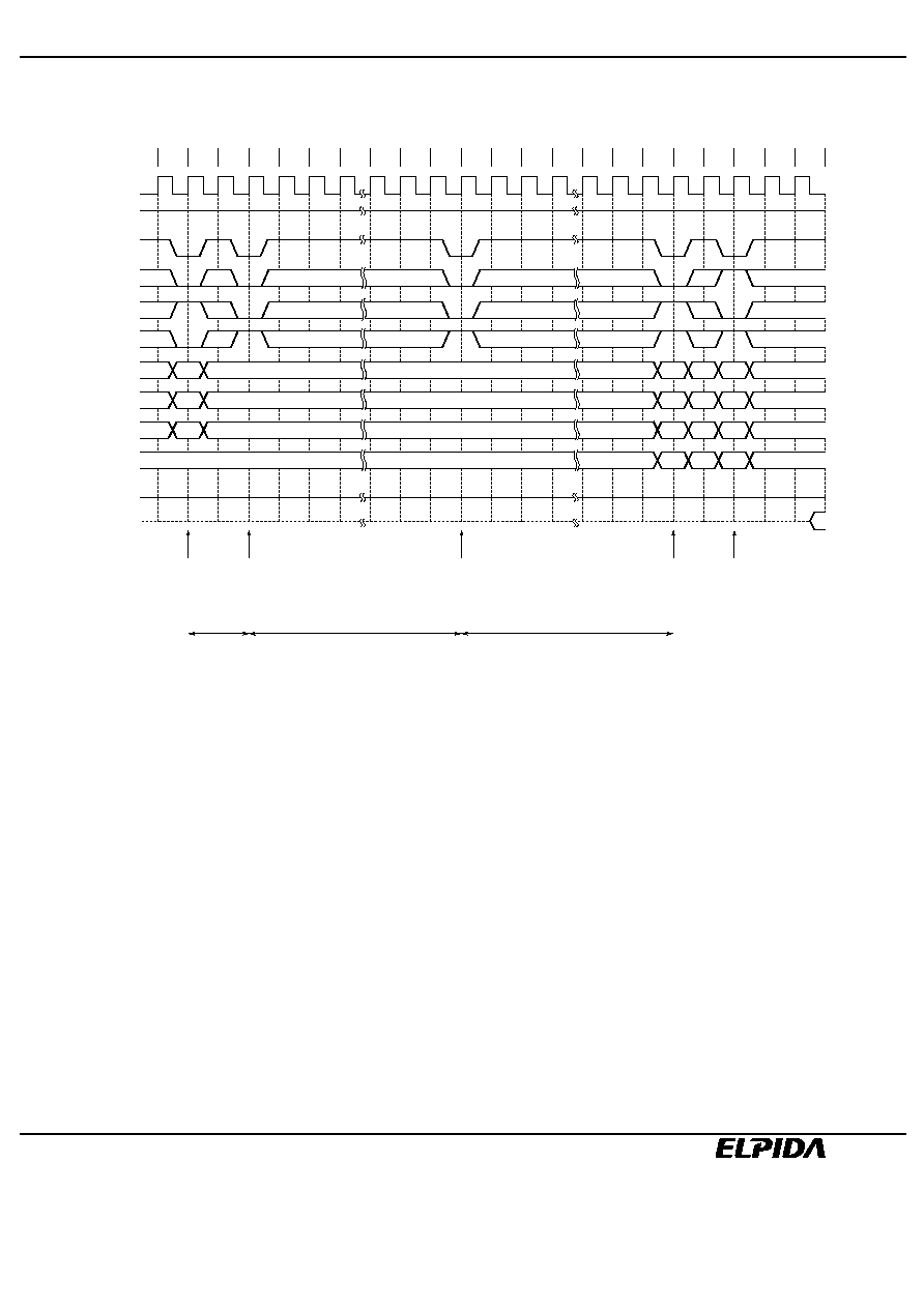
EDL1216AASA
Data Sheet E0196E30 (Ver. 3.0)
42
Auto Refresh
CLK
CKE
/CS
/RAS
/CAS
/WE
BA1
A10
ADD
DQM
DQ
T0
T1
T2
T3
T4
T5
T6
Tn
Tn
+
1 Tn
+
2
Tn
+
3 Tn
+
4
Tn
+
5 Tn
+
6
Tm
Tm
+
1 Tm
+
2 Tm
+
3 Tm
+
4 Tm
+
5 Tm
+
6 Tm
+
7
;
;;
;
;;;;;;;;;
;;;;;;;;;
;;
;;
;
;
;;;;;;;;
;;
BA0
;;;
;;;
;;
;;
;;;;;;;;
;;;;;;;;
;
;
;
;;;
;;;;;
;
;;;;
;;
;;;
;
;
;
;;
;
;;;;
;;
;;
;
;
;;;;
;
;;
;
;
;;
;
;;;;
;;;;
;
;
;;
;;;;
;;;;
;
;;
;;;
;
L
Hi-Z
t
RP
H
t
RC1
t
RC1
Q1
Precharge
Command
(if necessary)
CBR (Auto) Refresh
CBR (Auto) Refresh
Activate
Command
Read
Command
;;
;;;
;;;
;;;;;;;;
;;

EDL1216AASA
Data Sheet E0196E30 (Ver. 3.0)
43
Self Refresh (Entry and Exit)
CLK
CKE
/CS
/RAS
/CAS
/WE
BA1
A10
ADD
DQM
DQ
;
;
;;
;;
;;
;;
;;
;;
;;
;;
;;;
;;;
;;;
;;;
;;;;;;;;;;;
T0
T1
T2
T3
T4
Tn
Tn
+
1 Tn
+
2
Tm
Tm
+
1
Tk
Tk
+
1
Tk
+
2 Tk
+
3
Tk
+
4
t
RP
;;;;;
;;;;;
;;;;;
;;;;
;;;;
;;;;
;;;;
;;
;;
;;
;;
;;
;;
;;
;;
;;
t
RC1
t
RC1
;;;;;
;;;
;;;
;;;;;;;;;;;
BA0
;;
;;
;;;;;;;;;
Precharge
Command
(if necessary)
Self Refresh
Entry
Self Refresh
Exit
Next Clock
Enable
Self Refresh
Entry
(or Activate Command)
Activate
Command
Self Refresh
Exit
Next Clock
Enable
L
Hi-Z
;;
;;
;;;;;;;;;
;;;;;;;;;

EDL1216AASA
Data Sheet E0196E30 (Ver. 3.0)
44
Deep Power Down Entry
CLK
CKE
/CS
/RAS
/CAS
/WE
BA0
A10
ADD
DQM
DQ
;;
;;
;;;;;;;;;;;;
;;;;;;;;;;;
;;;;;;;;;;;
;;;;;;;;;;
;;;;;;;;;;
;;
;;
;;
;;
;;
;;
;;
;;;;;;;;;;;;
BA1
;;;;;;;;;;;;
;;;;;;;;;;;;
;;;;;;;;;;;;
T0
T1
T2
T3
T4
T5
T6
T7
T8
T9
T10
T11
T12
T13
T14
T15
T16
T17
T18
T19
T20
T21
Hi-Z
t
RP
Precharge
All Banks
Command
Deep
Power Down
Entry
;;;;;;;;;;
;;;;;;;;;;
L
Deep Power Down Exit
CLK
CKE
/CS
/RAS
/CAS
/WE
BA1
A10
ADD
DQM
DQ
;;
;;
;
;
;
;
;
;
;
;
;
;
;
;;
;;
;
;
;;;
;;;
;;;
;;
;;;;;;;;
;;;;;;;;
;;
;;
;;
;;;;;;;;
;;
;;
;;;;;;;;
;;;
Hi-Z
t
RSC
t
RSC
ADDRESS KEY ADDRESS KEY
t
RP
200
µ
s
;
;
;
;
;
;
;
;
;;;
;;;
;;;
;;;
;;;
;;;;
;;;;
;;;;
;;;;
;;;;
;;
;;
;;
;;
;;
;;
;;
;;
;;
;;
High level is necessary
2 refresh cycles are necessary
t
RC1
t
RC1
Precharge
All Banks
Command
is necessary
Deep
Power Down
Exit
Command
Mode
Register Set
Command
is necessary
Extended
Mode
Register Set
Command
is necessary
CBR (Auto)
Refresh
Command
is necessary
Activate
Command
CBR (Auto)
Refresh
Command
is necessary
BA0
;;;
;;;;;;;;
High level is necessary
Clock cycle is necessary
;

EDL1216AASA
Data Sheet E0196E30 (Ver. 3.0)
45
Random Column Read
CLK
CKE
/CS
/RAS
/CAS
/WE
BA1
A10
ADD
DQM
DQ
Precharge
Command
for Bank A
Activate
Command
for Bank A
Read
Command
for Bank A
Read
Command
for Bank A
Read
Command
for Bank A
Activate
Command
for Bank A
Read
Command
for Bank A
T0
T1
T2
T3
T4
T5
T6
T7
T8
T9
T10
T11
T12
T13
T14
T15
T16
T17
T18
T19
T20
T21
;
;
;;;;;
;;;;;;;;;;;;
;;
;;
;;
;;
;;
;;;;;
;;
;;;
;;;
;;
;;
;
;
;;
;;
;;
;;
;;
;;
;;
;;
QAa1
QAa2
;;;;;;;;;;;;
;;
;;
;;
;;
;;
;
;
;
;
;
;
;
;
;;
;;
;;
;;
;;;
;;;
;;;
;;;
;;
;;;
;;;
QAa3
QAa4
QAb1
QAb2
QAc1
QAc2
QAc3
QAc4
;;;;
;;
;;
H
RAa
RAa
CAa
CAc
CAa
RAa
CAb
;;
;;
;;;;
;;
BA0
;;
;;;;;
;;;
;
;;
;;;;
;;
;;
;;
;;
;;
;;
;;
;;
;;
;;
;;
;;
;;
;;
;;
;;;
;;
;;
;
;;
;;
RAa
;;
L
Hi-Z
[Burst Length = 4, /CAS Latency = 3]
CLK
CKE
/CS
/RAS
/CAS
/WE
BA1
A10
ADD
DQM
DQ
;;
;;
T0
T1
T2
T3
T4
T5
T6
T7
T8
T9
T10
T11
T12
T13
T14
T15
T16
T17
T18
T19
T20
T21
;
;
;;;;;
;;;;;;;;;;;;
;
;;
;;
;
;;
;;
;
;;;
;;;
;;
;;
;
;
;
;
;
;
;
;
;;;
;;;
;;;
;;;
QAa1
QAa2
;;;;;;;;;;;;;
;;;
;;;
;;;
;;
;;
;;
;;
;;
;;
;;
;;;;
;;;;
;;;;
;;;;
;;;;
;;;
;;;
;;;
;;;
;;;
;;
;;
;;
;;
;
;;
;;
QAa3
QAa4
QAb1
QAb2
QAc1
QAc2
QAc3
QAc4
QAd1
QAd2
QAd3
;;;;
;
;
H
RAd
RAa
CAd
CAc
CAa
RAd
CAb
;;
;;
;;
;
;
;
;
;
;
BA0
;;
;;;;
;;;
;;
;;;;
;;;
;;;;
;;
;;
;;
;;
;;
;;
;;
;;
;;
;;
;;
;;
;;
;
;
;
;
;;
;
;
;
;
;
RAa
Precharge
Command
for Bank A
Activate
Command
for Bank A
Read
Command
for Bank A
Read
Command
for Bank A
Read
Command
for Bank A
Activate
Command
for Bank A
Read
Command
for Bank A
L
Hi-Z
[Burst Length = 4, /CAS Latency = 2]

EDL1216AASA
Data Sheet E0196E30 (Ver. 3.0)
46
Random Column Write
CLK
CKE
/CS
/RAS
/CAS
/WE
BA1
A10
ADD
DQM
DQ
;;
T0
T1
T2
T3
T4
T5
T6
T7
T8
T9
T10
T11
T12
T13
T14
T15
T16
T17
T18
T19
T20
T21
;
;;;;;
;;;;;;;;;;;;
;;;;;;;;;;;;
;;
;;
;;
;;
;;
;
;;
;;
;;;
;;
;
L
Hi-Z
;;
;;
;;
;;
DDa1
DDa2
;;;;;;;;;;;;;
;;
;;
;;
;;
;
;
;
;
;;
;;
;;
;;
;;;
;;;
;;
;;;
DDa3
DDa4
DDb1
DDb2
DDc1
DDc2
DDc3
DDc4
;;;;
;;
;;
H
RDd
RDa
CDd
CDc
CDa
RDd
CDb
;;
;;;;
;;
BA0
;;
;;
;;;;;
;;
;;
;
;
;;
;;
;;
;;
;;;;
;;
;;
;;
;;
;;
;;
;;
;;
;;
;;
;;
;;
;;
;;
;
;;
;;
;;
;
;;
;;
RDa
DDd1
;;
;;
;;
;;
;;
;;
;;
;;
;;
Activate
Command
for Bank D
Write
Command
for Bank D
Write
Command
for Bank D
Write
Command
for Bank D
Precharge
Command
for Bank D
Activate
Command
for Bank D
Write
Command
for Bank D
DDd2
[Burst Length = 4]

EDL1216AASA
Data Sheet E0196E30 (Ver. 3.0)
47
Random Row Read
CLK
CKE
/CS
/RAS
/CAS
/WE
BA0
A10
ADD
DQM
DQ
;;
T0
T1
T2
T3
T4
T5
T6
T7
T8
T9
T10
T11
T12
T13
T14
T15
T16
T17
T18
T19
T20
T21
;;
;;
;;;;;;;;;;;;;
;;
;;
;;
;;
;;
;
;;
;;;
;;;
;;;
;;;
;;
;;
L
Hi-Z
;;
QBa1
QBa2
;;;;;;;;;;;;
;;;
;;
;;
;;
QBa3
QBa4
QBa5
QBa6
QBa7
QBa8
QAa1
QAa2
QAa3
QAa4
QAa5
H
RBb
RBa
CBb
CAa
CBa
RBb
RAa
;;
;;
;;
;;
;;
;;
;;
;;
;;
;;
;
;
;
RBa
;
;;
;;;;;;
;
;;
;;
;;;
;;;
;;
;;
;;
;
;;
;;
;;
RAa
;;
;;
;;;
;;;
QAa6
QAa7
;;
;;
;;
;;
;;
;
;
;;
;;
;;
;;
;;
;;
;
;
;;
;
;
;;;
;;
;
;;
;;
;;
;;;
;
;
BA1
Activate
Command
for Bank B
Read
Command
for Bank B
Activate
Command
for Bank A
Read
Command
for Bank A
Precharge
Command
for Bank B
Activate
Command
for Bank B
Read
Command
for Bank B
Precharge
Command
for Bank A
;
;
;;
[Burst Length = 8, /CAS Latency = 3]
CLK
CKE
/CS
/RAS
/CAS
/WE
BA1
A10
ADD
DQM
DQ
;;
T0
T1
T2
T3
T4
T5
T6
T7
T8
T9
T10
T11
T12
T13
T14
T15
T16
T17
T18
T19
T20
T21
;;
;;
;;
;;;;;;;;;;;;
;
;;
;;
;
;;
;;
;
;;;;
;;;;
;;;;
;;
;;
;;
;;
L
Hi-Z
;;
;;
;;
;;
;;
;;
;;
QDa1 QDa2
;;;;;;;;;;;;;
;;;;
;
;
;;
;;
;;
;;
QDa3 QDa4
QDa5 QDa6
QDa7 QDa8
QBa1
QBa2
QBa3
QBa4
QBa5
H
RDb
RDa
CDb
CBa
CDa
RDb
RBa
;
;;;;
;;;;
;;
;;
;;;
;;;
;;
;;;;
;;;;
;;
;;
;;
;;
;;
RDa
;
;;
;
;;;;;;
;;
;
;
;;;;
;;;;
;;
;;
;;;
;;
BA0
;;
;
;
;;;;
;;
;
;
;;
;;
;;;;
;
;;
;;
;
RBa
;;
;;
;;;;
;;;;
QBa6
QBa7
QBa8
Activate
Command
for Bank D
Read
Command
for Bank D
Activate
Command
for Bank B
Read
Command
for Bank B
Precharge
Command
for Bank D
Activate
Command
for Bank D
Read
Command
for Bank D
[Burst Length = 8, /CAS Latency = 2]

EDL1216AASA
Data Sheet E0196E30 (Ver. 3.0)
48
Random Row Write
CLK
CKE
/CS
/RAS
/CAS
/WE
BA1
A10
ADD
DQM
DQ
;;
;;
T0
T1
T2
T3
T4
T5
T6
T7
T8
T9
T10
T11
T12
T13
T14
T15
T16
T17
T18
T19
T20
T21
;;
;;
;;
;;
;;
;;
;
;;
;;;
;;;
;;;
;;;
;;;
;;
DAa3
DAa4
;;;;;;;;;;;;
;;;
;;
;;
DAa5
DAa6
DAa7
DAa8
DDa1
DDa2
DDa3
DDa5
DDa6
DDa7
H
RAa
CAb
CDa
RDa
;;
;;
;;;
;;;
;;
;;
;
RAa
;
;;
;;
;;
;;
;;
;;;;;
;;
;;
;
RDa
;;
;;;
DDa8
DAb1
DAb2
;;
;;
;
;;
;;
;
;
;;
;;
;;
;;
;
;;
;;
;
;
;;
;
;
;
;
;
;;
;;
;;
;;
;;
;;
;;
;;
RAb
;;
;;
DAa1
DAa2
;;
BA0
;;
;;;
;;;
;;
;;
;;
;;
;;
;;
;
CAa
;
;;
;;;
;;
;;;
;;;
RAb
;;;;
Activate
Command
for Bank A
Write
Command
for Bank A
Write
Command
for Bank D
Activate
Command
for Bank D
Precharge
Command
for Bank A
Activate
Command
for Bank A
Precharge
Command
for Bank D
Write
Command
for Bank A
L
Hi-Z
DDa4
[Burst Length = 8]
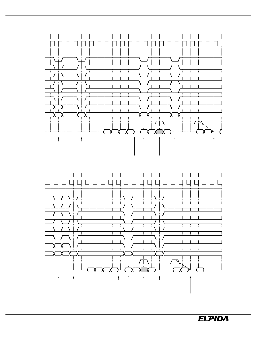
EDL1216AASA
Data Sheet E0196E30 (Ver. 3.0)
49
Read and Write
CLK
CKE
/CS
/RAS
/CAS
/WE
BA1
A10
ADD
DQM
DQ
;;
T0
T1
T2
T3
T4
T5
T6
T7
T8
T9
T10
T11
T12
T13
T14
T15
T16
T17
T18
T19
T20
T21
;
;
;;
;;
;;
;;
;;
;
;;
;;;;
;;;;;
;;;;;
;
;
;;;;
;;;;
;;;;
;;;;
QAa1
QAa2
;;;;;;;;;;;;;
;;;;
;;;;
;;
;;
;;
;;;;
;;;;
;;;;
;;;;
;;
;;;
;;;
;;;
;;;
;;;;;
;;;;;
;;
QAa3
QAa4
DAb1
DAb2
QAc1
QAc2
;
H
RAa
CAc
CAb
;;;;
DAb4
;;
;;
;;
;;
;;
;;
;;
;;
CAa
;
;;;;;
;;;
;;;;
RAa
;
;;
BA0
;;
;;;;
;;;;
;;
;;
;;
;;
;
;;
Activate
Command
for Bank A
Read
Command
for Bank A
Write
Command
for Bank A
0-Clock Latency
Read
Command
for Bank A
Word Masking
Write Latency = 0
L
Hi-Z
Hi-Z at the end of wrap function
2-Clock Latency
[Burst Length = 4, /CAS Latency = 3]
CLK
CKE
/CS
/RAS
/CAS
/WE
BA1
A10
ADD
DQM
DQ
Activate
Command
for Bank A
Read
Command
for Bank A
Write
Command
for Bank A
0-Clock Latency
2-Clock Latency
Read
Command
for Bank A
;
T0
T1
T2
T3
T4
T5
T6
T7
T8
T9
T10
T11
T12
T13
T14
T15
T16
T17
T18
T19
T20
T21
;;
;
;
;
;
;
;
;
;;;;
;;;;
;;
;;
;;;;;
;;;;;
;;;;;
QAa1
QAa2
;;;;
;;;;
;;;
;;;
;;;
;;;;;
;;;;;
;;;;;
;;;;;
;;;;;
;;;
;;;
;;
;;
;;
;;;;
;;;;
;;
;;
QAa3
QAa4
DAb1
DAb2
QAc1
QAc2
QAc4
;;;;;
H
RAa
CAc
CAb
;;;;
;;;;
DAb4
;;
BA0
;
;;;;
;;;;;
;;;
;;;;
;
;
;
;
;
;
;;
;;
CAa
;;
;;
Write Latency = 0
RAa
;;;;
;;;;
;;
;;
;;;;;
;;;;;
Word Masking
L
Hi-Z
Hi-Z at the end of wrap function
[Burst Length = 4, /CAS Latency = 2]
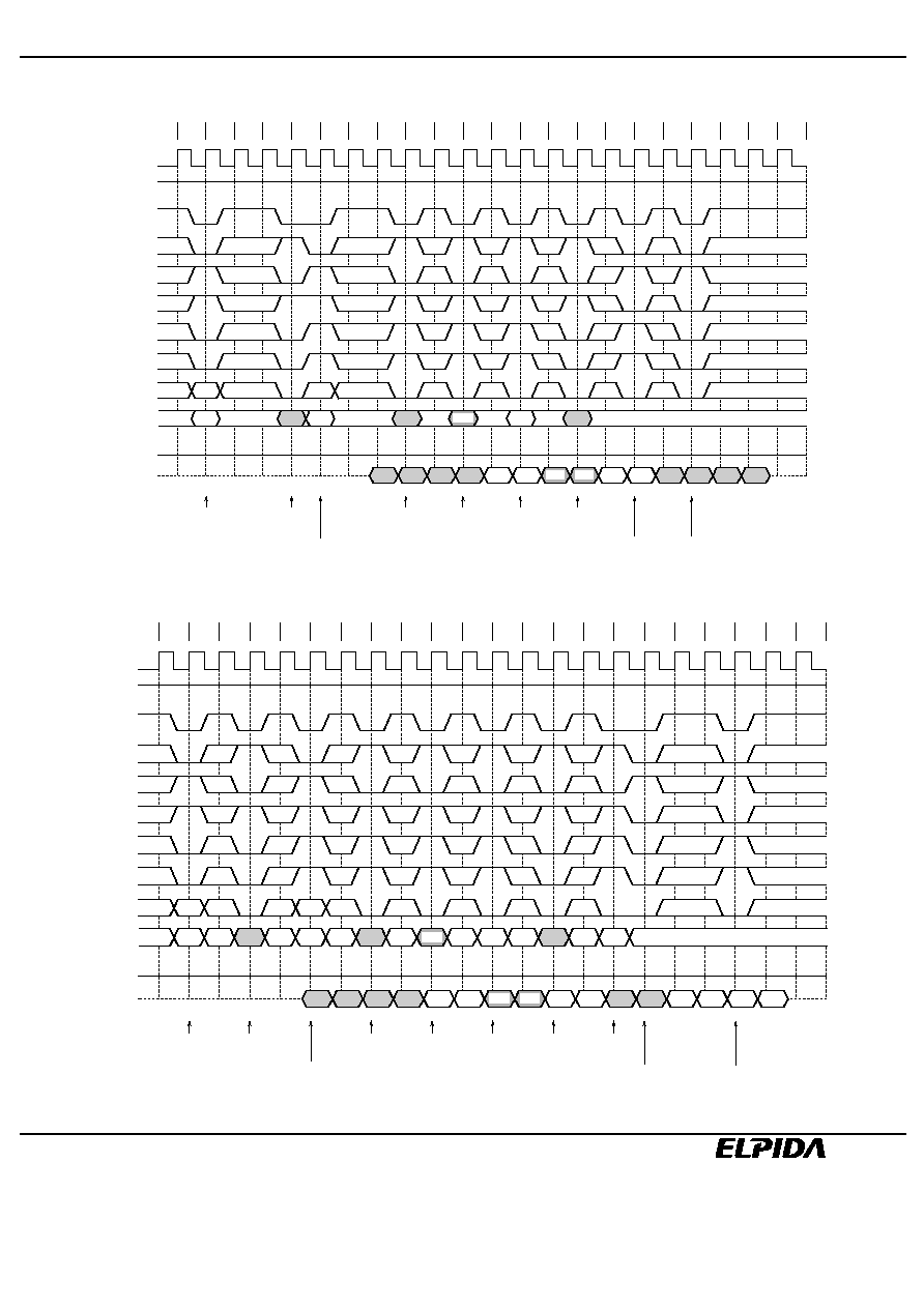
EDL1216AASA
Data Sheet E0196E30 (Ver. 3.0)
50
Interleaved Column Read Cycle
CLK
CKE
/CS
/RAS
/CAS
/WE
BA1
A10
ADD
DQM
DQ
;;
T0
T1
T2
T3
T4
T5
T6
T7
T8
T9
T10
T11
T12
T13
T14
T15
T16
T17
T18
T19
T20
T21
;
;;
;;
;;
;;
;
L
Hi-Z
;;
;;;
;;;
;;;
Aa1
Aa2
;;;;;;;;;;;;
;;
;;
;;
;;
;;
;;
Aa3
Aa4
Da1
Da2
Dc1
Dc2
Ab3
Ab4
;
;
H
;;;;
;;
;;
;;
;;
;;
;
;;
;
;
;;;
;;;
;;
;;
;;
;;
;;
;;
;
;;
;
;;
;;
;;
;
;;
;;
;;
;;
;
;
;
;;
;;
Ab1
Ab2
Db1
Db2
;;
;;
;;
;;
;;
;;
RAa
;;
RDa
;;
;;
;;
;;
;;;
BA0
;;
;;
;;
;;
;;
;;
;;
;;
;;
;;
;;
;;
;;
;
;
;;
;;
;;
;;
;;;
;;;
;;;;;;;;;;;;
;;;;;;;;;;;;
RAa
CAb
CDc
RDa
CDa
CAa
Activate
Command
for Bank A
Activate
Command
for Bank D
Read
Command
for Bank D
Read
Command
for Bank D
Read
Command
for Bank D
Read
Command
for Bank A
Precharge
Command
for Bank D
Precharge
Command
for Bank A
Read
Command
for Bank A
CDb
[Burst Length = 4, /CAS Latency = 3]
CLK
CKE
/CS
/RAS
/CAS
/WE
BA1
A10
ADD
DQM
DQ
;;
T0
T1
T2
T3
T4
T5
T6
T7
T8
T9
T10
T11
T12
T13
T14
T15
T16
T17
T18
T19
T20
T21
;
;;
;;
;;
;
;
;
;
L
Hi-Z
;
;
;;
;;;
;;;
Aa1
Aa2
;;;;
;;
;;
;;
;
;
;
;;
;
;
Aa3
Aa4
Da1
Da2
Dc1
Dc2
Dd1
Dd2
Dd3
Dd4
;
;
H
RAa
RDa
;;
;;
;
;;
;
;;;
;
;
;
;;
;;
;;
;
;;
;;
;
;
;;;
;;
;;
;;
;;
;;
;;
;;
;;
;;
;
;;;
;;;
;;
;;;
;;;
;;
;;
;;
;;
;;
;;
;
;
;
;
;
;;
;
;
;
;
Ab1
Ab2
Db1
Db2
;;
;
;;
;
BA0
;;;;;;
;;
;;
;;
;;
;;
;;
;;;
;
;
;;
;;
RAa
;
;
RDa
CAa
;
CDa
CDb
CDc
CAb
;;;;
;
CDd
;;
;;
;;
;;
;;
;;
Activate
Command
for Bank A
Activate
Command
for bank D
Read
Command
for Bank D
Read
Command
for Bank D
Read
Command
for Bank D
Read
Command
for Bank A
Read
Command
for Bank D
Precharge
Command
for Bank A
Precharge
Command
for Bank D
Read
Command
for Bank A
[Burst Length = 4, /CAS Latency = 2]

EDL1216AASA
Data Sheet E0196E30 (Ver. 3.0)
51
Interleaved Column Write Cycle
CLK
CKE
/CS
/RAS
/CAS
/WE
BA0
A10
ADD
DQM
DQ
;;
;;
T0
T1
T2
T3
T4
T5
T6
T7
T8
T9
T10
T11
T12
T13
T14
T15
T16
T17
T18
T19
T20
T21
;;
;;
;;
;;
;
L
Hi-Z
;;
Aa1
Aa2
;;;;;;;;;;;;
;;
;;
;;
;;
;
;
Aa3
Aa4
Ba1
Ba2
Bc1
Bc2
Bd1
Bd2
;
H
;;;;
;
;;
;;
;;
;;
;
;;
;;
;;
;;
;;
;;
;;
;;
;;
;
;;
;;
;
;
;
Ab1
Ab2
Bb1
Bb2
;;
;;
RAa
;;
RBa
;;
;;
;;
;;
;;
;;
;;
;;
;;;;;;;;;;;;
RAa
CAb
CBc
RBa
CBa
CBb
CAa
;;
;;
;;
;
;
;
;;
;;
;;
;;
;;
;;
;
;;
;
;;
;
;;;;
;;
CBd
Bd3
Bd4
Activate
Command
for Bank A
Write
Command
for Bank A
Activate
Command
for Bank B
Write
Command
for Bank B
Write
Command
for Bank A
Precharge
Command
for Bank A
Precharge
Command
for Bank B
Write
Command
for Bank B
Write
Command
for Bank B
Write
Command
for Bank B
;;
BA1
;
;
;;
;;
;;
;;
;;
;;
;;
;;
;;
;;
;;
;;
;;
;;
;
;
;;
;;
;;
;;
;;
;;
;;
;;
;;
;;
;;
[Burst Length = 4]

EDL1216AASA
Data Sheet E0196E30 (Ver. 3.0)
52
Auto Precharge after Read Burst
CLK
CKE
/CS
/RAS
/CAS
/WE
BA0
A10
ADD
DQM
DQ
;
T0
T1
T2
T3
T4
T5
T6
T7
T8
T9
T10
T11
T12
T13
T14
T15
T16
T17
T18
T19
T20
T21
;
;
;
L
;;;;;;;;;;;;
;;;
;;;
;;;
H
;;;
;;;
;;;
;;;
;
;;
;;
;;
;;
;;
;;
;;;;
;;;
;;;;
;
;;;
;;;;
;;;
;;;;
;;
;;
;;
;;
;;
;
;;
;;
;;
;;
;;
;;;;
;;;;
RDb
;;
;;
;;
;;
;;;
;;;
RAa
;;;;;;;;;;;;
;;;;;;;;;;;;
RAa
CAb
CAa
RDb
CDa
RDa
CDb
Hi-Z
;;
;
BA1
;;
;;;;
;;
;;
;;
;;;;
;;
;;
RDa
Activate
Command
for Bank A
Activate
Command
for Bank D
Read
Command
for Bank A
Read with
Auto Precharge
Command
for Bank D
Read with
Auto Precharge
Command
for Bank A
Read with
Auto Precharge
Command
for Bank D
Auto Precharge
Start for Bank D
Activate
Command
for Bank D
Auto Precharge
Start for Bank A
[Burst Length = 4, /CAS Latency = 3]
CLK
CKE
/CS
/RAS
/CAS
/WE
BA0
A10
ADD
DQM
DQ
;;
T0
T1
T2
T3
T4
T5
T6
T7
T8
T9
T10
T11
T12
T13
T14
T15
T16
T17
T18
T19
T20
T21
;;
;;;
;;
;;
;;;
;;
L
;;;;;;;;;;;
;;
;;
;;;
;;;
;;;
;
;
H
;;
;;
;;;
;;
;;
;;
;;
;;
;
;;
;;
;;
;;
;;
;
;;
;;
;;
;;
;;
;;
;;;;
;;
;;
;;
;;
;;
;;
;;;
;
;;
;;;;
;;
;;
;;
;;
;;
;;;;
;;
;;
;;
;;
;;
;
BA1
;;
;;
;;;;
;;;
;
;;
;;
;
;;
;;
;
;;;
;;
;;
;;
;;
;;
;;
;;
;;
;;
RDb
;;
;;
RAc
;;
;;
;;;
;;;
RDa
;;;
;;;
RAa
;;;;;;;;;;;;
;;;;;;;;;;;;
RAa
CAb
CAa
RDb
CDa
RDa
CAc
CDb
RAc
Hi-Z
Activate
Command
for Bank A
Activate
Command
for Bank D
Read
Command
for Bank A
Read with
Auto Precharge
Command
for Bank D
Read with
Auto Precharge
Command
for Bank A
Auto Precharge
Start for Bank D
Read with
Auto Precharge
Command
for Bank D
Auto Precharge
Start for Bank A
Auto Precharge
Start for Bank D
Activate
Command
for Bank A
Read with
Auto Precharge
Command
for Bank A
Activate
Command
for Bank D
[Burst Length = 4, /CAS Latency = 2]
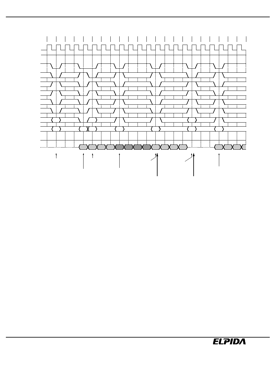
EDL1216AASA
Data Sheet E0196E30 (Ver. 3.0)
53
Auto Precharge after Write Burst
CLK
CKE
/CS
/RAS
/CAS
/WE
BA0
A10
ADD
DQM
DQ
;;
T0
T1
T2
T3
T4
T5
T6
T7
T8
T9
T10
T11
T12
T13
T14
T15
T16
T17
T18
T19
T20
T21
;;
L
;;;;;;;;;;;;;
;;
H
;;;;
;;
;;
;;;;
;;;;
;;;
;;
;;
;;
;;
;;
;;
;;
;;
;;
;;
;;
;;
;;;
;;;
;;
;;
;
;;
;;
;;;
;;;
;;;;
;;;;
RDb
;
;
;;;
;;;
;;;
;;;
RAa
;;;;;;;;;;;;
RAa
CAb
CAa
RDb
CDa
RDa
CDb
;;;
;;
RDa
;;
BA1
;;
;;
;;;
;;;
;;;
;;;
;;
;;
;;
;;
;;
;;
;
;;
;;
;
;;
;;;;
;;;;
;;;
Hi-Z
Activate
Command
for Bank A
Write
Command
for Bank A
Activate
Command
for Bank D
Write with
Auto Precharge
Command
for Bank D
Write with
Auto Precharge
Command
for Bank A
Auto Precharge
Start for Bank D
Auto Precharge
Start for Bank A
Activate
Command
for bank D
Write with
Auto Precharge
Command
for Bank D
[Burst Length = 4]

EDL1216AASA
Data Sheet E0196E30 (Ver. 3.0)
54
Burst Write Operation
CLK
CKE
/CS
/RAS
/CAS
/WE
BA0
A10
ADD
LDQM
;
;
T0
T1
T2
T3
T4
T5
T6
T7
T8
T9
T10
T11
T12
T13
T14
T15
T16
T17
T18
T19
T20
T21
;;;;;
;;;;;
;;;
;;;
;;
;;
;;;
;;;
UDQM
;;;;;
;;;;;
BA1
DQ
(lower)
DQ
(upper)
Activate
Command
for Bank D
Read
Command
for Bank D
Read
Command
for Bank D
;;;
;
;
;;;;;
;;;;;
;;;
;;;
;;
;;
;;;;;
;;;;;
;
;;
;;;;;
;;;
;;;;;
;;;;;;
;;;
;;;;;
;;
;
;
;;;;;
;;;;;
;;;
;;;
;;;;;
;;;;;
;;
;;
;;
;;
;;
;;
;;
;;
;;;;;
;;;
;;;;;
;;
Upper
Byte
not Read
Lower
Byte
not Read
Lower
Byte
not Read
Lower
Byte
not Read
Lower
Byte
not Write
Upper
Byte
not Write
Lower
Byte
not Write
;;;;;;;;;;;;
;;;;;;;;;;;;
;;;;;;;;;;;;
;;;;;;;;;;;;
;
;
;
[Burst Length = 4]
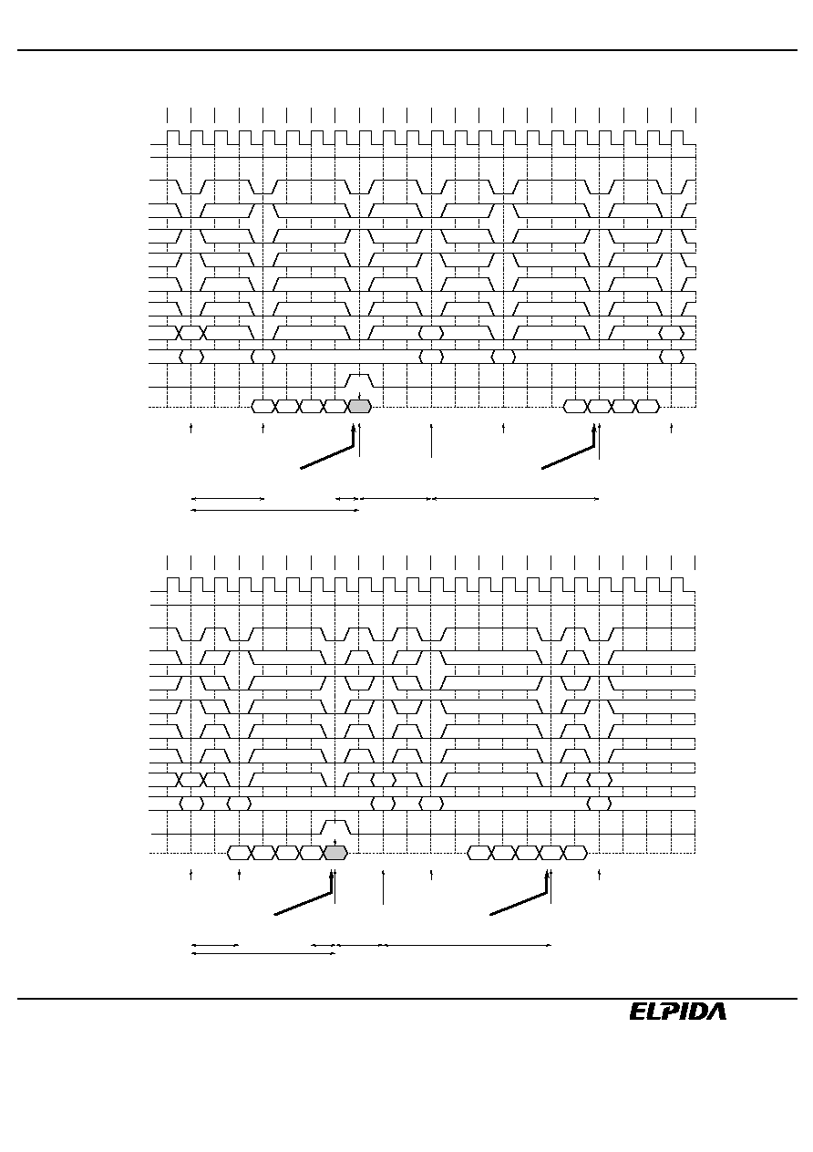
EDL1216AASA
Data Sheet E0196E30 (Ver. 3.0)
55
Precharge Termination
CLK
CKE
/CS
/RAS
/CAS
/WE
BA0
A10
ADD
DQM
DQ
;;
;;
T0
T1
T2
T3
T4
T5
T6
T7
T8
T9
T10
T11
T12
T13
T14
T15
T16
T17
T18
T19
T20
T21
;;
L
Hi-Z
;;;;;;;;;;;;
H
;;
;;
;;
;;
;;
;;
;;
;;;
;;;
;;
;;
;;
;;
;;
;;
;;
;;
;;;
;;;
;;
;;
;;
;;;
;;;
;;
;;;
;;;
;;;
;;;
;;
;;;
BA1
;;
;;
;;;
;;;
;;
;;
;;
;;
;;
;;
;;
;;
;;
;;
;;;;;
;;;;;
;;;
;;;
;;;;;;;;;;;;;
RAa
RAb
CAa
;;;;
;;;;
RAa
RAb
CAb
DAa1
DAa2
DAa3
QAb1 QAb2
QAb3
QAb4
Hi-Z
Activate
Command
for Bank A
Activate
Command
for Bank A
Write
Command
for Bank A
PRE Termination
of Burst
Precharge
Command
for Bank A
Precharge
Command
for Bank A
Activate
Command
for Bank A
Read
Command
for Bank A
PRE Termination
of Burst
;;
;;;
DAa4
DAa5
Write
Masking
;;;
;;
;;
;
;
;;
;;;
;;
;;
RAc
RAc
;
t
RCD
t
RP
t
RAS
t
DPL
t
RAS
[Burst Length = 8, /CAS Latency = 3]
CLK
CKE
/CS
/RAS
/CAS
/WE
BA0
A10
ADD
DQM
DQ
;;
;;
T0
T1
T2
T3
T4
T5
T6
T7
T8
T9
T10
T11
T12
T13
T14
T15
T16
T17
T18
T19
T20
T21
;;
L
;;;;;;;;;;;;
H
;;;
;;;
;;
;;
;;
;;
;;
;;;
;;;
;;
;;
;;
;;
;;;
;;;
;;
;;
;;
;;
;;;
;;;
;;
;;
;;
;;
;;
;;
;;
;;;
;;;
;;
;;
;;
;;;;;
;
;;
;;
;;
;;;
BA1
;
;
;
;
;;;
;;;
;;
;;
;
;
;;
;
;
;;;
;;;
;
;;;;;
;;;;
Hi-Z
;;;;;;;;;;;;
RAa
RAb
CAa
;;;
RAa
RAb
CAb
DAa1
DAa2
DAa3
DAa4
DAa5
QAb1
QAb2
QAb3
QAb4
QAb5
Activate
Command
for Bank A
Activate
Command
for Bank A
Write
Command
for Bank A
PRE Termination
of Burst
PRE Termination
of Burst
Precharge
Command
for Bank A
Activate
Command
for Bank A
Read
Command
for Bank A
Precharge
Command
for Bank A
Hi-Z
Write
Masking
;
;
;
;
;
;;
RAc
RAc
t
RCD
t
DPL
t
RP
t
RAS
t
RAS
[Burst Length = 8, /CAS Latency = 2]
EDL1216AASA
Data Sheet E0196E30 (Ver. 3.0)
56
Package Drawing
54-ball FBGA (
µ
µ
µ
µ
BGA)
Solder ball: Lead free (Sn-Ag-Cu)
8.0
±
0.1
//
0.2 S
0.1 S
0.35
±
0.05
1.0 max
S
8.0
±
0.1
0.2 S A
0.2 S B
A B C D E F G H J
1 2 3
7 8 9
0.8
1.6
B
0.8
0.8
0.8
A
54-
0.45
±
0.05
0.08
M
S A B
INDEX AREA
INDEX MARK
Unit: mm
ECA-TS2-0017-04

EDL1216AASA
Data Sheet E0196E30 (Ver. 3.0)
57
Recommended Soldering Conditions
Please consult with our sales offices for soldering conditions of the EDL1216AASA.
Type of Surface Mount Device
EDL1216AASA: 54-ball FBGA (
µ
BGA) < Lead free (Sn-Ag-Cu) >
EDL1216AASA
Data Sheet E0196E30 (Ver. 3.0)
58
NOTES FOR CMOS DEVICES
1
PRECAUTION AGAINST ESD FOR MOS DEVICES
Exposing the MOS devices to a strong electric field can cause destruction of the gate
oxide and ultimately degrade the MOS devices operation. Steps must be taken to stop
generation of static electricity as much as possible, and quickly dissipate it, when once
it has occurred. Environmental control must be adequate. When it is dry, humidifier
should be used. It is recommended to avoid using insulators that easily build static
electricity. MOS devices must be stored and transported in an anti-static container,
static shielding bag or conductive material. All test and measurement tools including
work bench and floor should be grounded. The operator should be grounded using
wrist strap. MOS devices must not be touched with bare hands. Similar precautions
need to be taken for PW boards with semiconductor MOS devices on it.
2
HANDLING OF UNUSED INPUT PINS FOR CMOS DEVICES
No connection for CMOS devices input pins can be a cause of malfunction. If no
connection is provided to the input pins, it is possible that an internal input level may be
generated due to noise, etc., hence causing malfunction. CMOS devices behave
differently than Bipolar or NMOS devices. Input levels of CMOS devices must be fixed
high or low by using a pull-up or pull-down circuitry. Each unused pin should be connected
to V
DD
or GND with a resistor, if it is considered to have a possibility of being an output
pin. The unused pins must be handled in accordance with the related specifications.
3
STATUS BEFORE INITIALIZATION OF MOS DEVICES
Power-on does not necessarily define initial status of MOS devices. Production process
of MOS does not define the initial operation status of the device. Immediately after the
power source is turned ON, the MOS devices with reset function have not yet been
initialized. Hence, power-on does not guarantee output pin levels, I/O settings or
contents of registers. MOS devices are not initialized until the reset signal is received.
Reset operation must be executed immediately after power-on for MOS devices having
reset function.
CME0107

EDL1216AASA
Data Sheet E0196E30 (Ver. 3.0)
59
µ
BGA is a registered trademark of Tessera, Inc.
M01E0107
No part of this document may be copied or reproduced in any form or by any means without the prior
written consent of Elpida Memory, Inc.
Elpida Memory, Inc. does not assume any liability for infringement of any intellectual property rights
(including but not limited to patents, copyrights, and circuit layout licenses) of Elpida Memory, Inc. or
third parties by or arising from the use of the products or information listed in this document. No license,
express, implied or otherwise, is granted under any patents, copyrights or other intellectual property
rights of Elpida Memory, Inc. or others.
Descriptions of circuits, software and other related information in this document are provided for
illustrative purposes in semiconductor product operation and application examples. The incorporation of
these circuits, software and information in the design of the customer's equipment shall be done under
the full responsibility of the customer. Elpida Memory, Inc. assumes no responsibility for any losses
incurred by customers or third parties arising from the use of these circuits, software and information.
[Product applications]
Elpida Memory, Inc. makes every attempt to ensure that its products are of high quality and reliability.
However, users are instructed to contact Elpida Memory's sales office before using the product in
aerospace, aeronautics, nuclear power, combustion control, transportation, traffic, safety equipment,
medical equipment for life support, or other such application in which especially high quality and
reliability is demanded or where its failure or malfunction may directly threaten human life or cause risk
of bodily injury.
[Product usage]
Design your application so that the product is used within the ranges and conditions guaranteed by
Elpida Memory, Inc., including the maximum ratings, operating supply voltage range, heat radiation
characteristics, installation conditions and other related characteristics. Elpida Memory, Inc. bears no
responsibility for failure or damage when the product is used beyond the guaranteed ranges and
conditions. Even within the guaranteed ranges and conditions, consider normally foreseeable failure
rates or failure modes in semiconductor devices and employ systemic measures such as fail-safes, so
that the equipment incorporating Elpida Memory, Inc. products does not cause bodily injury, fire or other
consequential damage due to the operation of the Elpida Memory, Inc. product.
[Usage environment]
This product is not designed to be resistant to electromagnetic waves or radiation. This product must be
used in a non-condensing environment.
If you export the products or technology described in this document that are controlled by the Foreign
Exchange and Foreign Trade Law of Japan, you must follow the necessary procedures in accordance
with the relevant laws and regulations of Japan. Also, if you export products/technology controlled by
U.S. export control regulations, or another country's export control laws or regulations, you must follow
the necessary procedures in accordance with such laws or regulations.
If these products/technology are sold, leased, or transferred to a third party, or a third party is granted
license to use these products, that third party must be made aware that they are responsible for
compliance with the relevant laws and regulations.
The information in this document is subject to change without notice. Before using this document, confirm that this is the latest version.