Document Outline
- COVER
- Description
- Features
- Ordering Information
- Part Number
- Pin Configurations
- Electrical Specifications
- Absolute Maximum Ratings
- Recommended Operating Conditions
- DC Characteristics
- Pin Capacitance
- AC Characteristics
- Test Conditions
- Relationship Between Frequency and Minimum Latency
- Block Diagram
- Pin Function
- Command Operation
- Truth Table
- Command Truth Table
- DQM Truth Table
- CKE Truth Table
- Function Truth Table
- Command Truth Table for CKE
- Simplified State Diagram
- Programming Mode Registers
- Mode Register
- Burst Length and Sequence
- Address Bits of Bank-Select and Precharge
- Power-up sequence
- Operation of the SDRAM
- Read/Write Operations
- Auto Precharge
- Command Intervals
- DQM Control
- Refresh
- Others
- Timing Waveforms
- Read Cycle
- Write Cycle
- Mode Register Set Cycle
- Read Cycle/Write Cycle
- Read/Single Write Cycle
- Read/Burst Write Cycle
- Auto Refresh Cycle
- Self Refresh Cycle
- Clock Suspend Mode
- Power Down Mode
- Initialization Sequence
- Package Drawing
- 90-ball FBGA
- 86-pin TSOP(II)
- Recommended Soldering Conditions

Document No. E0247E40 (Ver. 4.0)
Date Published July 2002 (K) Japan
URL: http://www.elpida.com
Elpida Memory, Inc. 2002
PRELIMINARY DATA SHEET
128M bits SDRAM
EDS1232CABB, EDS1232CATA (4M words
◊
◊
◊
◊
32 bits)
Description
The EDS1232CA is a 128M bits SDRAM organized as
1,048,576 words
◊
32 bits
◊
4 banks. All inputs and
outputs are synchronized with the positive edge of the
clock.
They are packaged in 90-ball FBGA, 86-pin plastic
TSOP (II).
Features
∑
2.5V power supply
∑
Clock frequency: 133MHz (max.)
∑
Single pulsed /RAS
∑ ◊
32 organization
∑
4 banks can operate simultaneously and
independently
∑
Burst read/write operation and burst read/single write
operation capability
∑
Programmable burst length (BL): 1, 2, 4, 8 and full
page
∑
2 variations of burst sequence
Sequential (BL = 1, 2, 4, 8)
Interleave (BL = 1, 2, 4, 8)
∑
Programmable /CAS latency (CL): 2, 3
∑
Byte control by DQM
∑
Refresh cycles: 4096 refresh cycles/64ms
∑
2 variations of refresh
Auto refresh
Self refresh
∑
FBGA package is lead free solder (Sn-Ag-Cu)
EDS1232CABB, EDS1232CATA
Preliminary Data Sheet E0247E40 (Ver. 4.0)
2
Ordering Information
Part number
Supply
voltage
Organization
(words
◊
bits)
Internal Banks
Clock frequency
MHz (max.)
/CAS latency
Package
EDS1232CABB-75-E 2.5V
4M
◊
32
4
133
3
90-ball FBGA
EDS1232CABB-1A-E
100
2,
3
EDS1232CABB-75L-E
133
3
EDS1232CABB-1AL-E
100
2,
3
EDS1232CATA-75 2.5V 4M
◊
32
4
133
3
86-pin plastic
EDS1232CATA-1A
100
2, 3
TSOP (II)
EDS1232CATA-75L
133
3
EDS1232CATA-1AL
100
2,
3
Part Number
Lead Free
Elpida Memory
Density / Bank
12: 128M/4 Banks
Bit Organization
32: x32
Voltage, Interface
C: 2.5V, LVTTL
Die Revision
Package
TA: TSOP (II)
BB: FBGA
Speed
75: 133MHz/CL3
100MHz/CL2
1A: 100MHz/CL2,3
Power Consumption
Blank: Normal
L: Low Power
Product Code
S: SDRAM
Type
D: Monolithic Device
E D S 12 32 C A BB - 75 L - E
EDS1232CABB, EDS1232CATA
Preliminary Data Sheet E0247E40 (Ver. 4.0)
3
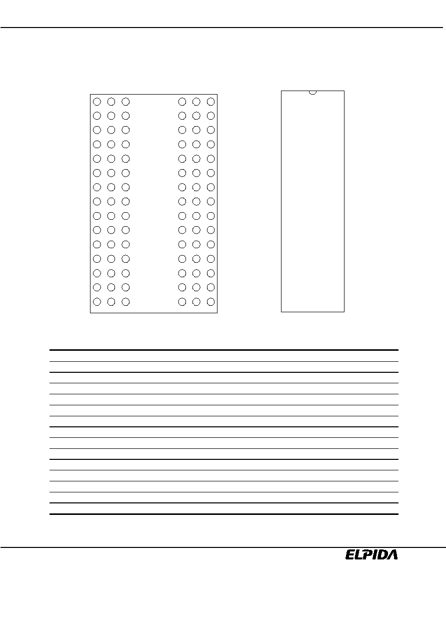
Pin Configurations
/xxx indicate active low signal.
DQ26
1
A
B
C
D
E
F
G
H
J
K
L
M
N
P
R
2
3
4
5
6
7
8
9
DQ28
VSSQ
VSSQ
VDDQ
VSS
A4
A7
CLK
DQ24
VDDQ
DQ27
DQ29
DQ31
DQM3
A5
A8
CKE
VSS
VSSQ
DQ25
DQ30
NC
A3
A6
NC
A9
VDD
VDDQ
DQ22
DQ17
NC
A2
A10
NC
BA0
DQ23
VSSQ
DQ20
DQ18
DQ16
DQM2
A0
BA1
/CS
DQ21
DQ19
VDDQ
VDDQ
VSSQ
VDD
A1
A11
/RAS
(Top view)
(Top view)
DQM1
NC
NC
/CAS
/WE DQM0
VDDQ DQ8
VSS
VDD
DQ7 VSSQ
VSSQ DQ10 DQ9
DQ6
DQ5 VDDQ
VSSQ DQ12 DQ14
DQ1
DQ3 VDDQ
DQ11 VDDQ VSSQ
VDDQ VSSQ DQ4
DQ13 DQ15 VSS
VDD
DQ0
DQ2
1
2
3
4
5
6
7
8
9
10
11
12
13
14
15
16
17
18
19
20
21
22
23
24
25
26
27
28
29
30
31
32
33
34
35
36
37
38
39
40
41
42
43
86
85
84
83
82
81
80
79
78
77
76
75
74
73
72
71
70
69
68
67
66
65
64
63
62
61
60
59
58
57
56
55
54
53
52
51
50
49
48
47
46
45
44
VSS
DQ15
VSSQ
DQ14
DQ13
VDDQ
DQ12
DQ11
VSSQ
DQ10
DQ9
VDDQ
DQ8
NC
VSS
DQM1
NC
NC
CLK
CKE
A9
A8
A7
A6
A5
A4
A3
DQM3
VSS
NC
DQ31
VDDQ
DQ30
DQ29
VSSQ
DQ28
DQ27
VDDQ
DQ26
DQ25
VSSQ
DQ24
VSS
VDD
DQ0
VDDQ
DQ1
DQ2
VSSQ
DQ3
DQ4
VDDQ
DQ5
DQ6
VSSQ
DQ7
NC
VDD
DQM0
/WE
/CAS
/RAS
/CS
A11
BA0
BA1
A10(AP)
A0
A1
A2
DQM2
VDD
NC
DQ16
VSSQ
DQ17
DQ18
VDDQ
DQ19
DQ20
VSSQ
DQ21
DQ22
VDDQ
DQ23
VDD
86-pin TSOP
90-ball FBGA
Pin name
Function
A0 to A11
Address inputs
BA0, BA1
Bank select
DQ0 to DQ31
Data input/output
CLK Clock
input
CKE Clock
enable
/CS Chip
select
/RAS
Row address strobe
/CAS Column
address
strobe
/WE Write
enable
DQM0 to DQM3
DQ mask enable
VDD Supply
voltage
VSS Ground
VDDQ
Supply voltage for DQ
VSSQ
Ground for DQ
NC No
connection
EDS1232CABB, EDS1232CATA
Preliminary Data Sheet E0247E40 (Ver. 4.0)
4
CONTENTS
Description .................................................................................................................................................... 1
Features ........................................................................................................................................................ 1
Ordering Information ..................................................................................................................................... 2
Part Number.................................................................................................................................................. 2
Pin Configurations......................................................................................................................................... 3
Electrical Specifications ................................................................................................................................ 5
Block Diagram............................................................................................................................................. 10
Pin Function ................................................................................................................................................ 11
Command Operation................................................................................................................................... 12
Truth Table.................................................................................................................................................. 16
Simplified State Diagram ............................................................................................................................ 22
Programming Mode Registers .................................................................................................................... 23
Mode Register............................................................................................................................................. 24
Power-up sequence .................................................................................................................................... 27
Operation of the SDRAM ............................................................................................................................ 28
Timing Waveforms ...................................................................................................................................... 44
Package Drawing........................................................................................................................................ 51
Recommended Soldering Conditions ......................................................................................................... 53
Revision History .......................................................................................................................................... 56
EDS1232CABB, EDS1232CATA
Preliminary Data Sheet E0247E40 (Ver. 4.0)
5
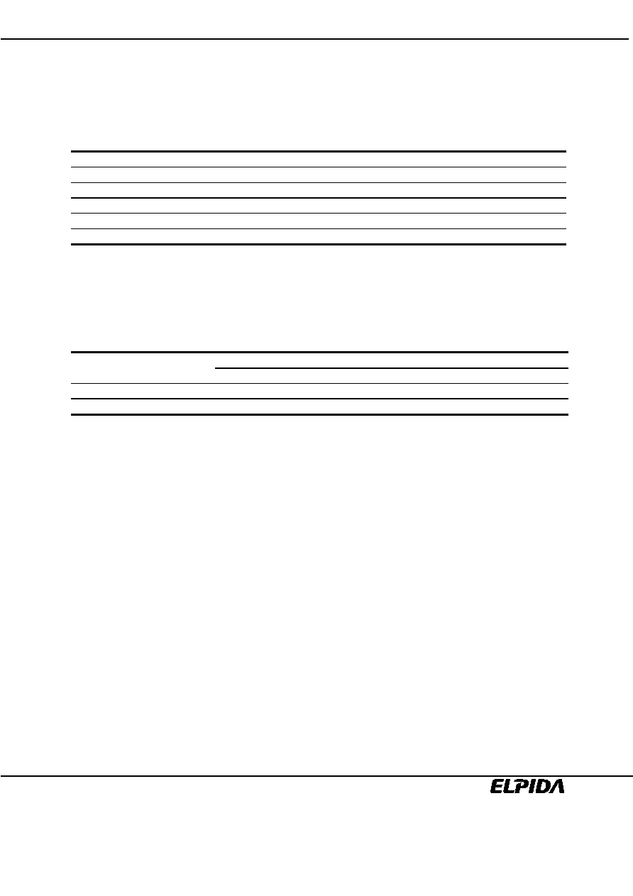
Electrical Specifications
∑
All voltages are referenced to VSS (GND).
∑
After power up (refer to the Power up sequence).
Absolute Maximum Ratings
Parameter Symbol
Rating
Unit
Note
Voltage on any pin relative to VSS
VT
≠0.5 to +3.6
V
Supply voltage relative to VSS
VDD, VDDQ
≠0.5 to +3.6
V
Short circuit output current
IOS
50
mA
Power dissipation
PD
1.0
W
Operating ambient temperature
TA
0 to +70
∞
C
Storage temperature
Tstg
≠55 to +125
∞
C
Caution
Exposing the device to stress above those listed in Absolute Maximum Ratings could cause
permanent damage. The device is not meant to be operated under conditions outside the limits
described in the operational section of this specification. Exposure to Absolute Maximum Rating
conditions for extended periods may affect device reliability.
Recommended Operating Conditions (TA = 0 to +70
∞
∞
∞
∞
C)
Parameter Symbol
min.
typ.
max.
Unit
Notes
Supply
voltage
VDD,
VDDQ
2.3 2.5 2.7 V
VSS
0 0 0 V
Input high voltage
VIH
1.7
VDD
+
0.3*
1
V
Input low voltage
VIL
≠0.3
0.7 V
Notes: 1. VIH (max.) = VDDQ + 1.5V (pulse width
5ns).
2. VIL (min.) = ≠1.5V (pulse width
5ns).