Document Outline
- COVER
- Description
- Features
- Pin Configurations
- Ordering Information
- Part Number
- Electrical Specifications
- Absolute Maximum Ratings
- Recommended DC Operating Conditions
- DC Characteristics 1
- DC Characteristics 2
- Pin Capacitance
- AC Characteristics
- Test Conditions
- Relationship Between Frequency and Minimum Latency
- Block Diagram
- Pin Function
- Command Operation
- Command Truth Table
- DQM Truth Table
- CKE Truth Table
- Function Truth Table
- Command Truth Table for CKE
- Simplified State Diagram
- Mode Register Configuration
- Power-up sequence
- Power-up sequence
- Initialization sequence
- Operation of the SDRAM
- Read/Write Operations
- Auto Precharge
- Burst Stop Command
- Command Intervals
- DQM Control
- Refresh
- Others
- Timing Waveforms
- Read Cycle
- Write Cycle
- Mode Register Set Cycle
- Read Cycle/Write Cycle
- Read/Single Write Cycle
- Read/Burst Write Cycle
- Auto Refresh Cycle
- Self Refresh Cycle
- Clock Suspend Mode
- Power Down Mode
- Initialization Sequence
- Package Drawing
- Recommended Soldering Conditions
Document No. E0396E10 (Ver. 1.0)
Date Published June 2003 (K) Japan
URL: http://www.elpida.com
Elpida Memory, Inc. 2003
PRELIMINARY DATA SHEET
256M bits SDRAM
EDS2732AABH (8M words
◊
◊
◊
◊
32 bits)
Description
The EDS2732AA is a 256M bits SDRAM organized as
2,097,152 words
◊
32 bits
◊
4 banks. All inputs and
outputs are synchronized with the positive edge of the
clock.
It is packaged in 90-ball FBGA.
Features
∑
3.3V power supply
∑
Clock frequency: 166MHz/133MHz (max.)
∑
Single pulsed /RAS
∑ ◊
32 organization
∑
4 banks can operate simultaneously and
independently
∑
Burst read/write operation and burst read/single write
operation capability
∑
Programmable burst length (BL): 1, 2, 4, 8 and full
page
∑
2 variations of burst sequence
Sequential (BL = 1, 2, 4, 8, full page)
Interleave (BL = 1, 2, 4, 8)
∑
Programmable /CAS latency (CL): 2, 3
∑
Byte control by DQM
∑
Address
8K Row address /256 column address
∑
Refresh cycles
4096 refresh cycles/64ms
∑
2 variations of refresh
Auto refresh
Self refresh
∑
FBGA package is lead free solder (Sn-Ag-Cu)
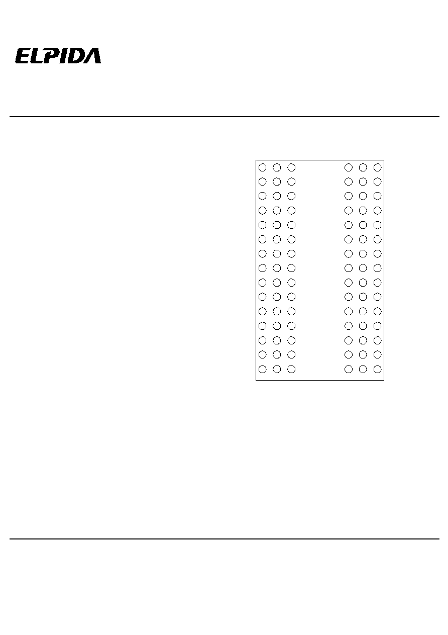
Pin Configurations
/xxx indicate active low signal.
DQ26
1
A
B
C
D
E
F
G
H
J
K
L
M
N
P
R
2
3
4
5
6
7
8
9
DQ28
VSSQ
VSSQ
VDDQ
VSS
A4
A7
CLK
DQ24
VDDQ
DQ27
DQ29
DQ31
DQM3
A5
A8
CKE
VSS
VSSQ
DQ25
DQ30
NC
A3
A6
A12
A9
VDD
VDDQ
DQ22
DQ17
NC
A2
A10
NC
BA0
DQ23
VSSQ
DQ20
DQ18
DQ16
DQM2
A0
BA1
/CS
DQ21
DQ19
VDDQ
VDDQ
VSSQ
VDD
A1
A11
/RAS
(Top view)
DQM1
NC
NC
/CAS
/WE DQM0
VDDQ DQ8
VSS
VDD
DQ7 VSSQ
VSSQ DQ10 DQ9
DQ6
DQ5 VDDQ
VSSQ DQ12 DQ14
DQ1
DQ3 VDDQ
DQ11 VDDQ VSSQ
VDDQ VSSQ DQ4
DQ13 DQ15 VSS
VDD
DQ0
DQ2
90-ball FBGA
Address inputs
Bank select address
Data-input/output
Chip select
Row address strobe
Column address strobe
Write enable
DQ mask enable
Clock enable
Clock input
Power for internal circuit
Ground for internal circuit
Power for DQ circuit
Ground for DQ circuit
No connection
A0 to A12
BA0, BA1
DQ0 to DQ31
/CS
/RAS
/CAS
/WE
DQM0 to DQM3
CKE
CLK
VDD
VSS
VDDQ
VSSQ
NC
EDS2732AABH
Preliminary Data Sheet E0396E10 (Ver. 1.0)
2
Ordering Information
Part number
Supply
voltage
Organization
(words
◊
bits)
Internal Banks
Clock frequency
MHz (max.)
/CAS latency
Package
EDS2732AABH-60-E
3.3V
8M
◊
32
4
166
133
3
2
90-ball FBGA
EDS2732AABH-75-E
133
100
3
2
EDS2732AABH-60L-E
166
133
3
2
EDS2732AABH-75L-E
133
100
3
2
Part Number
Environment Code
Blank: Sn-Pb Solder
E: Lead Free
Elpida Memory
Density / Bank
27: 256M/4-bank, 8K Rows
Bit Organization
32: x32
Voltage, Interface
A: 3.3V, LVTTL
Die Rev.
Package
BH: FBGA(Board Type)
Speed
60: 166MHz/CL3
133MHz/CL2
75: 133MHz/CL3
100MHz/CL2
Power Consumption
Blank: Normal
L: Low Power
Product Code
S: SDRAM
Type
D: Monolithic Device
E D S 27 32 A A BH - 60 L - E
EDS2732AABH
Preliminary Data Sheet E0396E10 (Ver. 1.0)
3
CONTENTS
Description .................................................................................................................................................... 1
Features ........................................................................................................................................................ 1
Pin Configurations ......................................................................................................................................... 1
Ordering Information ..................................................................................................................................... 2
Part Number .................................................................................................................................................. 2
Electrical Specifications................................................................................................................................. 4
Block Diagram ............................................................................................................................................... 9
Pin Function ................................................................................................................................................ 10
Command Operation ................................................................................................................................... 11
Simplified State Diagram............................................................................................................................. 19
Mode Register Configuration ...................................................................................................................... 20
Power-up sequence .................................................................................................................................... 22
Operation of the SDRAM ............................................................................................................................ 23
Timing Waveforms ...................................................................................................................................... 39
Package Drawing ........................................................................................................................................ 45
Recommended Soldering Conditions.......................................................................................................... 46

EDS2732AABH
Preliminary Data Sheet E0396E10 (Ver. 1.0)
4
Electrical Specifications
∑
All voltages are referenced to VSS (GND).
∑
After power up, execute power up sequence and initialization sequence before proper device operation is achieved
(refer to the Power up sequence).
Absolute Maximum Ratings
Parameter
Symbol
Rating
Unit
Note
Voltage on any pin relative to VSS
VT
≠0.5 to VDD + 0.5 ( 4.6 (max.))
V
Supply voltage relative to VSS
VDD
≠0.5 to +4.6
V
Short circuit output current
IOS
50
mA
Power dissipation
PD
1.0
W
Operating temperature
TA
0 to +70
∞
C
Storage temperature
Tstg
≠55 to +125
∞
C
Caution
Exposing the device to stress above those listed in Absolute Maximum Ratings could cause
permanent damage. The device is not meant to be operated under conditions outside the limits
described in the operational section of this specification. Exposure to Absolute Maximum Rating
conditions for extended periods may affect device reliability.
Recommended DC Operating Conditions (TA = 0 to +70
∞
∞
∞
∞
C)
Parameter
Symbol
min.
max.
Unit
Notes
Supply voltage
VDD, VDDQ
3.0
3.6
V
1
VSS, VSSQ
0
0
V
2
Input high voltage
VIH
2.0
VDD + 0.3
V
3
Input low voltage
VIL
≠0.3
0.8
V
4
Notes: 1. The supply voltage with all VDD
and VDDQ pins must be on the same level.
2. The supply voltage with all VSS and VSSQ pins must be on the same level.
3. VIH (max.) = VDD + 1.5V (pulse width 5ns).
4. VIL (min.) = VSS ≠ 1.5V (pulse width 5ns).
EDS2732AABH
Preliminary Data Sheet E0396E10 (Ver. 1.0)
5
DC Characteristics 1 (TA = 0 to +70
∞
∞
∞
∞
C, VDD, VDDQ = 3.3V ± 0.3V, VSS, VSSQ = 0V)
Parameter
/CAS latency
Symbol
Grade
max.
Unit
Test condition
Notes
Operating current
IDD1
-60
-75
110
105
mA
Burst length = 1
tRC = tRC (min.)
1, 2, 3
Standby current in power down
IDD2P
3
mA
CKE = VIL,
tCK = tCK (min.)
6
Standby current in power down
(input signal stable)
IDD2PS
2
mA
CKE = VIL, tCK =
7
Standby current in non power
down
IDD2N
20
mA
CKE, /CS = VIH,
tCK = tCK (min.)
4
Standby current in non power
down (input signal stable)
IDD2NS
9
mA
CKE = VIH, tCK =
,
/CS = VIH
8
Active standby current in power
down
IDD3P
4
mA
CKE = VIL,
tCK = tCK (min.)
1, 2, 6
Active standby current in power
down (input signal stable)
IDD3PS
3
mA
CKE = VIL, tCK =
2, 7
Active standby current in non
power down
IDD3N
45
mA
CKE, /CS = VIH,
tCK = tCK (min.)
1, 2, 4
Active standby current in non
power down (input signal stable)
IDD3NS
30
mA
CKE = VIH, tCK =
,
/CS = VIH
2, 8
Burst operating current
IDD4
-60
-75
180
150
mA
tCK = tCK (min.),
BL = 4
1, 2, 5
Refresh current
IDD5
-60
-75
300
270
mA
tRC = tRC (min.)
3
Self refresh current
IDD6
3
mA
VIH VDD ≠ 0.2V
VIL 0.2V
Self refresh current
(L-version)
IDD6
-XXL
1
mA
VIH VDD ≠ 0.2V
VIL 0.2V
Notes: 1. IDD depends on output load condition when the device is selected. IDD (max.) is specified at the output
open condition.
2. One bank operation.
3. Input signals are changed once per one clock.
4. Input signals are changed once per two clocks.
5. Input signals are changed once per four clocks.
6. After power down mode, CLK operating current.
7. After power down mode, no CLK operating current.
8. Input signals are VIH or VIL fixed.