Document Outline
- ˛ˇ
- ˛ˇ
- ˛ˇ
- ˛ˇ
- ˛ˇ
- ˛ˇ
- ˛ˇ
- ˛ˇ
- ˛ˇ
- ˛ˇ
- ˛ˇ
- ˛ˇ
- ˛ˇ
- ˛ˇ
- ˛ˇ
- ˛ˇ
- ˛ˇ
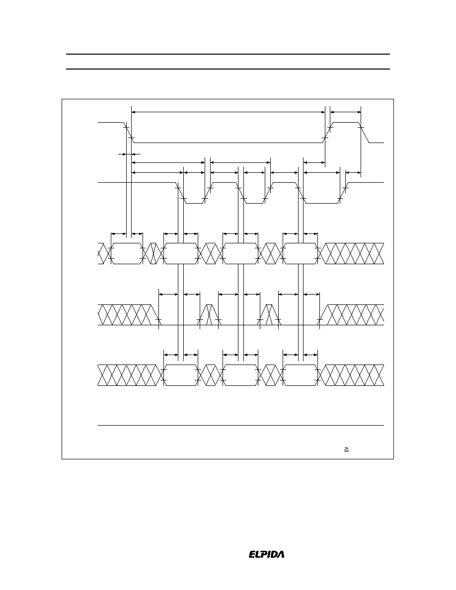
- /RAS-Only Refresh Cycle
- /CAS-Before-/RAS Refresh Cycle
- ˛ˇ
- ˛ˇ
- ˛ˇ
- ˛ˇ
- ˛ˇ
- ˛ˇ
- ˛ˇ
- ˛ˇ
- ˛ˇ
EOL Product
Elpida Memory, Inc. is a joint venture DRAM company of NEC Corporation and Hitachi, Ltd.
HM5117805 Series
16 M EDO DRAM (2-Mword
◊
8-bit)
2 k Refresh
E0156H10 (Ver. 1.0)
(Previous ADE-203-630D (Z))
Jun. 27, 2001
Description
The HM 5117805 i s a C M OS dynam i c R AM orga ni ze d 2, 097,152-w ord
◊
8-bi t . It em pl oys t he m os t
adva nce d C M OS t ec hnology for hi gh per form a nce and l ow powe r. The HM 5117805 off ers Ext ende d Da ta
Out (ED O) P age M ode as a hi gh s pee d ac ce s s m ode. M ul ti pl exe d addr es s i nput per m it s t he HM 5117805 t o
be packaged in standard 28-pin plastic SOJ and 28-pin TSOP.
Features
∑
Single 5 V (±10%)
∑
Access time: 50 ns/60 ns/70 ns (max)
∑
Power dissipation
Active mode: 605 mW/550 mW/495 mW (max)
Standby mode : 11 mW (max)
: 0.83 mW (max) (L-version)
∑
EDO page mode capability
∑
Long refresh period
2048 refresh cycles : 32 ms
: 128 ms (L-version)
∑
4 variations of refresh
RAS-only refresh
CAS-before-RAS refresh
Hidden refresh
Self refresh (L-version)
∑
Battery backup operation (L-version)

EOL Product
HM5117805 Series
Data Sheet E0156H10
2
Ordering Information
Type No.
Access time
Package
HM5117805J-5
HM5117805J-6
HM5117805J-7
50 ns
60 ns
70 ns
400-mil 28-pin plastic SOJ (CP-28DA)
HM5117805LJ-5
HM5117805LJ -6
HM5117805LJ -7
50 ns
60 ns
70 ns
HM5117805S-5
HM5117805S-6
HM5117805S-7
50 ns
60 ns
70 ns
300-mil 28-pin plastic SOJ (CP-28DNA)
HM5117805LS-5
HM5117805LS-6
HM5117805LS-7
50 ns
60 ns
70 ns
HM5117805TT-5
HM5117805TT-6
HM5117805TT-7
50 ns
60 ns
70 ns
400-mil 28-pin plastic TSOP II (TTP-28DA)
HM5117805LTT-5
HM5117805LTT-6
HM5117805LTT-7
50 ns
60 ns
70 ns
HM5117805TS-5
HM5117805TS-6
HM5117805TS-7
50 ns
60 ns
70 ns
300-mil 28-pin plastic TSOP II (TTP-28DB)
HM5117805LTS-5
HM5117805LTS-6
HM5117805LTS-7
50 ns
60 ns
70 ns
EOL Product
HM5117805 Series
Data Sheet E0156H10
3
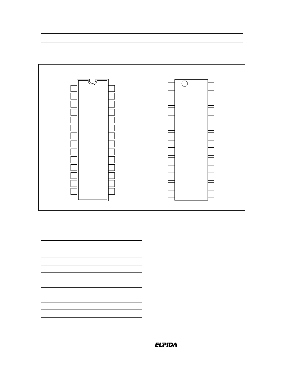
Pin Arrangement
28
27
26
25
24
23
22
21
20
19
18
17
16
15
1
2
3
4
5
6
7
8
9
10
11
12
13
14
V
CC
I/O0
I/O1
I/O2
I/O3
WE
RAS
NC
A10
A0
A1
A2
A3
V
CC
V
I/O7
I/O6
I/O5
I/O4
CAS
OE
A9
A8
A7
A6
A5
A4
V
SS
SS
(Top view)
28
27
26
25
24
23
22
21
20
19
18
17
16
15
1
2
3
4
5
6
7
8
9
10
11
12
13
14
V
CC
I/O0
I/O1
I/O2
I/O3
WE
RAS
NC
A10
A0
A1
A2
A3
V
CC
V
I/O7
I/O6
I/O5
I/O4
CAS
OE
A9
A8
A7
A6
A5
A4
V
SS
SS
HM5117805TS/LTS Series
(Top view)
HM5117805S/LS Series
HM5117805TT/LTT Series
HM5117805J/LJ Series
Pin Description
Pin name
Function
A0 to A10
Address input
-- Row/Refresh address
-- Column address
A0 to A10
A0 to A9
I/O0 to I/O7
Data input/Data output
RAS
Row address strobe
CAS
Column address strobe
WE
Read/Write enable
OE
Output enable
V
CC
Power supply
V
SS
Ground
NC
No connection

EOL Product
HM5117805 Series
Data Sheet E0156H10
4
Block Diagram
∑
∑
∑
∑
∑
∑
A0
A1
to
A9
Timing and control
Column
address
buffers
Row
address
buffers
I/O buffers
I/O0
to
I/O7
RAS
CAS
WE
OE
Column decoder
Row decoder
2M array
2M array
2M array
2M array
2M array
2M array
2M array
2M array
A10
EOL Product
HM5117805 Series
Data Sheet E0156H10
5
Absolute Maximum Ratings
Parameter
Symbol
Value
Unit
Voltage on any pin relative to V
SS
V
T
≠1.0 to +7.0
V
Supply voltage relative to V
SS
V
CC
≠1.0 to +7.0
V
Short circuit output current
Iout
50
mA
Power dissipation
P
T
1.0
W
Operating temperature
Topr
0 to +70
∞C
Storage temperature
Tstg
≠55 to +125
∞C
Recommended DC Operating Conditions (Ta = 0 to +70∞C)
Parameter
Symbol
Min
Typ
Max
Unit
Note
Supply voltage
V
CC
4.5
5.0
5.5
V
1
Input high voltage
V
IH
2.4
--
6.5
V
1
Input low voltage
V
IL
≠1.0
--
0.8
V
1
Note:
1. All voltage referred to V
SS
.

EOL Product
HM5117805 Series
Data Sheet E0156H10
6
DC Characteristics (Ta = 0 to +70∞C, V
CC
= 5 V ± 10%, V
SS
= 0 V)
HM5117805
-5
-6
-7
Parameter
Symbol
Min Max Min Max Min Max Unit
Test conditions
Operating current*
1,
*
2
I
CC1
--
110 --
100 --
90
mA
t
RC
= min
Standby current
I
CC2
--
2
--
2
--
2
mA
TTL interface
RAS
,
CAS
= V
IH
Dout = High-Z
--
1
--
1
--
1
mA
CMOS interface
RAS
,
CAS
V
CC
≠ 0.2 V
Dout = High-Z
Standby current
(L-version)
I
CC2
--
150 --
150 --
150 µA
CMOS interface
RAS
,
CAS
V
CC
≠ 0.2 V
Dout = High-Z
RAS
-only refresh current*
2
I
CC3
--
110 --
100 --
90
mA
t
RC
= min
Standby current*
1
I
CC5
--
5
--
5
--
5
mA
RAS
= V
IH
CAS
= V
IL
Dout = enable
CAS
-before-
RAS
refresh
current
I
CC6
--
110 --
100 --
90
mA
t
RC
= min
EDO page mode
current*
1,
*
3
I
CC7
--
100 --
90
--
85
mA
t
HPC
= min
Battery backup current*
4
(Standby with CBR refresh)
(L-version)
I
CC10
--
500 --
500 --
500 µA
CMOS interface
Dout = High-Z
CBR refresh:
t
RC
= 62.5 µs
t
RAS
0.3 µs
Self refresh mode current
(L-version)
I
CC11
--
300 --
300 --
300 µA
CMOS interface
RAS
,
CAS
0.2V
Dout = High-Z
Input leakage current
I
LI
≠10 10
≠10 10
≠10 10
µA
0 V
Vin
7 V
Output leakage current
I
LO
≠10 10
≠10 10
≠10 10
µA
0 V
Vout
7 V
Dout = disable
Output high voltage
V
OH
2.4
V
CC
2.4
V
CC
2.4
V
CC
V
High Iout = ≠2 mA
Output low voltage
V
OL
0
0.4
0
0.4
0
0.4
V
Low Iout = 2 mA
Notes: 1. I
CC
depends on output load condition when the device is selected. I
CC
max is specified at the output
open condition.
2. Address can be changed once or less while
RAS
= V
IL
.
3. Address can be changed once or less while
CAS
= V
IH
.
4.
CAS
= L (
0.2 V) while
RAS
= L (
0.2 V).

EOL Product
HM5117805 Series
Data Sheet E0156H10
7
Capacitance (Ta = 25∞C, V
CC
= 5 V ± 10%)
Parameter
Symbol
Typ
Max
Unit
Notes
Input capacitance (Address)
C
I1
--
5
pF
1
Input capacitance (Clocks)
C
I2
--
7
pF
1
Output capacitance (Data-in, Data-out)
C
I/O
--
7
pF
1, 2
Notes: 1. Capacitance measured with Boonton Meter or effective capacitance measuring method.
2.
CAS
= V
IH
to disable Dout.
AC Characteristics (Ta = 0 to +70∞C, V
CC
= 5 V ±10%, V
SS
= 0 V)
*1, *2, *18
Test Conditions
∑
Input rise and fall time: 2 ns
∑
Input levels: V
IL
= 0 V, V
IH
= 3 V
∑
Input timing reference levels: 0.8 V, 2.4 V
∑
Output timing reference levels: 0.8 V, 2.0 V
∑
Output load: 1 TTL gate + C
L
(100 pF) (Including scope and jig)

EOL Product
HM5117805 Series
Data Sheet E0156H10
8
Read, Write, Read-Modify-Write and Refresh Cycles (Common parameters)
HM5117805
-5
-6
-7
Parameter
Symbol
Min
Max
Min
Max
Min
Max
Unit
Notes
Random read or write cycle time
t
RC
84
--
104
--
124
--
ns
RAS
precharge time
t
RP
30
--
40
--
50
--
ns
CAS
precharge time
t
CP
7
--
10
--
13
--
ns
RAS
pulse width
t
RAS
50
10000 60
10000 70
10000 ns
CAS
pulse width
t
CAS
7
10000 10
10000 13
10000 ns
Row address setup time
t
ASR
0
--
0
--
0
--
ns
Row address hold time
t
RAH
7
--
10
--
10
--
ns
Column address setup time
t
ASC
0
--
0
--
0
--
ns
Column address hold time
t
CAH
7
--
10
--
13
--
ns
RAS
to
CAS
delay time
t
RCD
11
37
14
45
14
52
ns
3
RAS
to column address delay time t
RAD
9
25
12
30
12
35
ns
4
RAS
hold time
t
RSH
10
--
13
--
13
--
ns
CAS
hold time
t
CSH
35
--
40
--
45
--
ns
CAS
to
RAS
precharge time
t
CRP
5
--
5
--
5
--
ns
OE
to Din delay time
t
OED
13
--
15
--
18
--
ns
5
OE
delay time from Din
t
DZO
0
--
0
--
0
--
ns
6
CAS
delay time from Din
t
DZC
0
--
0
--
0
--
ns
6
Transition time (rise and fall)
t
T
2
50
2
50
2
50
ns
7

EOL Product
HM5117805 Series
Data Sheet E0156H10
9
Read Cycle
HM5117805
-5
-6
-7
Parameter
Symbol
Min
Max
Min
Max
Min
Max
Unit
Notes
Access time from
RAS
t
RAC
--
50
--
60
--
70
ns
8, 9
Access time from
CAS
t
CAC
--
13
--
15
--
18
ns
9, 10, 17
Access time from address
t
AA
--
25
--
30
--
35
ns
9, 11, 17
Access time from
OE
t
OEA
--
13
--
15
--
18
ns
9
Read command setup time
t
RCS
0
--
0
--
0
--
ns
Read command hold time to
CAS
t
RCH
0
--
0
--
0
--
ns
12
Read command hold time from
RAS
t
RCHR
50
--
60
--
70
--
ns
Read command hold time to
RAS
t
RRH
0
--
0
--
0
--
ns
12
Column address to
RAS
lead time
t
RAL
25
--
30
--
35
--
ns
Column address to
CAS
lead time
t
CAL
15
--
18
--
23
--
ns
CAS
to output in low-Z
t
CLZ
0
--
0
--
0
--
ns
Output data hold time
t
OH
3
--
3
--
3
--
ns
20
Output data hold time from
OE
t
OHO
3
--
3
--
3
--
ns
Output buffer turn-off time
t
OFF
--
13
--
15
--
15
ns
13, 20
Output buffer turn-off to
OE
t
OEZ
--
13
--
15
--
15
ns
13
CAS
to Din delay time
t
CDD
13
--
15
--
18
--
ns
5
Output data hold time from
RAS
t
OHR
3
--
3
--
3
--
ns
20
Output buffer turn-off to
RAS
t
OFR
--
13
--
15
--
15
ns
20
Output buffer turn-off to
WE
t
WEZ
--
13
--
15
--
15
ns
WE
to Din delay time
t
WED
13
--
15
--
18
--
ns
RAS
to Din delay time
t
RDD
13
--
15
--
18
--
ns
RAS
next
CAS
delay time
t
RNCD
50
--
60
--
70
--
ns

EOL Product
HM5117805 Series
Data Sheet E0156H10
10
Write Cycle
HM5117805
-5
-6
-7
Parameter
Symbol
Min
Max
Min
Max
Min
Max
Unit
Notes
Write command setup time
t
WCS
0
--
0
--
0
--
ns
14
Write command hold time
t
WCH
7
--
10
--
13
--
ns
Write command pulse width
t
WP
7
--
10
--
10
--
ns
Write command to
RAS
lead time
t
RWL
7
--
10
--
13
--
ns
Write command to
CAS
lead time
t
CWL
7
--
10
--
13
--
ns
Data-in setup time
t
DS
0
--
0
--
0
--
ns
15
Data-in hold time
t
DH
7
--
10
--
13
--
ns
15
Read-Modify-Write Cycle
HM5117805
-5
-6
-7
Parameter
Symbol
Min
Max
Min
Max
Min
Max
Unit
Notes
Read-modify-write cycle time
t
RWC
111
--
135
--
161
--
ns
RAS
to
WE
delay time
t
RWD
67
--
79
--
92
--
ns
14
CAS
to
WE
delay time
t
CWD
30
--
34
--
40
--
ns
14
Column address to
WE
delay time
t
AWD
42
--
49
--
57
--
ns
14
OE
hold time from
WE
t
OEH
13
--
15
--
18
--
ns
Refresh Cycle
HM5117805
-5
-6
-7
Parameter
Symbol
Min
Max
Min
Max
Min
Max
Unit
Notes
CAS
setup time (CBR refresh cycle) t
CSR
5
--
5
--
5
--
ns
CAS
hold time (CBR refresh cycle)
t
CHR
7
--
10
--
10
--
ns
WE
setup time (CBR refresh cycle)
t
WRP
0
--
0
--
0
--
ns
WE
hold time (CBR refresh cycle)
t
WRH
7
--
10
--
10
--
ns
RAS
precharge to
CAS
hold time
t
RPC
5
--
5
--
5
--
ns

EOL Product
HM5117805 Series
Data Sheet E0156H10
11
EDO Page Mode Cycle
HM5117805
-5
-6
-7
Parameter
Symbol
Min Max
Min Max
Min Max
Unit
Notes
EDO page mode cycle time
t
HPC
20
--
25
--
30
--
ns
19
EDO page mode
RAS
pulse width
t
RASP
--
100000 --
100000 --
100000 ns
16
Access time from
CAS
precharge
t
CPA
--
28
--
35
--
40
ns
9, 17
RAS
hold time from
CAS
precharge t
CPRH
28
--
35
--
40
--
ns
Output data hold time from
CAS
low t
DOH
3
--
3
--
3
--
ns
9, 17
CAS
hold time referred
OE
t
COL
7
--
10
--
13
--
ns
CAS
to
OE
setup time
t
COP
5
--
5
--
5
--
ns
Read command hold time from
CAS
precharge
t
RCHC
28
--
35
--
40
--
ns
EDO Page Mode Read-Modify-Write Cycle
HM5117805
-5
-6
-7
Parameter
Symbol
Min
Max
Min
Max
Min
Max
Unit
Notes
EDO page mode read- modify-write
cycle time
t
HPRWC
57
--
68
--
79
ns
WE
delay time from
CAS
precharge t
CPW
45
--
54
--
62
ns
14
Refresh
Parameter
Symbol
Max
Unit
Note
Refresh period
t
REF
32
ms
2048 cycles
Refresh period (L-version)
t
REF
128
ms
2048 cycles
EOL Product
HM5117805 Series
Data Sheet E0156H10
12
Self Refresh Mode (L-version)
HM5117805L
-5
-6
-7
Parameter
Symbol
Min
Max
Min
Max
Min
Max
Unit
Notes
RAS
pulse width (self refresh)
t
RASS
100
--
100
--
100
--
µs
RAS
precharge time (self refresh)
t
RPS
90
--
110
--
130
--
ns
CAS
hold time (self refresh)
t
CHS
≠50
--
≠50
--
≠50
--
ns
Notes: 1. AC measurements assume t
T
= 2 ns.
2. An initial pause of 200 µs is required after power up followed by a minimum of eight initialization
cycles (any combination of cycles containing
RAS
-only refresh or
CAS
-before-
RAS
refresh). If the
internal refresh counter is used, a minimum of eight
CAS
-before-
RAS
refresh cycles are required.
3. Operation with the t
RCD
(max) limit insures that t
RAC
(max) can be met, t
RCD
(max) is specified as a
reference point only; if t
RCD
is greater than the specified t
RCD
(max) limit, then access time is
controlled exclusively by t
CAC
.
4. Operation with the t
RAD
(max) limit insures that t
RAC
(max) can be met, t
RAD
(max) is specified as a
reference point only; if t
RAD
is greater than the specified t
RAD
(max) limit, then access time is
controlled exclusively by t
AA
.
5. Either t
OED
or t
CDD
must be satisfied.
6. Either t
DZO
or t
DZC
must be satisfied.
7. V
IH
(min) and V
IL
(max) are reference levels for measuring timing of input signals. Also, transition
times are measured between V
IH
(min) and V
IL
(max).
8. Assumes that t
RCD
t
RCD
(max) and t
RAD
t
RAD
(max). If t
RCD
or t
RAD
is greater than the maximum
recommended value shown in this table, t
RAC
exceeds the value shown.
9. Measured with a load circuit equivalent to 1 TTL loads and 100 pF.
10. Assumes that t
RCD
t
RCD
(max) and t
RAD
t
RAD
(max).
11. Assumes that t
RCD
t
RCD
(max) and t
RAD
t
RAD
(max).
12. Either t
RCH
or t
RRH
must be satisfied for a read cycles.
13. t
OFF
(max) and t
OEZ
(max) define the time at which the outputs achieve the open circuit condition and
are not referred to output voltage levels.
14. t
WCS
, t
RWD
, t
CWD
, t
AWD
and t
CPW
are not restrictive operating parameters. They are included in the data
sheet as electrical characteristics only; if t
WCS
t
WCS
(min), the cycle is an early write cycle and the
data out pin will remain open circuit (high impedance) throughout the entire cycle; if t
RWD
t
RWD
(min),
t
CWD
t
CWD
(min), and t
AWD
t
AWD
(min), or t
CWD
t
CWD
(min), t
AWD
t
AWD
(min) and t
CPW
t
CPW
(min), the
cycle is a read-modify-write and the data output will contain data read from the selected cell; if
neither of the above sets of conditions is satisfied, the condition of the data out (at access time) is
indeterminate.
15. These parameters are referred to
CAS
leading edge in early write cycles and to
WE
leading edge
in delayed write or read-modify-write cycles.
16. t
RASP
defines
RAS
pulse width in EDO page mode cycles.
17. Access time is determined by the longest among t
AA
, t
CAC
and t
CPA
.
18. In delayed write or read-modify-write cycles,
OE
must disable output buffer prior to applying data
to the device.
19. t
HPC
(min) can be achieved during a series of EDO page mode write cycles or EDO page mode read
cycles. If both write and read operation are mixed in a EDO page mode
RAS
cycle (EDO page
mode mix cycle (1), (2)), minimum value of
CAS
cycle (t
CAS
+ t
CP
+ 2 t
T
) becomes greater than the
specified t
HPC
(min) value.The value of
CAS
cycle time of mixed EDO page mode is shown in EDO
page mode mix cycle (1) and (2).

EOL Product
HM5117805 Series
Data Sheet E0156H10
13
20. Data output turns off and becomes high impedance from later rising edge of
RAS
and
CAS
. Hold
time and turn off time are specified by the timing specifications of later rising edge of
RAS
and
CAS
between t
OHR
and t
OH
and between t
OFR
and t
OFF
.
21. Please do not use t
RASS
timing, 10 µs
t
RASS
100 µs. During this period, the device is in transition
state from normal operation mode to self refresh mode. If t
RASS
100 µs, then
RAS
precharge time
should use t
RPS
instead of t
RP
.
22. If you use
RAS
only refresh or CBR burst refresh mode in normal read/write cycles, 2048 cycles of
distributed CBR refresh with 15.6 µs interval should be executed within 32 ms immediately after
exiting from and before entering into the self refresh mode.
23. If you use distributed CBR refresh mode with 15.6 µs interval in normal read/write cycle, CBR
refresh should be executed within 15.6 µs immediately after exiting from and before entering into
self refresh mode.
24. Repetitive self refresh mode without refreshing all memory is not allowed. Once you exit from self
fresh mode, all memory cells need to be refreshed before re-entering the self refresh mode again.
25. XXX: H or L (H: V
IH
(min)
V
IN
V
IH
(max), L: V
IL
(min)
V
IN
V
IL
(max))
///////: Invalid Dout
When the address, clock and input pins are not described on timing waveforms, their pins must be
applied V
IH
or V
IL
.
EOL Product
HM5117805 Series
Data Sheet E0156H10
14
Timing Waveforms
*25
Read Cycle
RAS
Address
WE
Dout
OE
Din
t
RC
t
RAS
t
RP
t
CSH
t
CRP
t
RCD
t
RSH
t
CAS
t
T
t
RAD
t
RAL
t
CAL
t
ASC
t
CAH
t
ASR
Row
Column
t
RAH
t
RCS
t
RCH
t
RRH
t
CDD
t
DZC
High-Z
Dout
t
DZO
t
OED
t
RAC
t
OEA
t
AA
t
CAC
t
CLZ
t
OH
t
OFF
t
OHO
t
OEZ
CAS
t
RDD
t
WED
t
OFR
t
OHR
t
WEZ
t
RCHR
EOL Product
HM5117805 Series
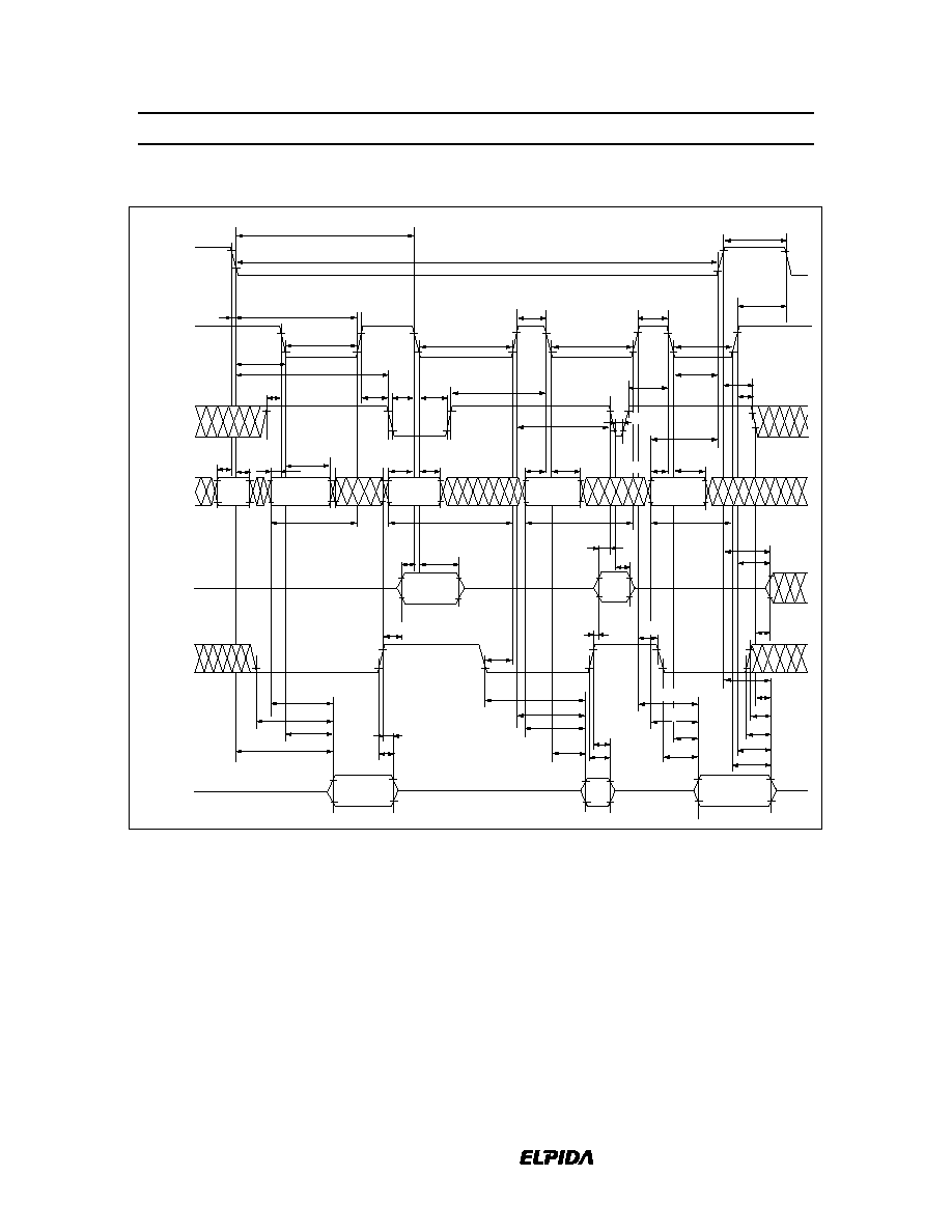
Data Sheet E0156H10
15
Early Write Cycle
RAS
Address
WE
Din
Dout
t
RC
*
t
RAS
t
RP
t
CRP
t
CSH
t
RCD
t
RSH
t
CAS
t
T
t
ASR
t
RAH
t
ASC
t
CAH
Column
Row
t
WCS
t
WCH
t
DS
t
DH
Din
t
WCS
WCS
(min)
High-Z*
t
CAS
EOL Product
HM5117805 Series
Data Sheet E0156H10
16
Delayed Write Cycle
*18
Address
CAS
RAS
WE
Din
OE
Dout
t
RC
t
RAS
t
RP
t
CSH
t
RCD
t
RSH
t
CAS
t
CRP
t
T
Column
Row
t
ASR
t
RAH
t
ASC
t
CAH
t
RCS
t
CWL
t
RWL
t
WP
t
DZC
t
DS
t
DH
t
DZO
t
OED
t
OEH
t
CLZ
t
OEZ
High-Z
Din
High-Z
Invalid Dout

EOL Product
HM5117805 Series
Data Sheet E0156H10
17
Read-Modify-Write Cycle
*18
!
"
Address
RAS
Din
Dout
OE
WE
t
RWC
t
RAS
t
RP
t
CRP
t
CAS
t
RCD
t
T
t
RAD
t
ASR
t
RAH
t
ASC
t
CAH
Column
Row
t
RCS
t
CWD
t
CWL
t
AWD
t
RWD
t
RWL
t
WP
t
DZC
t
DH
t
DS
Din
High-Z
t
DZO
t
OED
t
OEH
t
OEA
t
CAC
t
AA
t
RAC
t
OHO
t
OEZ
t
CLZ
Dout
High-Z
CAS

EOL Product
HM5117805 Series
Data Sheet E0156H10
18
RAS-Only Refresh Cycle
!
RAS
CAS
Address
Dout
High-Z
Row
t
RC
t
RP
t
RAS
t
T
t
CRP
t
RPC
t
CRP
t
ASR
t
RAH
t
OFF
t
OFR

EOL Product
HM5117805 Series
Data Sheet E0156H10
19
CAS-Before-RAS Refresh Cycle
,
RAS
CAS
WE
Dout
Address
t
RC
t
RP
t
RAS
t
RPC
t
CSR
t
CHR
t
RPC
t
CRP
t
CP
t
WRH
t
WRP
t
CP
t
T
t
OFF
t
OFR
High-Z
t
RP

EOL Product
HM5117805 Series
Data Sheet E0156H10
20
Hidden Refresh Cycle
"
0
Din
OE
Dout
WE
Address
RAS
t
RC
t
RC
t
RC
t
RP
t
RAS
t
RP
t
RAS
t
RP
t
RAS
t
T
t
RCD
t
RSH
t
CHR
t
CRP
t
RAD
t
RAL
t
CAH
t
ASC
t
RAH
t
ASR
t
t
CDD
t
DZC
DZO
t
OED
t
OEZ
t
OHO
t
OFF
t
OH
t
CAC
t
AA
t
RAC
t
CLZ
t
Dout
Column
Row
OEA
t
High-Z
t
RCH
t
RRH
CAS
t
WED
t
RDD
WEZ
t
OFR
t
OHR
t
RCS
t
WRH
t
RRH
t
WRP
�
t
WRH
t
WRP
EOL Product
HM5117805 Series
Data Sheet E0156H10
21
EDO Page Mode Read Cycle
Din
OE
Dout
WE
Address
RAS
CAS
t
CP
t
CP
t
CP
t
T
t
RCH
t
RRH
t
DZC
t
CDD
t
RDD
High-Z
t
OFR
t
OEZ
t
OHO
t
OFF
t
OH
t
OHR
t
t
COL
t
t
CPA
t
AA
t
CAC
t
CAC
t
OEA
t
AA
t
RAC
t
AA
t
CAC
t
CPA
t
t
OEZ
t
OEA
t
OEZ
t
AA
t
CAC
t
t
RASP
COP
t
RP
t
CAS
t
CAS
t
CAS
t
CAL
t
CSH
t
HPC
t
HPC
CRP
t
t
ASR
t
RAH
Column 1
Column 2
Column 3
Column 4
t
t
CAH
t
ASC
t
CAH
t
CAH
t
ASC
t
CAH
t
ASC
t
WED
t
RAL
Row
Dout 2
Dout 2
Dout 4
Dout 1
t
CAS
t
RCS
t
t
RCS
Dout 3
t
OHO
t
t
CPRH
t
HPC
t
OEA
t
WEZ
DZO
t
OED
t
RNCD
OHO
DOH
RCH
t
RCHR
t
CAL
t
CAL
t
CAL
t
RSH
t
RCHC
CPA
ASC
EOL Product
HM5117805 Series
Data Sheet E0156H10
22
EDO Page Mode Early Write Cycle
* t
WCS
WCS
(min)
RAS
Address
WE
Din
Dout
t
RASP
t
RP
t
T
t
CSH
t
HPC
t
RSH
t
CRP
t
CAS
t
CP
t
CAS
t
CP
t
CAS
t
RCD
t
ASR
t
RAH
t
ASC
t
CAH
t
ASC
t
CAH
t
ASC
t
CAH
t
WCH
t
WCS
t
WCH
t
WCS
t
WCH
t
WCS
t
DH
t
DS
t
DH
t
DS
t
DH
t
DS
Din 1
Din 2
Din N
High-Z*
t
Row
Column 1
Column 2
Column N
CAS

EOL Product
HM5117805 Series
Data Sheet E0156H10
23
EDO Page Mode Delayed Write Cycle
*18
0
"
WE
Din
OE
Dout
Address
RAS
t
RASP
t
RP
t
CRP
t
RSH
t
CAS
t
HPC
t
CAS
t
CAS
t
CSH
t
RCD
t
T
t
CP
t
CP
t
ASC
t
CAH
t
ASC
t
CAH
t
ASC
t
CAH
t
RAD
t
ASR
t
RAH
t
RCS
t
RCS
t
RCS
t
RWL
t
CWL
t
CWL
t
CWL
t
WP
t
WP
t
WP
t
DZC
t
DS
t
DZC
t
DS
t
DS
t
DZC
t
DH
t
DH
t
DH
t
DZO
t
OED
t
DZO
t
OED
t
DZO
t
OED
t
OEH
t
OEH
t
OEH
t
OEZ
t
CLZ
t
CLZ
t
OEZ
t
CLZ
t
OEZ
Invalid Dout
Invalid Dout
Invalid Dout
Din
1
Din
2
Din
N
Column N
Column 2
Column 1
Row
High-Z
CAS

EOL Product
HM5117805 Series
Data Sheet E0156H10
24
EDO Page Mode Read-Modify-Write Cycle
*18
*
WE
Din
OE
Dout
Address
RAS
t
RASP
t
CRP
t
CP
t
HPRWC
t
T
t
RCD
t
CAS
t
CP
t
CAS
t
CAS
t
RAD
t
ASR
t
ASC
t
ASC
t
ASC
t
RAH
t
CAH
t
CAH
t
CAH
t
CWL
t
CPW
t
CWL
t
CPW
t
CWL
t
RWD
t
AWD
t
AWD
t
AWD
t
CWD
t
RCS
t
CWD
t
RCS
t
CWD
t
RCS
t
WP
t
WP
t
WP
t
DS
t
DZC
t
DS
t
DZC
t
DS
t
DZC
t
DH
t
DH
t
DH
t
DZO
t
DZO
t
DZO
t
OEH
t
OEH
t
OEH
t
AA
t
RAC
t
OEZ
t
CLZ
Dout N
Dout 2
Dout 1
Din
1
Din
2
Din
N
Column N
Column 2
Column 1
t
RP
Row
t
RWL
t
OHO
t
OEA
t
CAC
t
OEZ
t
CLZ
t
OHO
t
OEA
t
CAC
t
CPA
t
OEZ
t
CLZ
t
OHO
t
OEA
t
CAC
t
CPA
High-Z
t
OED
t
OED
t
OED
AA
t
AA
t
t
RSH
CAS

EOL Product
HM5117805 Series
Data Sheet E0156H10
25
EDO Page Mode Mix Cycle (1)
Din
OE
Dout
WE
Address
RAS
CAS
t
CP
t
CP
t
CP
t
T
t
RCH
t
RRH
t
CDD
t
RDD
High-Z
t
OFR
t
OEZ
t
OHO
t
OFF
t
OH
t
CPA
t
AA
t
CAC
t
AA
t
CAC
t
CPA
t
OEZ
t
AA
t
OEA
t
t
RASP
t
RP
t
CAS
t
CAS
t
CAS
CRP
t
t
ASR
t
RAH
Column 1
Column 2
Column 3
Column 4
t
ASC
t
CAH
t
ASC
t
CAH
t
CAH
t
CAH
t
RAL
t
CAL
Row
Dout 2
Dout 4
CPA
t
CAS
t
WCS
Dout 3
t
t
t
WP
t
WCH
t
WED
t
WEZ
t
DS
t
DH
t
DS
t
DH
Din 3
Din 1
t
OEA
t
OED
t
CAC
t
ASC
t
CPW
t
AWD
OHO
t
CAL
t
CAL
t
CAL
t
RCS
t
RCS
t
CSH
t
RCD
t
RSH
DOH
ASC
t
EOL Product
HM5117805 Series
Data Sheet E0156H10
26
EDO Page Mode Mix Cycle (2)
Din
OE
Dout
WE
Address
RAS
CAS
t
CP
t
RNCD
t
CP
t
T
t
RCH
t
RRH
t
CDD
t
RDD
High-Z
t
OFR
t
OEZ
t
OHO
t
OFF
t
OH
t
CPA
t
AA
t
CAC
t
AA
t
CAC
t
OEZ
t
t
OEA
t
t
RASP
t
RP
t
CAS
t
CAS
t
CAS
t
CSH
CRP
t
t
ASR
t
RAH
Column 1
Column 2
Column 3
Column 4
t
ASC
t
CAH
t
ASC
t
CAH
t
CAH
t
ASC
t
CAH
t
RAL
t
RCS
Row
Dout 1
Dout 4
CPA
t
CAS
Dout 3
t
OHO
t
WED
t
WEZ
t
DS
t
DH
t
DS
t
Din 3
Din 2
t
OEA
t
t
CAC
t
CPW
t
RCH
t
RCS
t
WCH
t
RAC
t
OED
t
COL
t
OEA
t
OHO
t
OEZ
t
DH
OED
t
RCS
t
CAL
t
CAL
t
CAL
t
CAL
t
RCD
t
RCHR
t
WCS
t
RSH
t
WP
t
ASC
AA
COP
EOL Product
HM5117805 Series
Data Sheet E0156H10
27
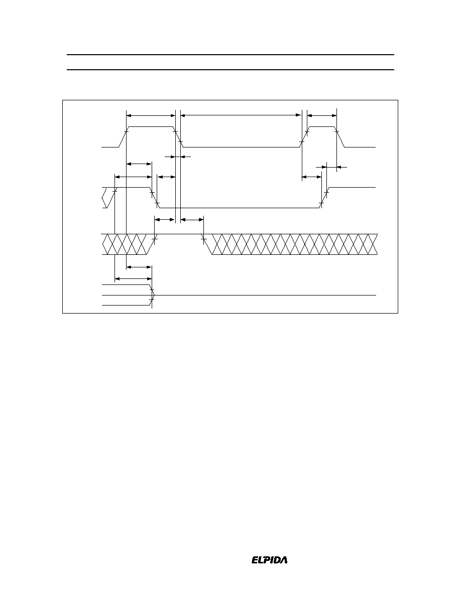
Self Refresh Cycle (L-version)
*21, 22, 23, 24
$
&
+
,
,
,
RAS
Dout
t
RP
t
RASS
t
RPS
t
RPC
t
T
t
CP
t
CSR
t
CHS
t
CRP
t
OFF
t
OFR
High-Z
CAS
WRP
t
WRH
t
WE

EOL Product
HM5117805 Series
Data Sheet E0156H10
28
Package Dimensions
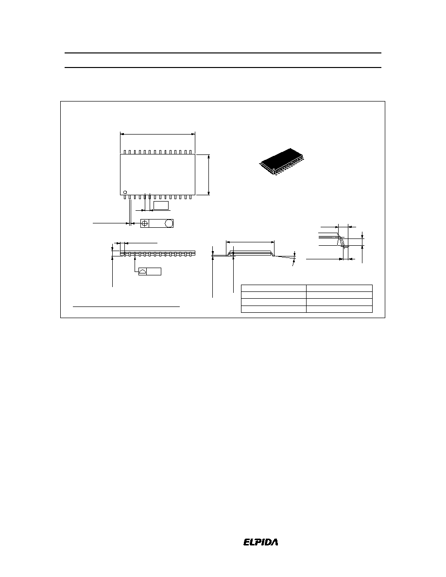
HM5117805J/LJ Series (CP-28DA)
9.40
±
0.25
1
14
0.43
±
0.10
3.50
±
0.26
15
28
18.54 Max
18.17
0.74
10.16
±
0.13
11.18
±
0.13
0.10
2.85
±
0.12
1.30 Max
1.27
0.80
+0.25 ≠0.17
Hitachi Code
JEDEC
EIAJ
Weight (reference value)
CP-28DA
Conforms
Conforms
1.16 g
0.41
±
0.08
Unit: mm
Dimension including the plating thickness
Base material dimension

EOL Product
HM5117805 Series
Data Sheet E0156H10
29
HM5117805S/LS Series (CP-28DNA)
0.43
±
0.10
3.50
±
0.26
1.165 Max
0.10
1.27
Hitachi Code
JEDEC
EIAJ
Weight (reference value)
CP-28DNA
--
--
0.95 g
0.41
±
0.08
Unit: mm
15
28
1
14
6.79
±
0.18
+ 0.25
≠ 0.36
2.45
0.74
18.84 Max
18.41
7.62
±
0.12
8.51
±
0.12
0.90
±
0.26
Dimension including the plating thickness
Base material dimension

EOL Product
HM5117805 Series
Data Sheet E0156H10
30
HM5117805TT/LTT Series (TTP-28DA)
1.27
0.21
M
0.42
±
0.08
0.10
10.16
18.41
18.81 Max
15
14
28
1
1.20 Max
0
∞
≠ 5
∞
0.13
±
0.05
11.76
±
0.20
0.50
±
0.10
1.15 Max
0.145
±
0.05
0.68
0.80
Hitachi Code
JEDEC
EIAJ
Weight (reference value)
TTP-28DA
Conforms
--
0.43 g
0.40
±
0.06
0.125
±
0.04
Unit: mm
Dimension including the plating thickness
Base material dimension
EOL Product
HM5117805 Series
Data Sheet E0156H10
31
HM5117805TS/LTS Series (TTP-28DB)
Hitachi Code
JEDEC
EIAJ
Weight (reference value)
TTP-28DB
--
--
0.35 g
18.41
18.81 Max
1
14
28
15
1.27
0.21
0.42
±
0.08
1.20 Max
0.10
7.62
9.22
±
0.2
0.13
±
0.05
0
∞
≠ 5
∞
M
1.15 Max
0.50
±
0.10
0.63
0.145
±
0.05
0.40
±
0.06
0.125
±
0.04
0.80
Unit: mm
Dimension including the plating thickness
Base material dimension

EOL Product
HM5117805 Series
Data Sheet E0156H10
32
Cautions
1. Elpida Memory, Inc. neither warrants nor grants licenses of any rights of Elpida Memory, Inc.'s or any
third party's patent, copyright, trademark, or other intellectual property rights for information contained
in this document. Elpida Memory, Inc. bears no responsibility for problems that may arise with third
party's rights, including intellectual property rights, in connection with use of the information contained
in this document.
2. Products and product specifications may be subject to change without notice. Confirm that you have
received the latest product standards or specifications before final design, purchase or use.
3. Elpida Memory, Inc. makes every attempt to ensure that its products are of high quality and reliability.
However, contact Elpida Memory, Inc. before using the product in an application that demands especially
high quality and reliability or where its failure or malfunction may directly threaten human life or cause
risk of bodily injury, such as aerospace, aeronautics, nuclear power, combustion control, transportation,
traffic, safety equipment or medical equipment for life support.
4. Design your application so that the product is used within the ranges guaranteed by Elpida Memory, Inc.
particularly for maximum rating, operating supply voltage range, heat radiation characteristics,
installation conditions and other characteristics. Elpida Memory, Inc. bears no responsibility for failure or
damage when used beyond the guaranteed ranges. Even within the guaranteed ranges, consider normally
foreseeable failure rates or failure modes in semiconductor devices and employ systemic measures such
as fail-safes, so that the equipment incorporating Elpida Memory, Inc. product does not cause bodily
injury, fire or other consequential damage due to operation of the Elpida Memory, Inc. product.
5. This product is not designed to be radiation resistant.
6. No one is permitted to reproduce or duplicate, in any form, the whole or part of this document without
written approval from Elpida Memory, Inc..
7. Contact Elpida Memory, Inc. for any questions regarding this document or Elpida Memory, Inc.
semiconductor products.