Document Outline
- COVER
- ˛ˇ
- ˛ˇ
- ˛ˇ
- Pin Arrangement (5259165B)
- Pin Description (5259165B)
- ˛ˇ
- Pin Description (HM5259805B)
- ˛ˇ
- Pin Description (HM5259405B)
- ˛ˇ
- ˛ˇ
- Block Diagram (HM5259405B)
- ˛ˇ
- ˛ˇ
- ˛ˇ
- ˛ˇ
- ˛ˇ
- ˛ˇ
- ˛ˇ
- ˛ˇ
- ˛ˇ
- DC Characteristics
- ˛ˇ
- ˛ˇ
- ˛ˇ
- ˛ˇ
- ˛ˇ
- ˛ˇ
- Read Cycle/Write Cycle
- ˛ˇ
- Read/Burst Write Cycle
- ˛ˇ
- ˛ˇ
- ˛ˇ
- Power Down Mode
- ˛ˇ
- Package Dimensions
Elpida Memory, Inc. is a joint venture DRAM company of NEC Corporation and Hitachi, Ltd.
HM5259165B-75/A6
HM5259805B-75/A6
HM5259405B-75/A6
512M LVTTL interface SDRAM
133 MHz/100 MHz
8-Mword
◊ 16-bit ◊ 4-bank/16-Mword ◊ 8-bit ◊ 4-bank
/32-Mword
◊ 4-bit ◊ 4-bank
PC/133, PC/100 SDRAM
E0118H10
Ver. 1.0
Apr. 6, 2001
Description
The HM5259165B is a 512-Mbit SDRAM organized as 8388608-word
◊ 16-bit ◊ 4 bank. The HM5259805B
is a 512-Mbit SDRAM organized as 16777216-word
◊ 8-bit ◊ 4 bank. The HM5259405B is a 512-Mbit
SDRAM organized as 33554432-word
◊ 4-bit ◊ 4 bank. All inputs and outputs are referred to the rising edge
of the clock input. It is packaged in standard 54-pin plastic TSOP II.
Features
∑ 3.3 V power supply
∑ Clock frequency: 133 MHz/100 MHz (max)
∑ LVTTL interface
∑ Single pulsed RAS
∑ 4 banks can operate simultaneously and independently
∑ Burst read/write operation and burst read/single write operation capability
∑ Programmable burst length: 1/2/4/8
∑ 2 variations of burst sequence
Sequential (BL = 1/2/4/8)
Interleave (BL = 1/2/4/8)

HM5259165B/HM5259805B/HM5259405B-75/A6
Data Sheet E0118H10
2
∑ Programmable CAS latency: 2/3
∑ Byte control by DQM : DQM (HM5259805B/HM5259405B)
: DQMU/DQML (HM5259165B)
∑ Refresh cycles: 8192 refresh cycles/32 ms
∑ 2 variations of refresh
Auto refresh
Self refresh
Ordering Information
Type No.
Frequency
CAS latency
Package
HM5259165BTD-75*
1
HM5259165BTD-A6
133 MHz
100 MHz
3
2/3
400-mil 54-pin plastic TSOP II (TTP-54DA)
HM5259805BTD-75*
1
HM5259805BTD-A6
133 MHz
100 MHz
3
2/3
HM5259405BTD-75*
1
HM5259405BTD-A6
133 MHz
100 MHz
3
2/3
Notes: 1. 100 MHz operation at
CAS latency = 2

HM5259165B/HM5259805B/HM5259405B-75/A6
Data Sheet E0118H10
3
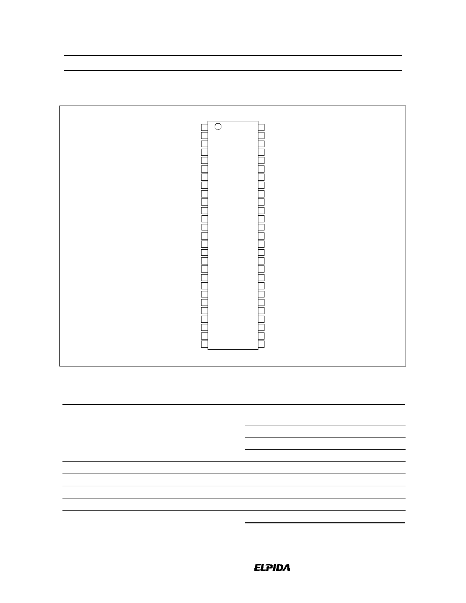
Pin Arrangement (HM5259165B)
1
2
3
4
5
6
7
8
9
10
11
12
13
14
15
16
17
18
19
20
21
22
23
24
25
26
27
54
53
52
51
50
49
48
47
46
45
44
43
42
41
40
39
38
37
36
35
34
33
32
31
30
29
28
V
SS
DQ15
V
SS
Q
DQ14
DQ13
V
CC
Q
DQ12
DQ11
V
SS
Q
DQ10
DQ9
V
CC
Q
DQ8
V
SS
NC
DQMU
CLK
CKE
A12
A11
A9
A8
A7
A6
A5
A4
V
SS
V
CC
DQ0
V
CC
Q
DQ1
DQ2
V
SS
Q
DQ3
DQ4
V
CC
Q
DQ5
DQ6
V
SS
Q
DQ7
V
CC
DQML
WE
CAS
RAS
CS
BA0
BA1
A10
A0
A1
A2
A3
V
CC
54-pin TSOP
(Top view)
Pin Description
Pin name
Function
Pin name
Function
A0 to A12,
BA0, BA1
Address input
WE
Write enable
Row address
A0 to A12
DQMU/DQML
Input/output mask
Column address
A0 to A9
CLK
Clock input
Bank select address BA0/BA1 (BS) CKE
Clock enable
DQ0 to DQ15
Data-input/output
V
CC
Power for internal circuit
CS
Chip select
V
SS
Ground for internal circuit
RAS
Row address strobe command
V
CC
Q
Power for DQ circuit
CAS
Column address strobe command
V
SS
Q
Ground for DQ circuit
NC
No connection
HM5259165B/HM5259805B/HM5259405B-75/A6
Data Sheet E0118H10
4
Pin Arrangement (HM5259805B)
1
2
3
4
5
6
7
8
9
10
11
12
13
14
15
16
17
18
19
20
21
22
23
24
25
26
27
54
53
52
51
50
49
48
47
46
45
44
43
42
41
40
39
38
37
36
35
34
33
32
31
30
29
28
V
SS
DQ7
V
SS
Q
NC
DQ6
V
CC
Q
NC
DQ5
V
SS
Q
NC
DQ4
V
CC
Q
NC
V
SS
NC
DQM
CLK
CKE
A12
A11
A9
A8
A7
A6
A5
A4
V
SS
V
CC
DQ0
V
CC
Q
NC
DQ1
V
SS
Q
NC
DQ2
V
CC
Q
NC
DQ3
V
SS
Q
NC
V
CC
NC
WE
CAS
RAS
CS
BA0
BA1
A10
A0
A1
A2
A3
V
CC
54-pin TSOP
(Top view)
Pin Description
Pin name
Function
Pin name
Function
A0 to A12,
BA0, BA1
Address input
WE
Write enable
Row address
A0 to A12
DQM
Input/output mask
Column address
A0 to A9, A11
CLK
Clock input
Bank select address BA0/BA1 (BS) CKE
Clock enable
DQ0 to DQ7
Data-input/output
V
CC
Power for internal circuit
CS
Chip select
V
SS
Ground for internal circuit
RAS
Row address strobe command
V
CC
Q
Power for DQ circuit
CAS
Column address strobe command
V
SS
Q
Ground for DQ circuit
NC
No connection

HM5259165B/HM5259805B/HM5259405B-75/A6
Data Sheet E0118H10
5
Pin Arrangement (HM5259405B)
1
2
3
4
5
6
7
8
9
10
11
12
13
14
15
16
17
18
19
20
21
22
23
24
25
26
27
54
53
52
51
50
49
48
47
46
45
44
43
42
41
40
39
38
37
36
35
34
33
32
31
30
29
28
V
SS
NC
V
SS
Q
NC
DQ3
V
CC
Q
NC
NC
V
SS
Q
NC
DQ2
V
CC
Q
NC
V
SS
NC
DQM
CLK
CKE
A12
A11
A9
A8
A7
A6
A5
A4
V
SS
V
CC
NC
V
CC
Q
NC
DQ0
V
SS
Q
NC
NC
V
CC
Q
NC
DQ1
V
SS
Q
NC
V
CC
NC
WE
CAS
RAS
CS
BA0
BA1
A10
A0
A1
A2
A3
V
CC
54-pin TSOP
(Top view)
Pin Description
Pin name
Function
Pin name
Function
A0 to A12,
BA0, BA1
Address input
WE
Write enable
Row address
A0 to A12
DQM
Input/output mask
Column address
A0 to A9, A11 A12 CLK
Clock input
Bank select address BA0/BA1 (BS)
CKE
Clock enable
DQ0 to DQ3
Data-input/output
V
CC
Power for internal circuit
CS
Chip select
V
SS
Ground for internal circuit
RAS
Row address strobe command
V
CC
Q
Power for DQ circuit
CAS
Column address strobe command
V
SS
Q
Ground for DQ circuit
NC
No connection

HM5259165B/HM5259805B/HM5259405B-75/A6
Data Sheet E0118H10
6
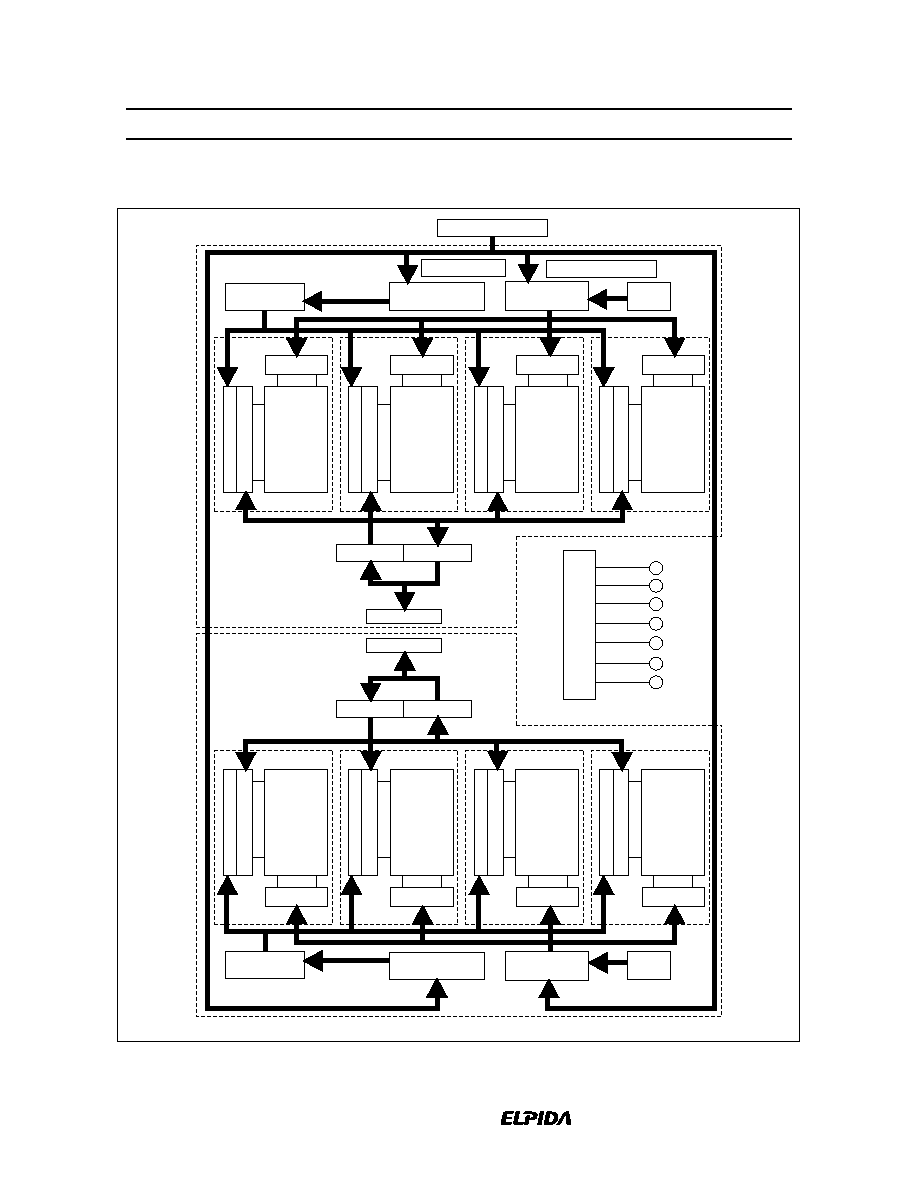
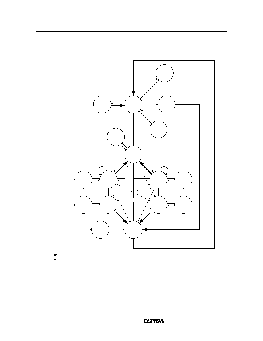
Block Diagram (HM5259165B)
Column address
counter
Column address
buffer
Upper pellet
Lower pellet
Row address
buffer
Refresh
counter
Column address
counter
Column address
buffer
Row address
buffer
Refresh
counter
DQ8 to DQ15
DQ0 to DQ7
Input buffer
Output buffer
Control logic &
timing generator
Row decoder
Sense amplifier & I/O bus
Column decoder
CLK
CKE
CS
RAS
CAS
WE
DQMU
/DQML
A0 to A9
Row decoder
Sense amplifier & I/O bus
Column decoder
Row decoder
Sense amplifier & I/O bus
Column decoder
Row decoder
Row decoder
Row decoder
Row decoder
Row decoder
Sense amplifier & I/O bus
Column decoder
Memory array
Bank0
8192 row
◊ 1024 column
◊ 8 bit
Memory array
Bank1
8192 row
◊ 1024 column
◊ 8 bit
Memory array
Bank2
8192 row
◊ 1024 column
◊ 8 bit
Memory array
Bank3
8192 row
◊ 1024 column
◊ 8 bit
Sense amplifier & I/O bus
Column decoder
Sense amplifier & I/O bus
Column decoder
Sense amplifier & I/O bus
Column decoder
Sense amplifier & I/O bus
Column decoder
Memory array
Bank0
8192 row
◊ 1024 column
◊ 8 bit
Memory array
Bank1
8192 row
◊ 1024 column
◊ 8 bit
Memory array
Bank2
8192 row
◊ 1024 column
◊ 8 bit
Memory array
Bank3
8192 row
◊ 1024 column
◊ 8 bit
Input buffer
Output buffer
A0 to A12, BA0, BA1
A0 to A12, BA0, BA1

HM5259165B/HM5259805B/HM5259405B-75/A6
Data Sheet E0118H10
7
Block Diagram (HM5259805B)
Column address
counter
Column address
buffer
Upper pellet
Lower pellet
Row address
buffer
Refresh
counter
Column address
counter
Column address
buffer
Row address
buffer
Refresh
counter
DQ4 to DQ7
DQ0 to DQ3
Input buffer
Output buffer
Control logic &
timing generator
Row decoder
Sense amplifier & I/O bus
Column decoder
CLK
CKE
CS
RAS
CAS
WE
DQM
A0 to A9, A11
Row decoder
Sense amplifier & I/O bus
Column decoder
Row decoder
Sense amplifier & I/O bus
Column decoder
Row decoder
Row decoder
Row decoder
Row decoder
Row decoder
Sense amplifier & I/O bus
Column decoder
Memory array
Bank0
8192 row
◊ 2048 column
◊ 4 bit
Memory array
Bank1
8192 row
◊ 2048 column
◊ 4 bit
Memory array
Bank2
8192 row
◊ 2048 column
◊ 4 bit
Memory array
Bank3
8192 row
◊ 2048 column
◊ 4 bit
Sense amplifier & I/O bus
Column decoder
Sense amplifier & I/O bus
Column decoder
Sense amplifier & I/O bus
Column decoder
Sense amplifier & I/O bus
Column decoder
Memory array
Bank0
8192 row
◊ 2048 column
◊ 4 bit
Memory array
Bank1
8192 row
◊ 2048 column
◊ 4 bit
Memory array
Bank2
8192 row
◊ 2048 column
◊ 4 bit
Memory array
Bank3
8192 row
◊ 2048 column
◊ 4 bit
Input buffer
Output buffer
A0 to A12, BA0, BA1
A0 to A12, BA0, BA1
HM5259165B/HM5259805B/HM5259405B-75/A6
Data Sheet E0118H10
8
Block Diagram (HM5259405B)
Column address
counter
Column address
buffer
Upper pellet
Lower pellet
Row address
buffer
Refresh
counter
Column address
counter
Column address
buffer
Row address
buffer
Refresh
counter
DQ2 to DQ3
DQ0 to DQ1
Input buffer
Output buffer
Control logic &
timing generator
Row decoder
Sense amplifier & I/O bus
Column decoder
CLK
CKE
CS
RAS
CAS
WE
DQM
Row decoder
Sense amplifier & I/O bus
Column decoder
Row decoder
Sense amplifier & I/O bus
Column decoder
Row decoder
Row decoder
Row decoder
Row decoder
Row decoder
Sense amplifier & I/O bus
Column decoder
Memory array
Bank0
8192 row
◊ 4096 column
◊ 2 bit
Memory array
Bank1
8192 row
◊ 4096 column
◊ 2 bit
Memory array
Bank2
8192 row
◊ 4096 column
◊ 2 bit
Memory array
Bank3
8192 row
◊ 4096 column
◊ 2 bit
Sense amplifier & I/O bus
Column decoder
Sense amplifier & I/O bus
Column decoder
Sense amplifier & I/O bus
Column decoder
Sense amplifier & I/O bus
Column decoder
Memory array
Bank0
8192 row
◊ 4096 column
◊ 2 bit
Memory array
Bank1
8192 row
◊ 4096 column
◊ 2 bit
Memory array
Bank2
8192 row
◊ 4096 column
◊ 2 bit
Memory array
Bank3
8192 row
◊ 4096 column
◊ 2 bit
Input buffer
Output buffer
A0 to A12, BA0, BA1
A0 to A12, BA0, BA1
A0 to A9, A11, A12

HM5259165B/HM5259805B/HM5259405B-75/A6
Data Sheet E0118H10
9
Pin Functions
CLK (input pin): CLK is the master clock input to this pin. The other input signals are referred at CLK
rising edge.
CS (input pin): When CS is Low, the command input cycle becomes valid. When CS is High, all inputs are
ignored. However, internal operations (bank active, burst operations, etc.) are held.
RAS, CAS, and WE (input pins): Although these pin names are the same as those of conventional DRAMs,
they function in a different way. These pins define operation commands (read, write, etc.) depending on the
combination of their voltage levels. For details, refer to the command operation section.
A0 to A12 (input pins): Row address (AX0 to AX12) is determined by A0 to A12 level at the bank active
command cycle CLK rising edge. Column address (AY0 to AY9; HM5259165B, AY0 to AY9, AY11;
HM5259805B, AY0 to AY9, AY11, AY12; HM5259405B) is determined by A0 to A8, A9 A11 or A12 (A9;
HM5259165B, A9, A11; HM5259805B, A9, A11, A12; HM5259405B) level at the read or write command
cycle CLK rising edge. And this column address becomes burst access start address. A10 defines the
precharge mode. When A10 = High at the precharge command cycle, all banks are precharged. But when
A10 = Low at the precharge command cycle, only the bank that is selected by BA0/BA1 (BS) is precharged.
For details refer to the command operation section.
BA0/BA1 (input pin): BA0/BA1 are bank select signal (BS). The memory array of the HM5259165B,
HM5259805B, the HM5259405B is divided into bank 0, bank 1, bank 2 and bank 3. HM5259165B contain
8192-row
◊ 1024-column ◊ 16-bit. HM5259805B contain 8192-row ◊ 2048-column ◊ 8-bit. HM5259405B
contain 8192-row
◊ 4096-column ◊ 4-bit. If BA0 is Low and BA1 is Low, bank 0 is selected. If BA0 is Low
and BA1 is High, bank 1 is selected. If BA0 is High and BA1 is Low, bank 2 is selected. If BA0 is High and
BA1 is High, bank 3 is selected.
CKE (input pin): This pin determines whether or not the next CLK is valid. If CKE is High, the next CLK
rising edge is valid. If CKE is Low, the next CLK rising edge is invalid. This pin is used for power-down
mode, clock suspend mode and self refresh mode.
DQM, DQMU/DQML (input pins): DQM, DQMU/DQML controls input/output buffers.
Read operation: If DQM, DQMU/DQML is High, the output buffer becomes High-Z. If the DQM,
DQMU/DQML is Low, the output buffer becomes Low-Z. (The latency of DQM, DQMU/DQML during
reading is 2 clocks.)
Write operation: If DQM, DQMU/DQML is High, the previous data is held (the new data is not written). If
DQM, DQMU/DQML is Low, the data is written. (The latency of DQM, DQMU/DQML during writing is 0
clock.)
DQ0 to DQ15 (DQ pins): Data is input to and output from these pins (DQ0 to DQ15; HM5259165B, DQ0
to DQ7; HM5259805B, DQ0 to DQ3; HM5259405B).
V
CC
and V
CC
Q (power supply pins): 3.3 V is applied. (V
CC
is for the internal circuit and V
CC
Q is for the
output buffer.)
HM5259165B/HM5259805B/HM5259405B-75/A6
Data Sheet E0118H10
10
V
SS
and V
SS
Q (power supply pins): Ground is connected. (V
SS
is for the internal circuit and V
SS
Q is for the
output buffer.)
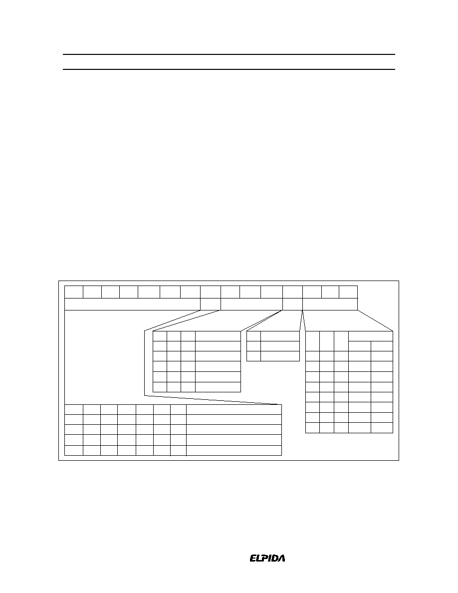
Command Operation
Command Truth Table
The SDRAM recognizes the following commands specified by the
CS, RAS, CAS, WE and address pins.
CKE
Command
Symbol
n - 1 n
CS RAS CAS WE BA0/BA1 A10
A0
to A12
Ignore command
DESL
H
◊
H
◊
◊
◊
◊
◊
◊
No operation
NOP
H
◊
L
H
H
H
◊
◊
◊
Column address and read command READ
H
◊
L
H
L
H
V
L
V
Read with auto-precharge
READ A
H
◊
L
H
L
H
V
H
V
Column address and write command WRIT
H
◊
L
H
L
L
V
L
V
Write with auto-precharge
WRIT A
H
◊
L
H
L
L
V
H
V
Row address strobe and bank active ACTV
H
◊
L
L
H
H
V
V
V
Precharge select bank
PRE
H
◊
L
L
H
L
V
L
◊
Precharge all bank
PALL
H
◊
L
L
H
L
◊
H
◊
Refresh
REF/SELF H
V
L
L
L
H
◊
◊
◊
Mode register set
MRS
H
◊
L
L
L
L
V
V
V
Note:
H: V
IH
. L: V
IL
.
◊: V
IH
or V
IL
. V: Valid address input
Ignore command [DESL]: When this command is set (
CS is High), the SDRAM ignore command input at
the clock. However, the internal status is held.
No operation [NOP]: This command is not an execution command. However, the internal operations
continue.
Column address strobe and read command [READ]: This command starts a read operation. In addition,
the start address of burst read is determined by the column address (AY0 to AY9; HM5259165B, AY0 to
AY9, AY11; HM5259805B, AY0 to AY9, AY11, AY12; HM5259405B) and the bank select address (BS).
After the read operation, the output buffer becomes High-Z.
Read with auto-precharge [READ A]: This command automatically performs a precharge operation after a
burst read with a burst length of 1, 2, 4 or 8.

HM5259165B/HM5259805B/HM5259405B-75/A6
Data Sheet E0118H10
11
Column address strobe and write command [WRIT]: This command starts a write operation. When the
burst write mode is selected, the column address (AY0 to AY9; HM5259165B, AY0 to AY9, AY11;
HM5259805B, AY0 to AY9, AY11, AY12; HM5259405B) and the bank select address (BA0/BA1) become
the burst write start address. When the single write mode is selected, data is only written to the location
specified by the column address (AY0 to AY9; HM5259165B, AY0 to AY9, AY11; HM5259805B, AY0 to
AY9, AY11, AY12; HM5259405B) and the bank select address (BA0/BA1).
Write with auto-precharge [WRIT A]: This command automatically performs a precharge operation after a
burst write with a length of 1, 2, 4 or 8, or after a single write operation.
Row address strobe and bank activate [ACTV]: This command activates the bank that is selected by
BA0/BA1 (BS) and determines the row address (AX0 to AX12). When BA0 and BA1 are Low, bank 0 is
activated. When BA0 is Low and BA1 is High, bank 1 is activated. When BA0 is High and BA1 is Low,
bank 2 is activated. When BA0 and BA1 are High, bank 3 is activated.
Precharge selected bank [PRE]: This command starts precharge operation for the bank selected by
BA0/BA1. If BA0 and BA1 are Low, bank 0 is selected. If BA0 is Low and BA1 is High, bank 1 is selected.
If BA0 is High and BA1 is Low, bank 2 is selected. If BA0 and BA1 are High, bank 3 is selected.
Precharge all banks [PALL]: This command starts a precharge operation for all banks.
Refresh [REF/SELF]: This command starts the refresh operation. There are two types of refresh operation,
the one is auto-refresh, and the other is self-refresh. For details, refer to the CKE truth table section.
Mode register set [MRS]: The SDRAM has a mode register that defines how it operates. The mode register
is specified by the address pins (A0 to BA0 and BA1) at the mode register set cycle. For details, refer to the
mode register configuration. After power on, the contents of the mode register are undefined, execute the
mode register set command to set up the mode register.
HM5259165B/HM5259805B/HM5259405B-75/A6
Data Sheet E0118H10
12
DQM Truth Table (HM5259165B)
CKE
Command
Symbol
n - 1
n
DQMU
DQML
Upper byte (DQ8 to DQ15) write enable/output enable ENBU
H
◊
L
◊
Lower byte (DQ0 to DQ7) write enable/output enable
ENBL
H
◊
◊
L
Upper byte (DQ8 to DQ15) write inhibit/output disable MASKU
H
◊
H
◊
Lower byte (DQ0 to DQ7) write inhibit/output disable
MASKL
H
◊
◊
H
Note:
H: V
IH
. L: V
IL
.
◊: V
IH
or V
IL
.
Write: I
DID
is needed.
Read: I
DOD
is needed.
DQM Truth Table (HM5259805B/HM5259405B)
CKE
Command
Symbol
n - 1
n
DQM
Write enable/output enable
ENB
H
◊
L
Write inhibit/output disable
MASK
H
◊
H
Note:
H: V
IH
. L: V
IL
.
◊: V
IH
or V
IL
.
Write: I
DID
is needed.
Read: I
DOD
is needed.
The SDRAM can mask input/output data by means of DQM, DQMU/DQML.
DQMU masks the upper byte and DQML masks the lower byte. (HM5259165B)
During reading, the output buffer is set to Low-Z by setting DQM, DQMU/DQML to Low, enabling data
output. On the other hand, when DQM, DQMU/DQML is set to High, the output buffer becomes High-Z,
disabling data output.
During writing, data is written by setting DQM, DQMU/DQML to Low. When DQM, DQMU/DQML is set
to High, the previous data is held (the new data is not written). Desired data can be masked during burst read
or burst write by setting DQMU/DQML. For details, refer to the DQM, DQMU/DQML control section of the
SDRAM operating instructions.
HM5259165B/HM5259805B/HM5259405B-75/A6
Data Sheet E0118H10
13
CKE Truth Table
CKE
Current state
Command
n - 1
n
CS
RAS
CAS
WE Address
Active
Clock suspend mode entry
H
L
◊
◊
◊
◊
◊
Any
Clock suspend
L
L
◊
◊
◊
◊
◊
Clock suspend
Clock suspend mode exit
L
H
◊
◊
◊
◊
◊
Idle
Auto-refresh command (REF)
H
H
L
L
L
H
◊
Idle
Self-refresh entry (SELF)
H
L
L
L
L
H
◊
Idle
Power down entry
H
L
L
H
H
H
◊
H
L
H
◊
◊
◊
◊
Self refresh
Self refresh exit (SELFX)
L
H
L
H
H
H
◊
L
H
H
◊
◊
◊
◊
Power down
Power down exit
L
H
L
H
H
H
◊
L
H
H
◊
◊
◊
◊
Note:
H: V
IH
. L: V
IL
.
◊: V
IH
or V
IL
.
Clock suspend mode entry: The SDRAM enters clock suspend mode from active mode by setting CKE to
Low. If command is input in the clock suspend mode entry cycle, the command is valid. The clock suspend
mode changes depending on the current status (1 clock before) as shown below.
ACTIVE clock suspend: This suspend mode ignores inputs after the next clock by internally maintaining
the bank active status.
READ suspend and READ with Auto-precharge suspend: The data being output is held (and continues to
be output).
WRITE suspend and WRIT with Auto-precharge suspend: In this mode, external signals are not
accepted. However, the internal state is held.
Clock suspend: During clock suspend mode, keep the CKE to Low.
Clock suspend mode exit: The SDRAM exits from clock suspend mode by setting CKE to High during the
clock suspend state.
IDLE: In this state, all banks are not selected, and completed precharge operation.
Auto-refresh command [REF]: When this command is input from the IDLE state, the SDRAM starts auto-
refresh operation. (The auto-refresh is the same as the CBR refresh of conventional DRAMs.) During the
auto-refresh operation, refresh address and bank select address are generated inside the SDRAM. For every
auto-refresh cycle, the internal address counter is updated. Accordingly, 8192 times are required to refresh
the entire memory. Before executing the auto-refresh command, all the banks must be in the IDLE state. In
addition, since the precharge for all banks is automatically performed after auto-refresh, no precharge
command is required after auto-refresh.

HM5259165B/HM5259805B/HM5259405B-75/A6
Data Sheet E0118H10
14
Self-refresh entry [SELF]: When this command is input during the IDLE state, the SDRAM starts self-
refresh operation. After the execution of this command, self-refresh continues while CKE is Low. Since self-
refresh is performed internally and automatically, external refresh operations are unnecessary.
Power down mode entry: When this command is executed during the IDLE state, the SDRAM enters power
down mode. In power down mode, power consumption is suppressed by cutting off the initial input circuit.
Self-refresh exit: When this command is executed during self-refresh mode, the SDRAM can exit from self-
refresh mode. After exiting from self-refresh mode, the SDRAM enters the IDLE state.
Power down exit: When this command is executed at the power down mode, the SDRAM can exit from
power down mode. After exiting from power down mode, the SDRAM enters the IDLE state.
Function Truth Table
The following table shows the operations that are performed when each command is issued in each mode of
the SDRAM.
The following table assumes that CKE is high.
Current state
CS
RAS CAS WE
Address
Command
Operation
Precharge
H
◊
◊
◊
◊
DESL
Enter IDLE after t
RP
L
H
H
H
◊
NOP
Enter IDLE after t
RP
L
H
L
H
BA, CA, A10 READ/READ A
ILLEGAL*
4
L
H
L
L
BA, CA, A10 WRIT/WRIT A
ILLEGAL*
4
L
L
H
H
BA, RA
ACTV
ILLEGAL*
4
L
L
H
L
BA, A10
PRE, PALL
NOP*
6
L
L
L
H
◊
REF, SELF
ILLEGAL
L
L
L
L
MODE
MRS
ILLEGAL
Idle
H
◊
◊
◊
◊
DESL
NOP
L
H
H
H
◊
NOP
NOP
L
H
L
H
BA, CA, A10 READ/READ A
ILLEGAL*
5
L
H
L
L
BA, CA, A10 WRIT/WRIT A
ILLEGAL*
5
L
L
H
H
BA, RA
ACTV
Bank and row active
L
L
H
L
BA, A10
PRE, PALL
NOP
L
L
L
H
◊
REF, SELF
Refresh
L
L
L
L
MODE
MRS
Mode register set

HM5259165B/HM5259805B/HM5259405B-75/A6
Data Sheet E0118H10
15
Current state
CS
RAS CAS WE
Address
Command
Operation
Row active
H
◊
◊
◊
◊
DESL
NOP
L
H
H
H
◊
NOP
NOP
L
H
L
H
BA, CA, A10 READ/READ A
Begin read
L
H
L
L
BA, CA, A10 WRIT/WRIT A
Begin write
L
L
H
H
BA, RA
ACTV
Other bank active
ILLEGAL on same bank*
3
L
L
H
L
BA, A10
PRE, PALL
Precharge
L
L
L
H
◊
REF, SELF
ILLEGAL
L
L
L
L
MODE
MRS
ILLEGAL
Read
H
◊
◊
◊
◊
DESL
Continue burst to end
L
H
H
H
◊
NOP
Continue burst to end
L
H
L
H
BA, CA, A10 READ/READ A
Continue burst read to
CAS
latency and New read
L
H
L
L
BA, CA, A10 WRIT/WRIT A
Term burst read/start write
L
L
H
H
BA, RA
ACTV
Other bank active
ILLEGAL on same bank*
3
L
L
H
L
BA, A10
PRE, PALL
Term burst read and
Precharge
L
L
L
H
◊
REF, SELF
ILLEGAL
L
L
L
L
MODE
MRS
ILLEGAL
Read with auto-
precharge
H
◊
◊
◊
◊
DESL
Continue burst to end and
precharge
L
H
H
H
◊
NOP
Continue burst to end and
precharge
L
H
L
H
BA, CA, A10 READ/READ A
ILLEGAL*
4
L
H
L
L
BA, CA, A10 WRIT/WRIT A
ILLEGAL*
4
L
L
H
H
BA, RA
ACTV
Other bank active
ILLEGAL on same bank*
3
L
L
H
L
BA, A10
PRE, PALL
ILLEGAL*
4
L
L
L
H
◊
REF, SELF
ILLEGAL
L
L
L
L
MODE
MRS
ILLEGAL

HM5259165B/HM5259805B/HM5259405B-75/A6
Data Sheet E0118H10
16
Current state
CS
RAS CAS WE
Address
Command
Operation
Write
H
◊
◊
◊
◊
DESL
Continue burst to end
L
H
H
H
◊
NOP
Continue burst to end
L
H
L
H
BA, CA, A10 READ/READ A
Term burst and New read
L
H
L
L
BA, CA, A10 WRIT/WRIT A
Term burst and New write
L
L
H
H
BA, RA
ACTV
Other bank active
ILLEGAL on same bank*
3
L
L
H
L
BA, A10
PRE, PALL
Term burst write and
Precharge*
2
L
L
L
H
◊
REF, SELF
ILLEGAL
L
L
L
L
MODE
MRS
ILLEGAL
Write with auto-
precharge
H
◊
◊
◊
◊
DESL
Continue burst to end and
precharge
L
H
H
H
◊
NOP
Continue burst to end and
precharge
L
H
L
H
BA, CA, A10 READ/READ A
ILLEGAL*
4
L
H
L
L
BA, CA, A10 WRIT/WRIT A
ILLEGAL*
4
L
L
H
H
BA, RA
ACTV
Other bank active
ILLEGAL on same bank*
3
L
L
H
L
BA, A10
PRE, PALL
ILLEGAL*
4
L
L
L
H
◊
REF, SELF
ILLEGAL
L
L
L
L
MODE
MRS
ILLEGAL
Refresh (auto-
refresh)
H
◊
◊
◊
◊
DESL
Enter IDLE after t
RC
L
H
H
H
◊
NOP
Enter IDLE after t
RC
L
H
L
H
BA, CA, A10 READ/READ A
ILLEGAL*
5
L
H
L
L
BA, CA, A10 WRIT/WRIT A
ILLEGAL*
5
L
L
H
H
BA, RA
ACTV
ILLEGAL*
5
L
L
H
L
BA, A10
PRE, PALL
ILLEGAL*
5
L
L
L
H
◊
REF, SELF
ILLEGAL
L
L
L
L
MODE
MRS
ILLEGAL
Notes: 1. H: V
IH
. L: V
IL
.
◊: V
IH
or V
IL
. The other combinations are inhibit.
2. An interval of t
DPL
is required between the final valid data input and the precharge command.
3. If t
RRD
is not satisfied, this operation is illegal.
4. Illegal for same bank, except for another bank.
5. Illegal for all banks.
6. NOP for same bank, except for another bank.

HM5259165B/HM5259805B/HM5259405B-75/A6
Data Sheet E0118H10
17
From PRECHARGE state, command operation
To [DESL], [NOP]: When these commands are executed, the SDRAM enters the IDLE state after t
RP
has
elapsed from the completion of precharge.
From IDLE state, command operation
To [DESL], [NOP], [PRE] or [PALL]: These commands result in no operation.
To [ACTV]: The bank specified by the address pins and the ROW address is activated.
To [REF], [SELF]: The SDRAM enters refresh mode (auto-refresh or self-refresh).
To [MRS]: The synchronous DRAM enters the mode register set cycle.
From ROW ACTIVE state, command operation
To [DESL], [NOP]: These commands result in no operation.
To [READ], [READ A]: A read operation starts. (However, an interval of t
RCD
is required.)
To [WRIT], [WRIT A]: A write operation starts. (However, an interval of t
RCD
is required.)
To [ACTV]: This command makes the other bank active. (However, an interval of t
RRD
is required.)
Attempting to make the currently active bank active results in an illegal command.
To [PRE], [PALL]: These commands set the SDRAM to precharge mode. (However, an interval of t
RAS
is
required.)
From READ state, command operation
To [DESL], [NOP]: These commands continue read operations until the burst operation is completed.
To [READ], [READ A]: Data output by the previous read command continues to be output. After
CAS
latency, the data output resulting from the next command will start.
To [WRIT], [WRIT A]: These commands stop a burst read, and start a write cycle.
To [ACTV]: This command makes other banks bank active. (However, an interval of t
RRD
is required.)
Attempting to make the currently active bank active results in an illegal command.
To [PRE], [PALL]: These commands stop a burst read, and the SDRAM enters precharge mode.

HM5259165B/HM5259805B/HM5259405B-75/A6
Data Sheet E0118H10
18
From READ with AUTO-PRECHARGE state, command operation
To [DESL], [NOP]: These commands continue read operations until the burst operation is completed, and
the SDRAM then enters precharge mode.
To [ACTV]: This command makes other banks bank active. (However, an interval of t
RRD
is required.)
Attempting to make the currently active bank active results in an illegal command.
From WRITE state, command operation
To [DESL], [NOP]: These commands continue write operations until the burst operation is completed.
To [READ], [READ A]: These commands stop a burst and start a read cycle.
To [WRIT], [WRIT A]: These commands stop a burst and start the next write cycle.
To [ACTV]: This command makes the other bank active. (However, an interval of t
RRD
is required.)
Attempting to make the currently active bank active results in an illegal command.
To [PRE], [PALL]: These commands stop burst write and the SDRAM then enters precharge mode.
From WRITE with AUTO-PRECHARGE state, command operation
To [DESL], [NOP]: These commands continue write operations until the burst is completed, and the
synchronous DRAM enters precharge mode.
To [ACTV]: This command makes the other bank active. (However, an interval of t
RRD
is required.)
Attempting to make the currently active bank active results in an illegal command.
From REFRESH state, command operation
To [DESL], [NOP]: After an auto-refresh cycle (after t
RC
), the SDRAM automatically enters the IDLE state.
HM5259165B/HM5259805B/HM5259405B-75/A6
Data Sheet E0118H10
19
Simplified State Diagram
PRECHARGE
WRITE
SUSPEND
READ
SUSPEND
ROW
ACTIVE
IDLE
IDLE
POWER
DOWN
AUTO
REFRESH
SELF
REFRESH
MODE
REGISTER
SET
POWER
ON
WRITEA
WRITEA
SUSPEND
READA
READA
SUSPEND
ACTIVE
CLOCK
SUSPEND
SR ENTRY
SR EXIT
MRS
REFRESH
CKE
CKE_
ACTIVE
WRITE
READ
WRITE
WITH AP
READ
WITH AP
POWER
APPLIED
CKE
CKE_
CKE
CKE_
CKE
CKE_
CKE
CKE_
CKE
CKE_
PRECHARGE
AP
READ
WRITE
WRITE
WITH
AP
READ
WITH
READ
WITH AP
WRITE
WITH AP
PRECHARGE
PRECHARGE
PRECHARGE
*1
READ
Read
WRITE
Write
Automatic transition after completion of command.
Transition resulting from command input.
Note: 1. After the auto-refresh operation, precharge operation is performed automatically and
enter the IDLE state.
HM5259165B/HM5259805B/HM5259405B-75/A6
Data Sheet E0118H10
20
Mode Register Configuration
The mode register is set by the input to the address pins (A0 to A12, BA0 and BA1) during mode register set
cycles. The mode register consists of five sections, each of which is assigned to address pins.
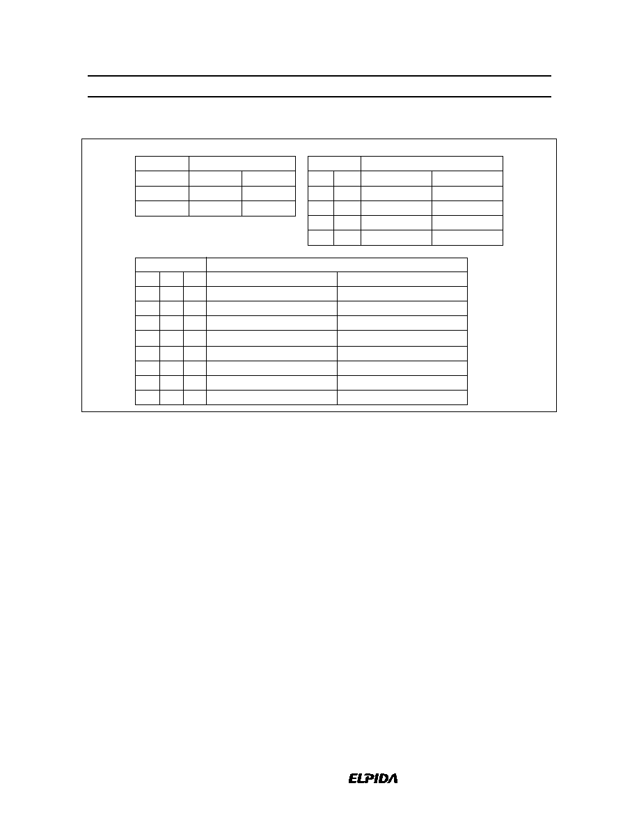
BA1, BA0, A11, A10, A12, A9, A8: (OPCODE): The SDRAM has two types of write modes. One is the
burst write mode, and the other is the single write mode. These bits specify write mode.
Burst read and burst write: Burst write is performed for the specified burst length starting from the column
address specified in the write cycle.
Burst read and single write: Data is only written to the column address specified during the write cycle,
regardless of the burst length.
A7: Keep this bit Low at the mode register set cycle. If this pin is high, the vender test mode is set.
A6, A5, A4: (LMODE): These pins specify the
CAS latency.
A3: (BT): A burst type is specified.
A2, A1, A0: (BL): These pins specify the burst length.
A2 A1
A0
Burst length
0
0
0
1
0
0
1
2
0
1
0
4
0
1
1
8
1
1
1
BT=0
BT=1
1
0
0
R
1
1
0
R
R
1
2
4
8
R
R
R
A3
0 Sequential
1
Interleave
Burst type
A6
A5
A4 CAS latency
0
0
0
R
0
0
1
R
0
1
0
2
0
1
1
3
1
X
X
R
A9
A8
A7
A6
A5
A4
A3
A2
A1
A0
OPCODE
0
LMODE
BT
BL
A9
0
0
R
Write mode
A8
0
1
Burst read and burst write
1
Burst read and single write
0
1
R
1
1
0
1
R
R
R is Reserved (inhibit)
X: 0 or 1
A11
A10
A10
X
X
X
A11
X
X
X
0
0
A12
BA0
BA1
BA1 BA0
X
X
X
0
X
X
X
0
A12
X
X
X
0
HM5259165B/HM5259805B/HM5259405B-75/A6
Data Sheet E0118H10
21
Burst Sequence
A2
A1
A0
Addressing(decimal)
0
0
0
0
0
1
0
1
0
0
1
1
1
1
1
Interleave
Sequential
1
0
0
1
1
0
1
0
1
Starting Ad.
0, 1, 2, 3, 4, 5, 6, 7,
1, 2, 3, 4, 5, 6, 7,
2, 3, 4, 5, 6, 7,
3, 4, 5, 6, 7,
4, 5, 6, 7,
5, 6, 7,
6, 7,
7,
0,
0, 1,
0, 1, 2,
0, 1, 2, 3,
0, 1, 2, 3, 4,
0, 1, 2, 3, 4, 5,
0, 1, 2, 3, 4, 5, 6,
0, 1, 2, 3, 4, 5, 6, 7,
1, 0, 3, 2, 5, 4, 7,
2, 3, 0, 1, 6, 7,
3, 2, 1, 0, 7,
4, 5, 6, 7,
5, 4, 7,
6, 7,
7,
6,
4, 5,
6, 5, 4,
0, 1, 2, 3,
6, 1, 0, 3, 2,
4, 5, 2, 3, 0, 1,
6, 5, 4, 3, 2, 1, 0,
Burst length = 8
A1
A0
Addressing(decimal)
0
0
0
1
1
0
1
1
Interleave
Sequential
Starting Ad.
0, 1, 2, 3,
1, 2, 3, 0,
2, 3, 0, 1,
3, 0, 1, 2,
0, 1, 2, 3,
1, 0, 3, 2,
2, 3, 0, 1,
3, 2, 1, 0,
Burst length = 4
A0
Addressing(decimal)
0
1
Interleave
Sequential
Starting Ad.
0, 1,
1, 0,
0, 1,
1, 0,
Burst length = 2
HM5259165B/HM5259805B/HM5259405B-75/A6
Data Sheet E0118H10
22
Operation of the SDRAM
The following chapter shows operation example of the products below.
Organization
Input/output mask
CAS latency
8-Mword
◊ 16-bit ◊ 4 bank
DQMU/DQML
2/3
16-Mword
◊ 8-bit ◊ 4 bank
DQM
32-Mword
◊ 4-bit ◊ 4 bank
DQM
Note:
The SDRAM should be used according to the product capability (See "Features", "Pin Description"
and "AC Characteristics").
Read/Write Operations
Bank active: Before executing a read or write operation, the corresponding bank and the row address must be
activated by the bank active (ACTV) command. An interval of t
RCD
is required between the bank active
command input and the following read/write command input.
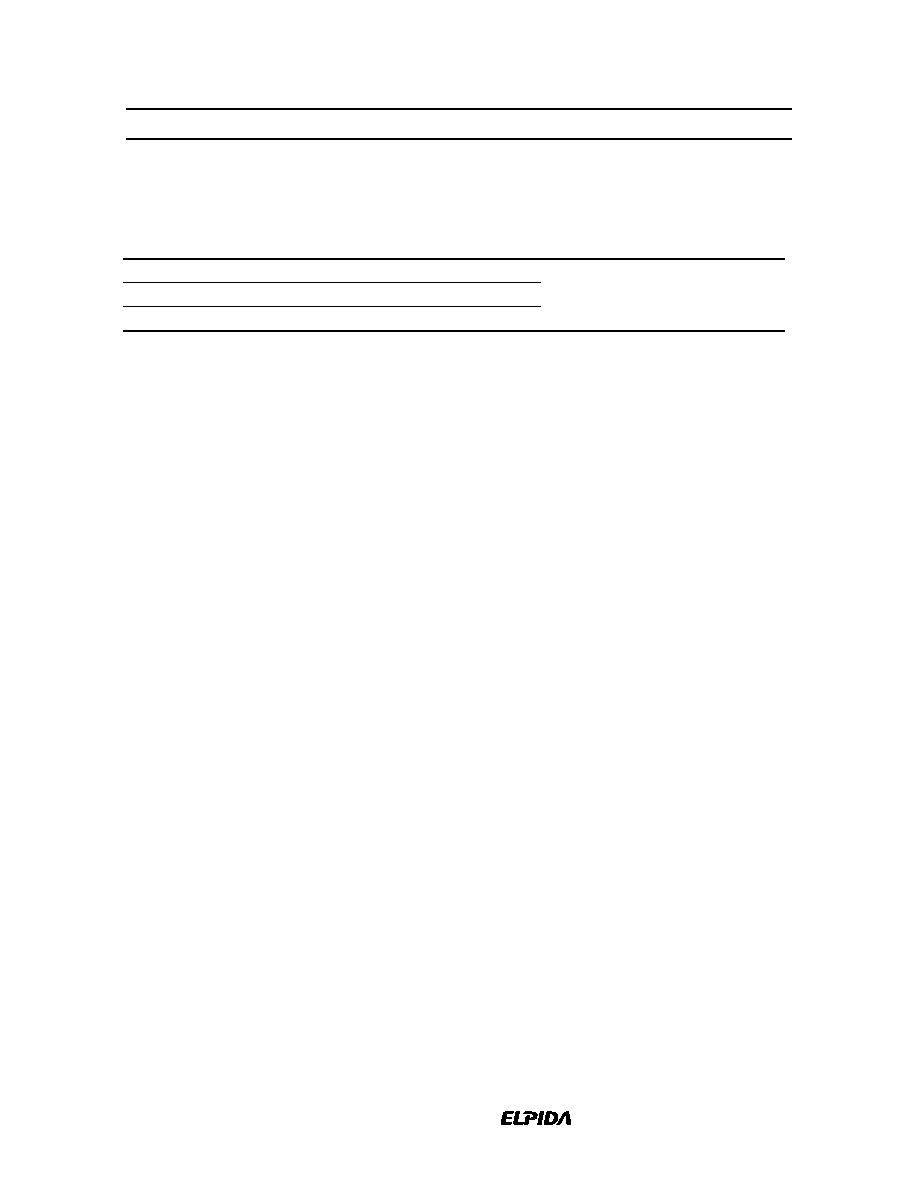
Read operation: A read operation starts when a read command is input. Output buffer becomes Low-Z in
the (
CAS Latency - 1) cycle after read command set. The SDRAM can perform a burst read operation.
The burst length can be set to 1, 2, 4, 8. The start address for a burst read is specified by the column address
and the bank select address (BA0/BA1) at the read command set cycle. In a read operation, data output starts
after the number of clocks specified by the
CAS Latency. The CAS Latency can be set to 2 or 3.
When the burst length is 1, 2, 4, 8, the Dout buffer automatically becomes High-Z at the next clock after the
successive burst-length data has been output.
The
CAS latency and burst length must be specified at the mode register.
HM5259165B/HM5259805B/HM5259405B-75/A6
Data Sheet E0118H10
23
CAS Latency
READ
CLK
Command
Dout
ACTV
Row
Column
Address
CL = 2
CL = 3
out 0
out 1
out 2
out 3
out 0
out 1
out 2
out 3
t
RCD
CL =
CAS latency
Burst Length = 4
Burst Length
READ
CLK
Command
Dout
ACTV
Row
Column
out 0
out 6
out 7
Address
out 0 out 1
out 4
out 5
out 0 out 1 out 2 out 3
BL = 1
out 0 out 1 out 2
out 3
BL = 2
BL = 4
BL = 8
t
RCD
BL : Burst Length
CAS Latency = 2
HM5259165B/HM5259805B/HM5259405B-75/A6
Data Sheet E0118H10
24
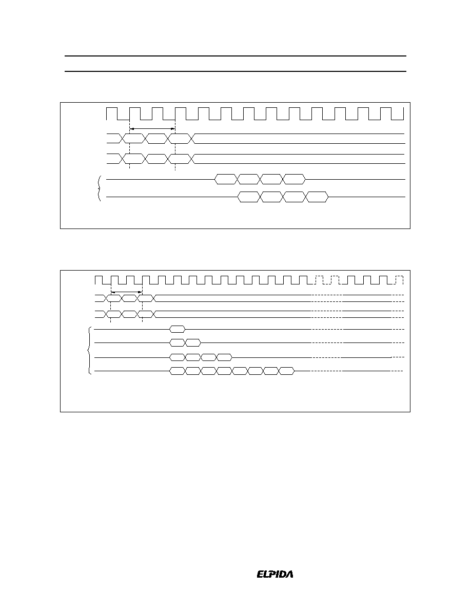
Write operation: Burst write or single write mode is selected by the OPCODE (BA1, BA0, A12, A11, A10,
A9, A8) of the mode register.
1. Burst write: A burst write operation is enabled by setting OPCODE (A9, A8) to (0, 0). A burst write
starts in the same clock as a write command set. (The latency of data input is 0 clock.) The burst length can
be set to 1, 2, 4 and 8, like burst read operations. The write start address is specified by the column address
and the bank select address (BA0/BA1) at the write command set cycle.
WRIT
CLK
Command
Din
ACTV
Row
Column
in 0
in 6
in 7
Address
in 1
in 4
in 5
in 3
BL = 1
BL = 2
BL = 4
BL = 8
t
RCD
in 0
in 0
in 0
in 1
in 1
in 2
in 2
in 3
CAS Latency = 2, 3
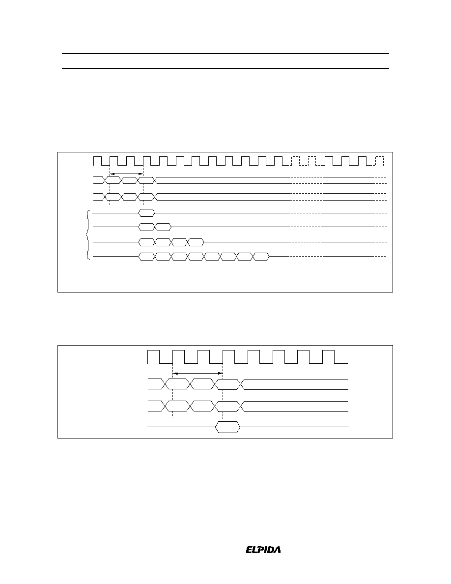
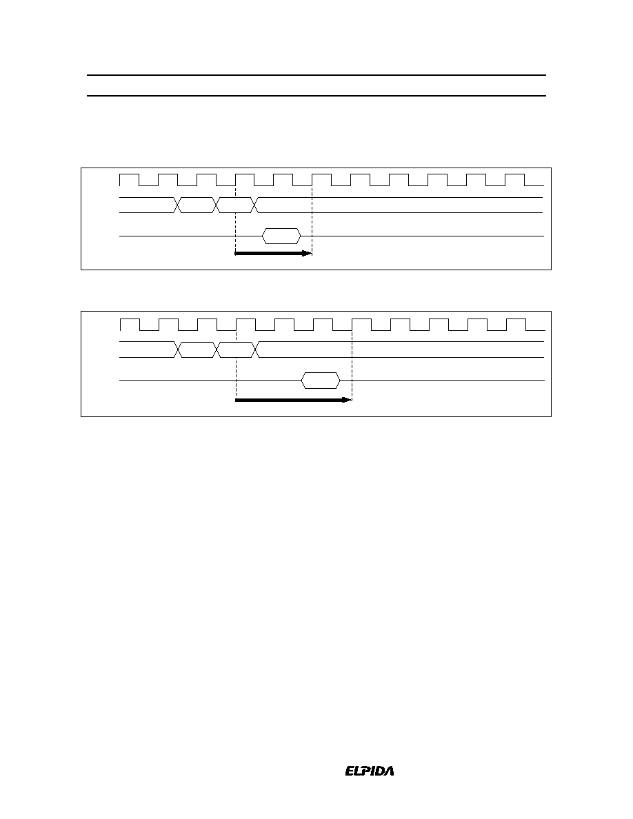
2. Single write: A single write operation is enabled by setting OPCODE (A9, A8) to (1, 0). In a single write
operation, data is only written to the column address and the bank select address (BA0/BA1) specified by the
write command set cycle without regard to the burst length setting. (The latency of data input is 0 clock).
WRIT
CLK
Command
Din
ACTV
Row
Column
in 0
Address
t
RCD
HM5259165B/HM5259805B/HM5259405B-75/A6
Data Sheet E0118H10
25
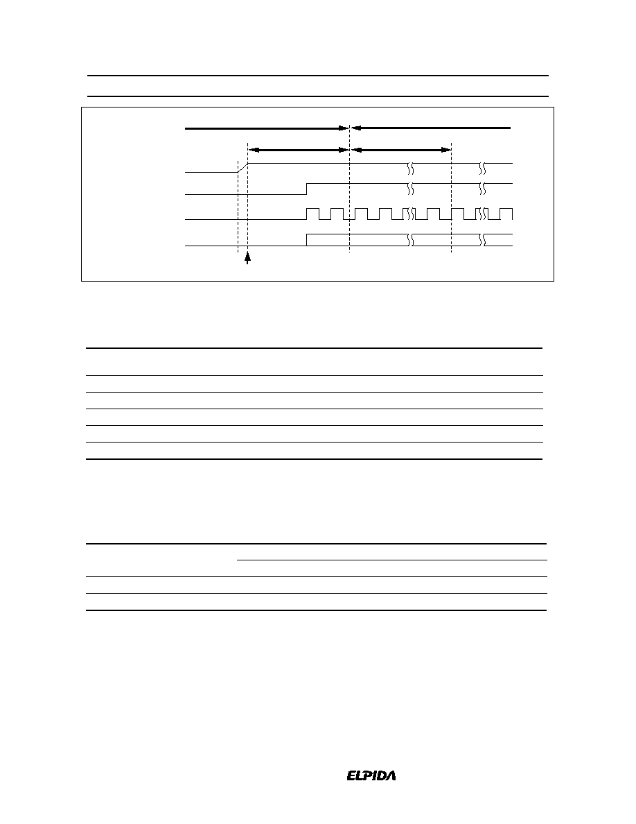
Auto Precharge
Read with auto-precharge: In this operation, since precharge is automatically performed after completing a
read operation, a precharge command need not be executed after each read operation. The command executed
for the same bank after the execution of this command must be the bank active (ACTV) command. In
addition, an interval defined by l
APR
is required before execution of the next command.
CAS latency
Precharge start cycle
3
2 cycle before the final data is output
2
1 cycle before the final data is output
Burst Read (Burst Length = 4)
CLK
lAPR
lRAS
lAPR
CL=2 Command
CL=3 Command
DQ (input)
DQ (input)
Note: Internal auto-precharge starts at the timing indicated by " ".
And an interval of t
RAS
(l
RAS
) is required between previous active (ACTV) command and internal precharge " ".
ACTV
READ A
ACTV
out3
out2
out1
out0
lRAS
ACTV
READ A
ACTV
out3
out2
out1
out0
HM5259165B/HM5259805B/HM5259405B-75/A6
Data Sheet E0118H10
26
Write with auto-precharge: In this operation, since precharge is automatically performed after completing
a burst write or single write operation, a precharge command need not be executed after each write operation.
The command executed for the same bank after the execution of this command must be the bank active
(ACTV) command. In addition, an interval of l
APW
is required between the final valid data input and input of
next command.
Burst Write (Burst Length = 4)
CLK
Command
DQ (input)
l
APW
I
RAS
ACTV
WRIT A
in0
in1
in2
in3
ACTV
Note: Internal auto-precharge starts at the timing indicated by " ".
and an interval of t
RAS
(l
RAS
) is required between previous active (ACTV) command
and internal precharge " ".
Single Write
CLK
Command
DQ (input)
l
APW
I
RAS
ACTV
WRIT A
in
ACTV
Note: Internal auto-precharge starts at the timing indicated by " ".
and an interval of t
RAS
(l
RAS
) is required between previous active (ACTV) command
and internal precharge " ".

HM5259165B/HM5259805B/HM5259405B-75/A6
Data Sheet E0118H10
27
Command Intervals
Read command to Read command interval:
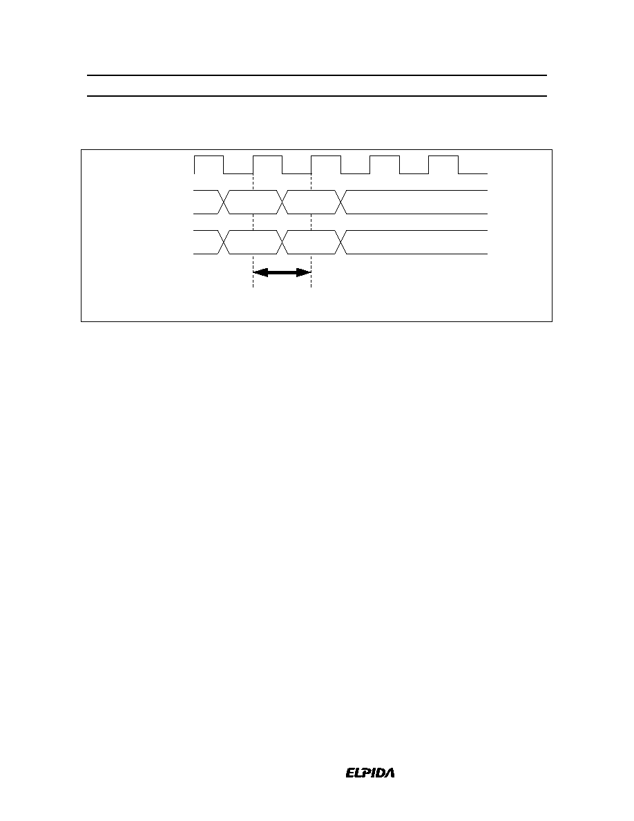
1. Same bank, same ROW address: When another read command is executed at the same ROW address
of the same bank as the preceding read command execution, the second read can be performed after an
interval of no less than 1 clock. Even when the first command is a burst read that is not yet finished, the data
read by the second command will be valid.
READ to READ Command Interval (same ROW address in same bank)
CLK
Command
Dout
out B3
Address
out B1 out B2
BS
ACTV
Row
Column A
READ
READ
Column B
out A0 out B0
Bank0
Active
Column =A
Read
Column =B
Read
Column =A
Dout
Column =B
Dout
CAS Latency = 3
Burst Length = 4
Bank 0
2. Same bank, different ROW address: When the ROW address changes on same bank, consecutive read
commands cannot be executed; it is necessary to separate the two read commands with a precharge command
and a bank-active command.
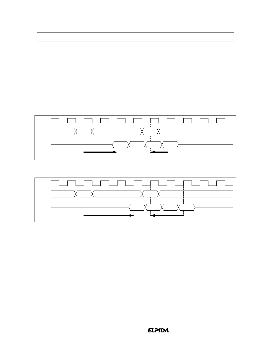
3. Different bank: When the bank changes, the second read can be performed after an interval of no less
than 1 clock, provided that the other bank is in the bank-active state. Even when the first command is a burst
read that is not yet finished, the data read by the second command will be valid.
READ to READ Command Interval (different bank)
CLK
Command
Dout
out B3
Address
out B1 out B2
BS
ACTV
Row 0
Row 1
ACTV
READ
Column A
out A0 out B0
Bank0
Active
Bank3
Active
Bank0
Read
Bank3
Read
READ
Column B
Bank0
Dout
Bank3
Dout
CAS Latency = 3
Burst Length = 4
HM5259165B/HM5259805B/HM5259405B-75/A6
Data Sheet E0118H10
28
Write command to Write command interval:
1. Same bank, same ROW address: When another write command is executed at the same ROW address
of the same bank as the preceding write command, the second write can be performed after an interval of no
less than 1 clock. In the case of burst writes, the second write command has priority.
WRITE to WRITE Command Interval (same ROW address in same bank)
CLK
Command
Din
in B3
Address
in B1
in B2
BS
ACTV
Row
Column A
WRIT
WRIT
Column B
in A0
in B0
Bank0
Active
Column =A
Write
Column =B
Write
Burst Write Mode
Burst Length = 4
Bank 0
2. Same bank, different ROW address: When the ROW address changes, consecutive write commands
cannot be executed; it is necessary to separate the two write commands with a precharge command and a
bank-active command.
3. Different bank: When the bank changes, the second write can be performed after an interval of no less
than 1 clock, provided that the other bank is in the bank-active state. In the case of burst write, the second
write command has priority.
WRITE to WRITE Command Interval (different bank)
CLK
Command
Din
in B3
Address
in B1
in B2
BS
ACTV
Row 0
Row 1
ACTV
WRIT
Column A
in A0
in B0
Bank0
Active
Bank3
Active
Bank0
Write
Bank3
Write
WRIT
Column B
Burst Write Mode
Burst Length = 4
HM5259165B/HM5259805B/HM5259405B-75/A6
Data Sheet E0118H10
29
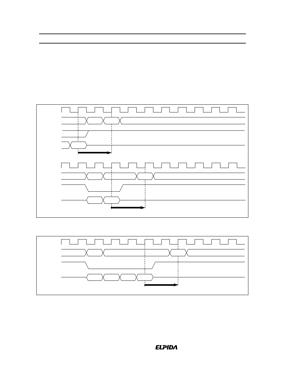
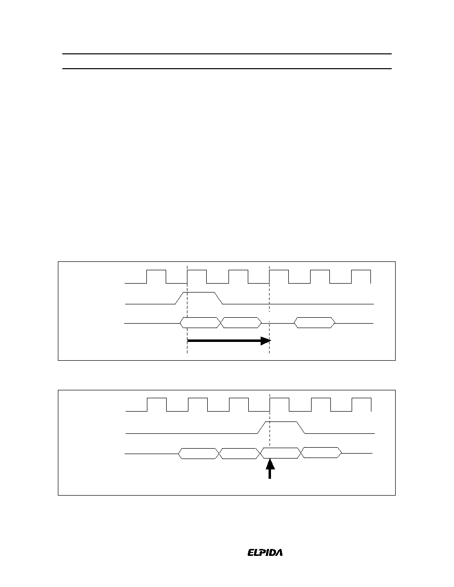
Read command to Write command interval:
1. Same bank, same ROW address: When the write command is executed at the same ROW address of the
same bank as the preceding read command, the write command can be performed after an interval of no less
than 1 clock. However, DQM, DQMU/DQML must be set High so that the output buffer becomes High-Z
before data input.
READ to WRITE Command Interval (1)
CLK
Command
Dout
in B2
in B3
READ WRIT
in B0
in B1
High-Z
Din
CL=2
CL=3
DQM,
DQMU
/DQML
Burst Length = 4
Burst write
READ to WRITE Command Interval (2)
CLK
Command
Dout
READ
WRIT
Din
CL=2
CL=3
DQM,
DQMU/DQML
High-Z
2 clock
High-Z
2. Same bank, different ROW address: When the ROW address changes, consecutive write commands
cannot be executed; it is necessary to separate the two commands with a precharge command and a bank-
active command.
3. Different bank: When the bank changes, the write command can be performed after an interval of no less
than 1 cycle, provided that the other bank is in the bank-active state. However, DQM, DQMU/DQML must
be set High so that the output buffer becomes High-Z before data input.
HM5259165B/HM5259805B/HM5259405B-75/A6
Data Sheet E0118H10
30
Write command to Read command interval:
1. Same bank, same ROW address: When the read command is executed at the same ROW address of the
same bank as the preceding write command, the read command can be performed after an interval of no less
than 1 clock. However, in the case of a burst write, data will continue to be written until one clock before the
read command is executed.
WRITE to READ Command Interval (1)
CLK
Command
Din
WRIT
READ
in A0
out B1
out B2
out B3
out B0
Dout
Column = A
Write
Column = B
Read
Column = B
Dout
CAS Latency
DQM,
DQMU/DQML
Burst Write Mode
CAS Latency = 2
Burst Length = 4
Bank 0
WRITE to READ Command Interval (2)
CLK
Command
Din
WRIT
READ
in A0
out B1
out B2
out B3
out B0
Dout
Column = A
Write
Column = B
Read
Column = B
Dout
CAS Latency
in A1
DQM,
DQMU/DQML
Burst Write Mode
CAS Latency = 2
Burst Length = 4
Bank 0
2. Same bank, different ROW address: When the ROW address changes, consecutive read commands
cannot be executed; it is necessary to separate the two commands with a precharge command and a bank-
active command.
3. Different bank: When the bank changes, the read command can be performed after an interval of no less
than 1 clock, provided that the other bank is in the bank-active state. However, in the case of a burst write,
data will continue to be written until one clock before the read command is executed (as in the case of the
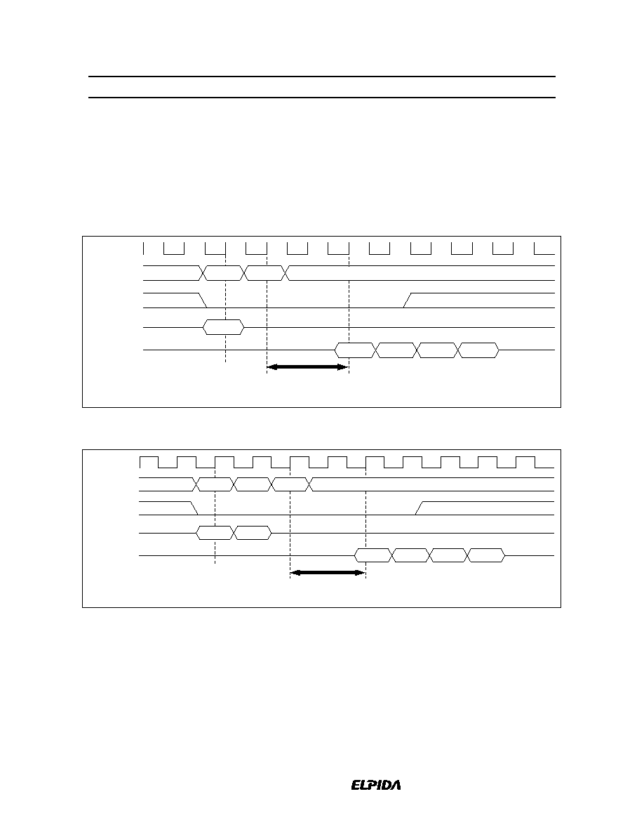
same bank and the same address).
HM5259165B/HM5259805B/HM5259405B-75/A6
Data Sheet E0118H10
31
Read with auto precharge to Read command interval
1. Different bank: When some banks are in the active state, the second read command (another bank) is
executed. Even when the first read with auto-precharge is a burst read that is not yet finished, the data read by
the second command is valid. The internal auto-precharge of one bank starts at the next clock of the second
command.
Read with Auto Precharge to Read Command Interval (Different bank)
CLK
Command
BS
Dout
READ A
READ
out A0
out A1
out B0
out B1
CAS Latency = 3
Burst Length = 4
bank0
Read A
bank3
Read
Note: Internal auto-precharge starts at the timing indicated by " ".
2. Same bank: The consecutive read command (the same bank) is illegal.
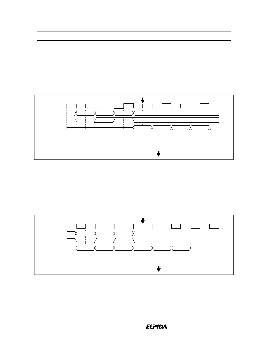
Write with auto precharge to Write command interval
1. Different bank: When some banks are in the active state, the second write command (another bank) is
executed. In the case of burst writes, the second write command has priority. The internal auto-precharge of
one bank starts at the next clock of the second command .
Write with Auto Precharge to Write Command Interval (Different bank)
CLK
Command
BS
Din
WRIT A
WRIT
in B1
in B2
in B3
in A0
in A1
in B0
Burst Length = 4
bank0
Write A
bank3
Write
Note: Internal auto-precharge starts at the timing indicated by " ".
2. Same bank: The consecutive write command (the same bank) is illegal.
HM5259165B/HM5259805B/HM5259405B-75/A6
Data Sheet E0118H10
32
Read with auto precharge to Write command interval
1. Different bank: When some banks are in the active state, the second write command (another bank) is
executed. However, DQM, DQMU/DQML must be set High so that the output buffer becomes High-Z before
data input. The internal auto-precharge of one bank starts at the next clock of the second command.
Read with Auto Precharge to Write Command Interval (Different bank)
CLK
Command
BS
Dout
Din
CL = 2
CL = 3
READ A
WRIT
in B0
in B1
in B2
in B3
Burst Length = 4
bank0
Read A
bank3
Write
Note: Internal auto-precharge starts at the timing indicated by " ".
DQM,
DQMU/DQML
High-Z
2. Same bank: The consecutive write command from read with auto precharge (the same bank) is illegal. It
is necessary to separate the two commands with a bank active command.
HM5259165B/HM5259805B/HM5259405B-75/A6
Data Sheet E0118H10
33
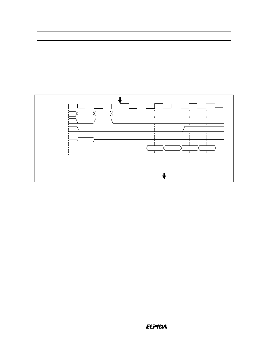
Write with auto precharge to Read command interval
1. Different bank: When some banks are in the active state, the second read command (another bank) is
executed. However,in case of a burst write, data will continue to be written until one clock before the read
command is executed. The internal auto-precharge of one bank starts at the next clock of the second
command.
Write with Auto Precharge to Read Command Interval (Different bank)
CLK
Command
BS
Dout
Din
WRIT A
READ
out B0
out B1
out B2
out B3
CAS Latency = 3
Burst Length = 4
bank0
Write A
bank3
Read
Note: Internal auto-precharge starts at the timing indicated by " ".
DQM,
DQMU/DQML
in A0
2. Same bank: The consecutive read command from write with auto precharge (the same bank) is illegal. It
is necessary to separate the two commands with a bank active command.
HM5259165B/HM5259805B/HM5259405B-75/A6
Data Sheet E0118H10
34
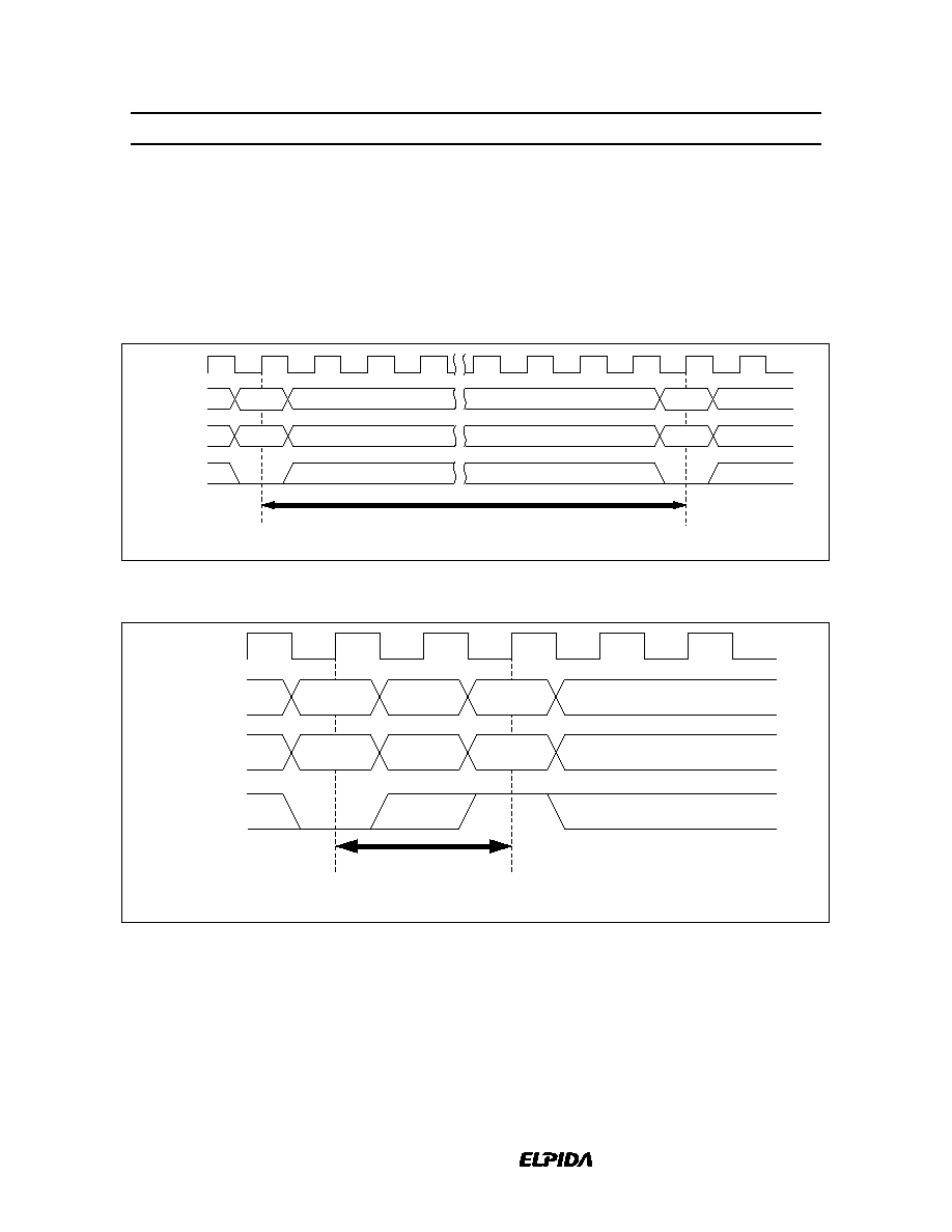
Read command to Precharge command interval (same bank):
When the precharge command is executed for the same bank as the read command that preceded it, the
minimum interval between the two commands is one clock. However, since the output buffer then becomes
High-Z after the clocks defined by l
HZP
, there is a case of interruption to burst read data output will be
interrupted, if the precharge command is input during burst read. To read all data by burst read, the clocks
defined by l
EP
must be assured as an interval from the final data output to precharge command execution.
READ to PRECHARGE Command Interval (same bank): To output all data
CAS Latency = 2, Burst Length = 4
CLK
Command
Dout
READ
PRE/PALL
out A0
out A1
out A2
out A3
CL=2
l = -1 cycle
EP
CAS Latency = 3, Burst Length = 4
CLK
Command
Dout
READ
PRE/PALL
out A0
out A1
out A2
out A3
CL=3
l = -2 cycle
EP
HM5259165B/HM5259805B/HM5259405B-75/A6
Data Sheet E0118H10
35
READ to PRECHARGE Command Interval (same bank): To stop output data
CAS Latency = 2, Burst Length = 1, 2, 4, 8
CLK
Command
Dout
READ
PRE/PALL
out A0
l
HZP
=2
High-Z
CAS Latency = 3, Burst Length = 1, 2, 4, 8
CLK
Command
Dout
READ
PRE/PALL
out A0
l
HZP
=3
High-Z
HM5259165B/HM5259805B/HM5259405B-75/A6
Data Sheet E0118H10
36
Write command to Precharge command interval (same bank): When the precharge command is executed
for the same bank as the write command that preceded it, the minimum interval between the two commands is
1 clock. However, if the burst write operation is unfinished, the input data must be masked by means of
DQM, DQMU/DQML for assurance of the clock defined by t
DPL
.
WRITE to PRECHARGE Command Interval (same bank)
Burst Length = 4 (To stop write operation)
CLK
Command
Din
WRIT
PRE/PALL
t
DPL
DQM,
DQMU/DQML
CLK
in A0
in A1
Command
Din
WRIT
PRE/PALL
DQM,
DQMU/DQML
t
DPL
Burst Length = 4 (To write all data)
CLK
in A0
in A1
in A2
Command
Din
WRIT
PRE/PALL
in A3
DQM,
DQMU/DQML
t
DPL
HM5259165B/HM5259805B/HM5259405B-75/A6
Data Sheet E0118H10
37
Bank active command interval:
1. Same bank: The interval between the two bank-active commands must be no less than t
RC
.
2. In the case of different bank-active commands: The interval between the two bank-active commands
must be no less than t
RRD
.
Bank Active to Bank Active for Same Bank
CLK
Command
Address
BS
Bank 0
Active
ACTV
ROW
ACTV
ROW
Bank 0
Active
t
RC
Bank Active to Bank Active for Different Bank
CLK
Command
Address
BS
Bank 0
Active
Bank 3
Active
ACTV
ROW:0
ACTV
ROW:1
t
RRD
HM5259165B/HM5259805B/HM5259405B-75/A6
Data Sheet E0118H10
38
Mode register set to Bank-active command interval: The interval between setting the mode register and
executing a bank-active command must be no less than l
RSA
.
CLK
Command
Address
Mode
Register Set
Bank
Active
MRS
ACTV
I
RSA
BS & ROW
CODE
HM5259165B/HM5259805B/HM5259405B-75/A6
Data Sheet E0118H10
39
DQM Control
The DQM mask the DQ data. The DQMU and DQML mask the upper and lower bytes of the DQ data,
respectively. The timing of DQMU/DQML is different during reading and writing.
Reading: When data is read, the output buffer can be controlled by DQM, DQMU/DQML. By setting
DQM, DQMU/DQML to Low, the output buffer becomes Low-Z, enabling data output. By setting DQM,
DQMU/DQML to High, the output buffer becomes High-Z, and the corresponding data is not output.
However, internal reading operations continue. The latency of DQM, DQMU/DQML during reading is 2
clocks.
Writing: Input data can be masked by DQM, DQMU/DQML. By setting DQM, DQMU/DQML to Low,
data can be written. In addition, when DQM, DQMU/DQML is set to High, the corresponding data is not
written, and the previous data is held. The latency of DQM, DQMU/DQML during writing is 0 clock.
Reading
CLK
DQ (output)
out 0
out 1
l = 2 Latency
out 3
DOD
DQM,
DQMU/DQML
High-Z
Writing
CLK
DQ (input)
in 0
in 1
l = 0 Latency
in 3
;;
;
DID
DQM,
DQMU/DQML

HM5259165B/HM5259805B/HM5259405B-75/A6
Data Sheet E0118H10
40
Refresh
Auto-refresh: All the banks must be precharged before executing an auto-refresh command. Since the auto-
refresh command updates the internal counter every time it is executed and determines the banks and the
ROW addresses to be refreshed, external address specification is not required. The refresh cycle is 8192
cycles/32 ms. (8192 cycles are required to refresh all the ROW addresses.) The output buffer becomes High-
Z after auto-refresh start. In addition, since a precharge has been completed by an internal operation after the
auto-refresh, an additional precharge operation by the precharge command is not required.
Self-refresh: After executing a self-refresh command, the self-refresh operation continues while CKE is held
Low. During self-refresh operation, all ROW addresses are refreshed by the internal refresh timer. A self-
refresh is terminated by a self-refresh exit command. Before and after self-refresh mode, execute auto-refresh
to all refresh addresses in or within 32 ms period on the condition (1) and (2) below.
(1) Enter self-refresh mode within 3.9 µs after either burst refresh or distributed refresh at equal interval to all
refresh addresses are completed.
(2) Start burst refresh or distributed refresh at equal interval to all refresh addresses within 3.9 µs after exiting
from self-refresh mode.
Others
Power-down mode: The SDRAM enters power-down mode when CKE goes Low in the IDLE state. In
power down mode, power consumption is suppressed by deactivating the input initial circuit. Power down
mode continues while CKE is held Low. In addition, by setting CKE to High, the SDRAM exits from the
power down mode, and command input is enabled from the next clock. In this mode, internal refresh is not
performed.
Clock suspend mode: By driving CKE to Low during a bank-active or read/write operation, the SDRAM
enters clock suspend mode. During clock suspend mode, external input signals are ignored and the internal
state is maintained. When CKE is driven High, the SDRAM terminates clock suspend mode, and command
input is enabled from the next clock. For details, refer to the "CKE Truth Table".
Power-up sequence: The SDRAM should be goes on the following sequence with power up.
The CLK, CKE,
CS, DQM, DQMU/DQML and DQ pins keep low till power stabilizes.
The CLK pin is stabilized within 100 µs after power stabilizes before the following initialization sequence.
The CKE and DQM, DQMU/DQML is driven to high between power stabilizes and the initialization
sequence.
This SDRAM has V
CC
clamp diodes for CLK, CKE,
CS DQM, DQMU/DQML and DQ pins. If these pins go
high before power up, the large current flows from these pins to V
CC
through the diodes.
Initialization sequence: When 200 µs or more has past after the above power-up sequence, all banks must be
precharged using the precharge command (PALL). After t
RP
delay, set 8 or more auto refresh commands
(REF). Set the mode register set command (MRS) to initialize the mode register. We recommend that by
keeping DQM, DQMU/DQML and CKE to High, the output buffer becomes High-Z during Initialization
sequence, to avoid DQ bus contention on memory system formed with a number of device.
HM5259165B/HM5259805B/HM5259405B-75/A6
Data Sheet E0118H10
41
V
CC
, V
CC
Q
Power up sequence
Initialization sequence
100
µs
0 V
Low
Low
Low
CKE, DQM,
DQMU/DQML
CLK
CS, DQ
200
µs
Power stabilize
Absolute Maximum Ratings
Parameter
Symbol
Value
Unit
Note
Voltage on any pin relative to V
SS
V
T
≠0.5 to V
CC
+ 0.5
(
4.6 (max))
V
1
Supply voltage relative to V
SS
V
CC
≠0.5 to +4.6
V
1
Short circuit output current
Iout
50
mA
Power dissipation
P
T
1.2
W
Operating temperature
Topr
0 to +70
∞C
Storage temperature
Tstg
≠55 to +125
∞C
Note:
1. Respect to V
SS
.
DC Operating Conditions (Ta = 0 to +70∞C)
Parameter
Symbol
Min
Max
Unit
Notes
Supply voltage
V
CC
, V
CC
Q
3.0
3.6
V
1, 2
V
SS
, V
SS
Q
0
0
V
3
Input high voltage
V
IH
2.0
V
CC
+ 0.3
V
1, 4
Input low voltage
V
IL
≠0.3
0.8
V
1, 5
Notes: 1. All voltage referred to V
SS
.
2. The supply voltage with all V
CC
and V
CC
Q pins must be on the same level.
3. The supply voltage with all V
SS
and V
SS
Q pins must be on the same level.
4. V
IH
(max) = V
CC
+ 2.0 V for pulse width
3 ns at V
CC
.
5. V
IL
(min) = V
SS
≠ 2.0 V for pulse width
3 ns at V
SS
.
HM5259165B/HM5259805B/HM5259405B-75/A6
Data Sheet E0118H10
42
V
IL
/V
IH
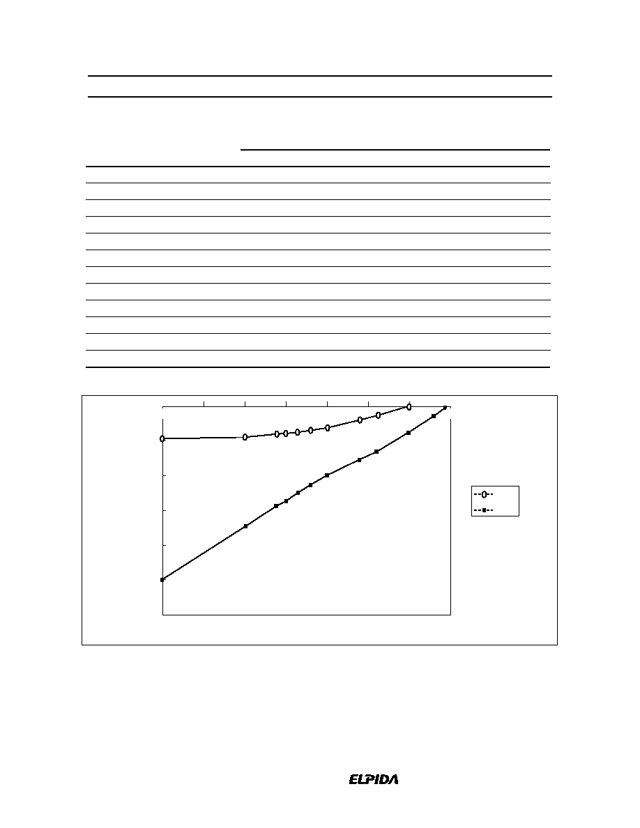
Clamp
This SDRAM has V
IL
and V
IH
clamp for CLK, CKE, CS, DQM and I/O pins.
Minimum V
IL
Clamp Current
V
IL
(V)
I (mA)
≠2
≠32
≠1.8
≠25
≠1.6
≠19
≠1.4
≠13
≠1.2
≠8
≠1
≠4
≠0.9
≠2
≠0.8
≠0.6
≠0.6
0
≠0.4
0
≠0.2
0
0
0
V
IL
(V)
I (mA)
≠1.5
≠1
≠0.5
≠5
≠15
≠10
≠25
≠20
≠30
0
≠35
≠2
0
HM5259165B/HM5259805B/HM5259405B-75/A6
Data Sheet E0118H10
43
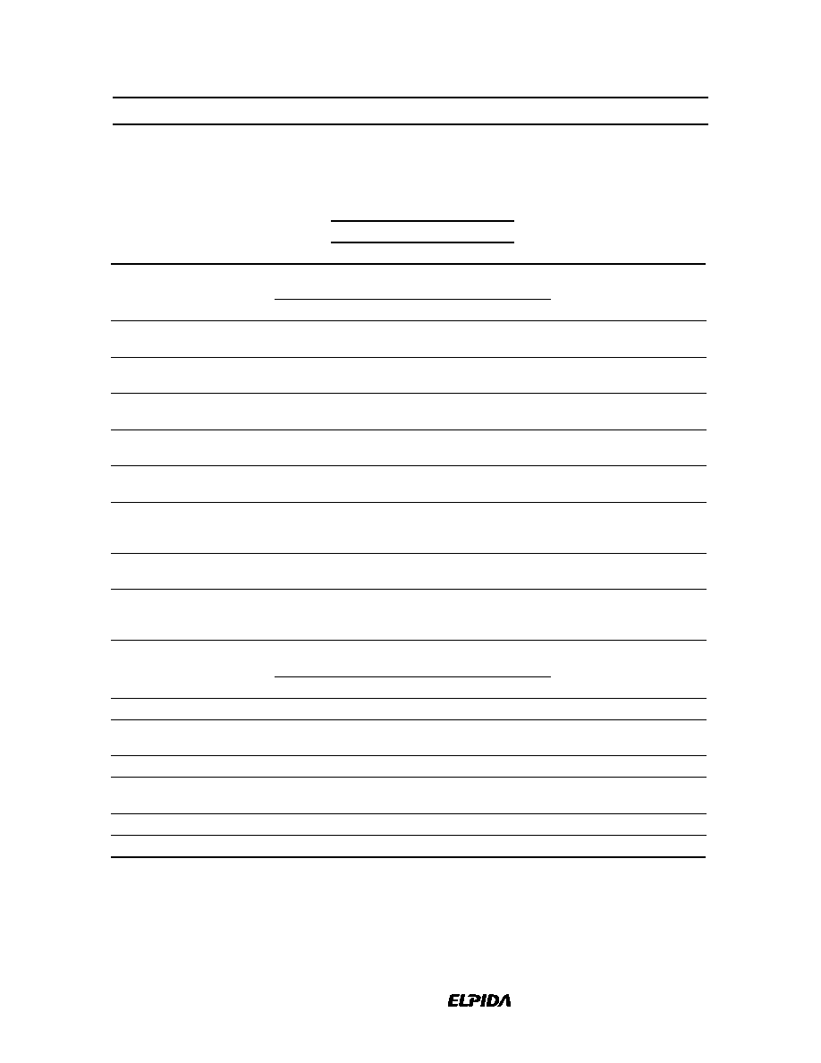
Minimum V
IH
Clamp Current
V
IH
(V)
I (mA)
V
CC
+ 2
10
V
CC
+ 1.8
8
V
CC
+ 1.6
5.5
V
CC
+ 1.4
3.5
V
CC
+ 1.2
1.5
V
CC
+ 1
0.3
V
CC
+ 0.8
0
V
CC
+ 0.6
0
V
CC
+ 0.4
0
V
CC
+ 0.2
0
V
CC
+ 0
0
V
IH
(V)
V
CC
+ 0
V
CC
+ 1
V
CC
+ 2
V
CC
+ 0.5
V
CC
+ 1.5
I (mA)
8
4
6
0
2
10
HM5259165B/HM5259805B/HM5259405B-75/A6
Data Sheet E0118H10
44
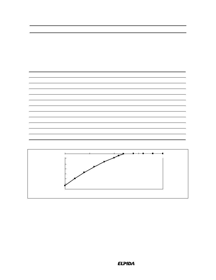
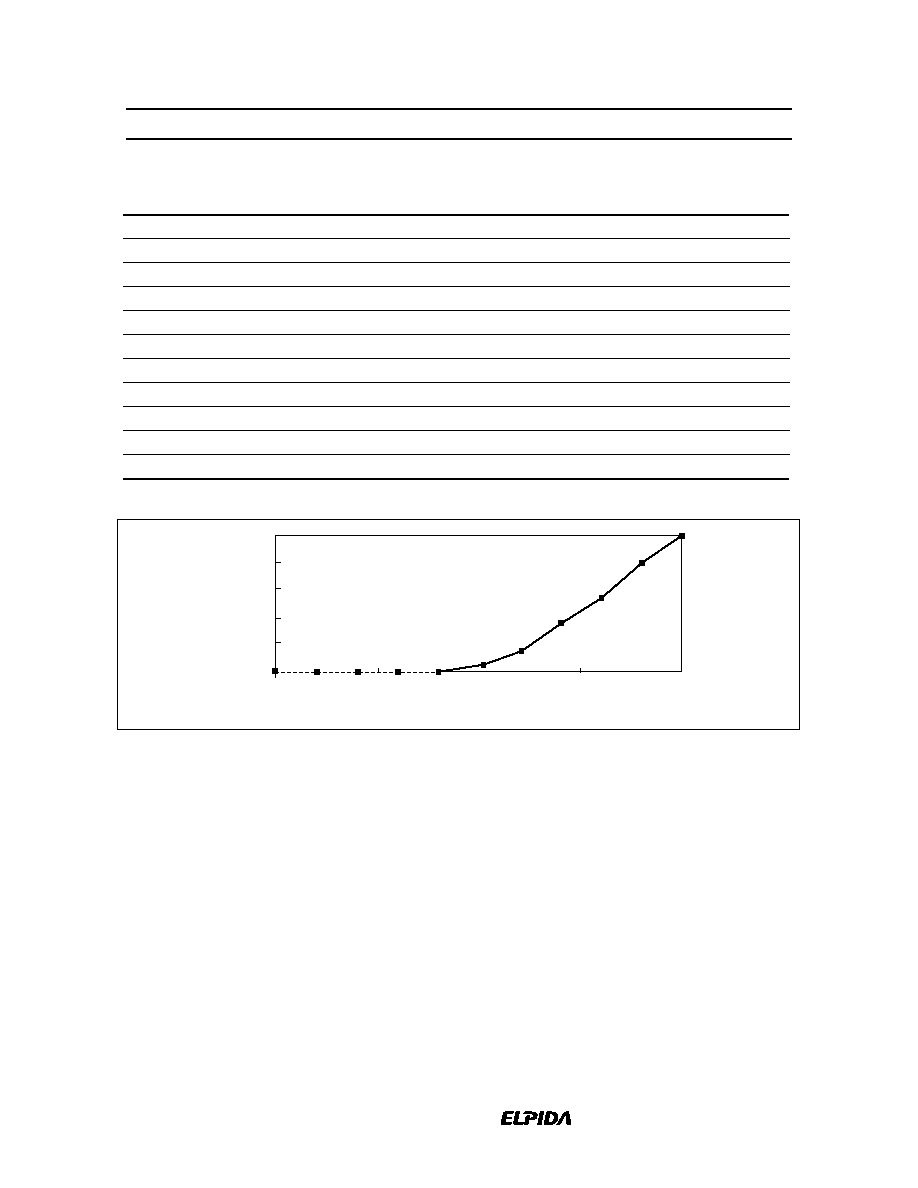
I
OL
/I
OH
Characteristics
Output Low Current (I
OL
)
I
OL
I
OL
Vout (V)
Min (mA)
Max (mA)
0
0
0
0.4
27
71
0.65
41
108
0.85
51
134
1
58
151
1.4
70
188
1.5
72
194
1.65
75
203
1.8
77
209
1.95
77
212
3
80
220
3.45
81
223
I
OL
(mA)
Vout (V)
250
200
150
100
50
0
0
0.5
1
1.5
2
2.5
3
3.5
min
max
HM5259165B/HM5259805B/HM5259405B-75/A6
Data Sheet E0118H10
45
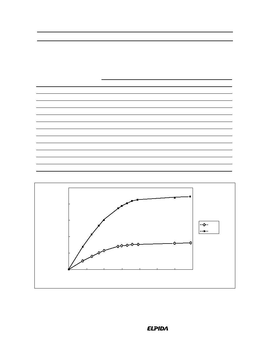
Output High Current (I
OH
) (Ta = 0 to +70∞C, V
CC
, V
CC
Q = 3.0 V to 3.45 V, V
SS
, V
SS
Q = 0 V)
I
OH
I
OH
Vout (V)
Min (mA)
Max (mA)
3.45
--
≠3
3.3
--
≠28
3
0
≠75
2.6
≠21
≠130
2.4
≠34
≠154
2
≠59
≠197
1.8
≠67
≠227
1.65
≠73
≠248
1.5
≠78
≠270
1.4
≠81
≠285
1
≠89
≠345
0
≠93
≠503
I
OH
(mA)
Vout (V)
0
≠100
≠200
≠300
≠500
≠600
≠400
0.5
1
1.5
2
2.5
3
min
max
3.5
0
HM5259165B/HM5259805B/HM5259405B-75/A6
Data Sheet E0118H10
46
DC Characteristics (Ta = 0 to +70∞C, V
CC
, V
CC
Q = 3.3 V ± 0.3 V, V
S S
, V
SS
Q = 0 V)
(HM5259165B)
HM5259165B
-75
-A6
Parameter
Symbol
Min
Max
Min
Max
Unit
Test conditions
Notes
Operating current
(
CAS latency = 2)
I
CC1
--
220
--
190
mA
Burst length = 1
t
RC
= min
1, 2, 3
(
CAS latency = 3)
I
CC1
--
220
--
190
mA
Standby current in power
down
I
CC2P
--
6
--
6
mA
CKE = V
IL
,
t
CK
= 12 ns
6
Standby current in power
down (input signal stable)
I
CC2PS
--
4
--
4
mA
CKE = V
IL
, t
CK
=
7
Standby current in non power
down
I
CC2N
--
40
--
40
mA
CKE,
CS = V
IH
,
t
CK
= 12 ns
4
Standby current in non power
down (input signal stable)
I
CC2NS
--
18
--
18
mA
CKE = V
IH
, t
CK
=
9
Active standby current in
power down
I
CC3P
--
8
--
8
mA
CKE = V
IL
,
t
CK
= 12 ns
1, 2, 6
Active standby current in
power down (input signal
stable)
I
CC3PS
--
6
--
6
mA
CKE = V
IL
, t
CK
=
2, 7
Active standby current in non
power down
I
CC3N
--
60
--
60
mA
CKE,
CS = V
IH
,
t
CK
= 12 ns
1, 2, 4
Active standby current in non
power down (input signal
stable)
I
CC3NS
--
30
--
30
mA
CKE = V
IH
, t
CK
=
2, 9
Burst operating current
(
CAS latency = 2)
I
CC4
--
200
--
200
mA
t
CK
= min, BL = 4
1, 2, 5
(
CAS latency = 3)
I
CC4
--
270
--
200
mA
Refresh current
I
CC5
--
330
--
330
mA
t
RC
= min
3
Self refresh current
I
CC6
--
6
--
6
mA
V
IH
V
CC
≠ 0.2 V
V
IL
0.2 V
8
Input leakage current
I
LI
≠1
1
≠1
1
µA
0
Vin V
CC
Output leakage current
I
LO
≠1.5
1.5
≠1.5
1.5
µA
0
Vout V
CC
DQ = disable
Output high voltage
V
OH
2.4
--
2.4
--
V
I
OH
= ≠4 mA
Output low voltage
V
OL
--
0.4
--
0.4
V
I
OL
= 4 mA
HM5259165B/HM5259805B/HM5259405B-75/A6
Data Sheet E0118H10
47
DC Characteristics (Ta = 0 to +70∞C, V
CC
, V
CC
Q = 3.3 V ± 0.3 V, V
S S
, V
SS
Q = 0 V)
(HM5259805B)
HM5259805B
-75
-A6
Parameter
Symbol
Min
Max
Min
Max
Unit
Test conditions
Notes
Operating current
(
CAS latency = 2)
I
CC1
--
220
--
190
mA
Burst length = 1
t
RC
= min
1, 2, 3
(
CAS latency = 3)
I
CC1
--
220
--
190
mA
Standby current in power
down
I
CC2P
--
6
--
6
mA
CKE = V
IL
,
t
CK
= 12 ns
6
Standby current in power
down (input signal stable)
I
CC2PS
--
4
--
4
mA
CKE = V
IL
, t
CK
=
7
Standby current in non
power down
I
CC2N
--
40
--
40
mA
CKE,
CS = V
IH
,
t
CK
= 12 ns
4
Standby current in non
power down (input signal
stable)
I
CC2NS
--
18
--
18
mA
CKE = V
IH
, t
CK
=
9
Active standby current in
power down
I
CC3P
--
8
--
8
mA
CKE = V
IL
,
t
CK
= 12 ns
1, 2, 6
Active standby current in
power down (input signal
stable)
I
CC3PS
--
6
--
6
mA
CKE = V
IL
, t
CK
=
2, 7
Active standby current in
non power down
I
CC3N
--
60
--
60
mA
CKE,
CS = V
IH
,
t
CK
= 12 ns
1, 2, 4
Active standby current in
non power down (input
signal stable)
I
CC3NS
--
30
--
30
mA
CKE = V
IH
, t
CK
=
2, 9
Burst operating current
(
CAS latency = 2)
I
CC4
--
190
--
190
mA
t
CK
= min, BL = 4
1, 2, 5
(
CAS latency = 3)
I
CC4
--
260
--
190
mA
Refresh current
I
CC5
--
330
--
330
mA
t
RC
= min
3
Self refresh current
I
CC6
--
6
--
6
mA
V
IH
V
CC
≠ 0.2 V
V
IL
0.2 V
8
Input leakage current
I
LI
≠1
1
≠1
1
µA
0
Vin V
CC
Output leakage current
I
LO
≠1.5
1.5
≠1.5
1.5
µA
0
Vout V
CC
DQ = disable
Output high voltage
V
OH
2.4
--
2.4
--
V
I
OH
= ≠4 mA
Output low voltage
V
OL
--
0.4
--
0.4
V
I
OL
= 4 mA

HM5259165B/HM5259805B/HM5259405B-75/A6
Data Sheet E0118H10
48
DC Characteristics (Ta = 0 to +70∞C, V
CC
, V
CC
Q = 3.3 V ± 0.3 V, V
S S
, V
SS
Q = 0 V)
(HM5259405B)
HM5259405B
-75
-A6
Parameter
Symbol
Min
Max
Min
Max
Unit
Test conditions
Notes
Operating current
(
CAS latency = 2)
I
CC1
--
220
--
190
mA
Burst length = 1
t
RC
= min
1, 2, 3
(
CAS latency = 3)
I
CC1
--
220
--
190
mA
Standby current in power
down
I
CC2P
--
6
--
6
mA
CKE = V
IL
,
t
CK
= 12 ns
6
Standby current in power
down (input signal stable)
I
CC2PS
--
4
--
4
mA
CKE = V
IL
, t
CK
=
7
Standby current in non power
down
I
CC2N
--
40
--
40
mA
CKE,
CS = V
IH
,
t
CK
= 12 ns
4
Standby current in non power
down (input signal stable)
I
CC2NS
--
18
--
18
mA
CKE = V
IH
, t
CK
=
9
Active standby current in
power down
I
CC3P
--
8
--
8
mA
CKE = V
IL
,
t
CK
= 12 ns
1, 2, 6
Active standby current in
power down (input signal
stable)
I
CC3PS
--
6
--
6
mA
CKE = V
IL
, t
CK
=
2, 7
Active standby current in non
power down
I
CC3N
--
60
--
60
mA
CKE,
CS = V
IH
,
t
CK
= 12 ns
1, 2, 4
Active standby current in non
power down (input signal
stable)
I
CC3NS
--
30
--
30
mA
CKE = V
IH
, t
CK
=
2, 9
Burst operating current
(
CAS latency = 2)
I
CC4
--
190
--
190
mA
t
CK
= min, BL = 4
1, 2, 5
(
CAS latency = 3)
I
CC4
--
260
--
190
mA
Refresh current
I
CC5
--
330
--
330
mA
t
RC
= min
3
Self refresh current
I
CC6
--
6
--
6
mA
V
IH
V
CC
≠ 0.2 V
V
IL
0.2 V
8
Input leakage current
I
LI
≠1
1
≠1
1
µA
0
Vin V
CC
Output leakage current
I
LO
≠1.5
1.5
≠1.5
1.5
µA
0
Vout V
CC
DQ = disable
Output high voltage
V
OH
2.4
--
2.4
--
V
I
OH
= ≠4 mA
Output low voltage
V
OL
--
0.4
--
0.4
V
I
OL
= 4 mA

HM5259165B/HM5259805B/HM5259405B-75/A6
Data Sheet E0118H10
49
Notes: 1. I
CC
depends on output load condition when the device is selected. I
CC
(max) is specified at the
output open condition.
2. One bank operation.
3. Input signals are changed once per one clock.
4. Input signals are changed once per two clocks.
5. Input signals are changed once per four clocks.
6. After power down mode, CLK operating current.
7. After power down mode, no CLK operating current.
8. After self refresh mode set, self refresh current.
9. Input signals are V
IH
or V
IL
fixed.
Capacitance (Ta = 25∞C, V
CC
, V
CC
Q = 3.3 V ± 0.3 V)
Parameter
Symbol
Min
Max
Unit
Notes
Input capacitance (CLK)
C
I1
2.5
7
pF
1, 2, 4
Input capacitance (Input)
C
I2
2.5
7
pF
1, 2, 4
Output capacitance (DQ)
C
O
4
8
pF
1, 2, 3, 4
Notes: 1. Capacitance measured with Boonton Meter or effective capacitance measuring method.
2. Measurement condition: f = 1 MHz, 1.4 V bias, 200 mV swing.
3. DQM, DQMU/DQML = V
IH
to disable Dout.
4. This parameter is sampled and not 100% tested.
HM5259165B/HM5259805B/HM5259405B-75/A6
Data Sheet E0118H10
50
AC Characteristics (Ta = 0 to +70∞C, V
CC
, V
CC
Q = 3.3 V ± 0.3 V, V
SS
, V
SS
Q = 0 V)
HM5259165B/
HM5259805B/
HM5259405B
-75
-A6
Parameter
Symbol
PC/100
Symbol
Min
Max
Min
Max
Unit
Notes
System clock cycle time
(
CAS latency = 2)
t
CK
Tclk
10
--
10
--
ns
1
(
CAS latency = 3)
t
CK
Tclk
7.5
--
10
--
ns
CLK high pulse width
t
CKH
Tch
2.5
--
3
--
ns
1
CLK low pulse width
t
CKL
Tcl
2.5
--
3
--
ns
1
Access time from CLK
(
CAS latency = 2)
t
AC
Tac
--
6
--
6
ns
1, 2
(
CAS latency = 3)
t
AC
Tac
--
5.4
--
6
ns
Data-out hold time
t
OH
Toh
2.7
--
3
--
ns
1, 2
CLK to Data-out low impedance
t
LZ
2
--
2
--
ns
1, 2, 3
CLK to Data-out high impedance
(
CAS latency = 2, 3)
t
HZ
--
5.4
--
6
ns
1, 4
Input setup time
t
AS
, t
CS
, t
DS
,
t
CES
Tsi
1.5
--
2
--
ns
1, 5, 6
CKE setup time for power down
exit
t
CESP
Tpde
1.5
--
2
--
ns
1
Input hold time
t
AH
, t
CH
, t
DH
,
t
CEH
Thi
0.8
--
1
--
ns
1, 5
Ref/Active to Ref/Active
command period
t
RC
Trc
67.5
--
70
--
ns
1
Active to Precharge command
period
t
RAS
Tras
45
120000 50
120000 ns
1
Active command to column
command (same bank)
t
RCD
Trcd
20
--
20
--
ns
1
Precharge to active command
period
t
RP
Trp
20
--
20
--
ns
1
Write recovery or data-in to
precharge lead time
t
DPL
Tdpl
15
--
20
--
ns
1
Active (a) to Active (b) command
period
t
RRD
Trrd
15
--
20
--
ns
1
Transition time (rise and fall)
t
T
1
5
1
5
ns
Refresh period
t
REF
--
32
--
32
ms
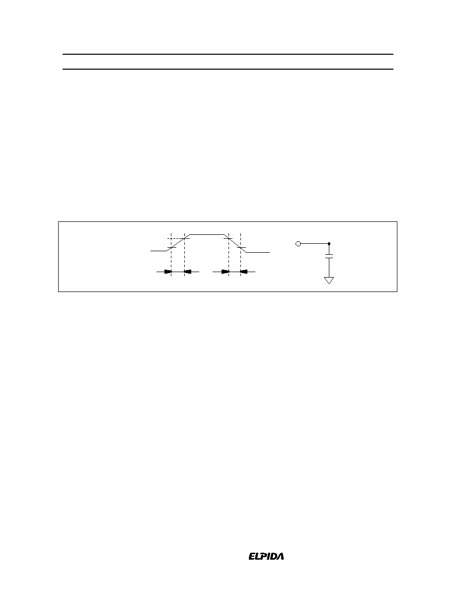
HM5259165B/HM5259805B/HM5259405B-75/A6
Data Sheet E0118H10
51
Notes: 1. AC measurement assumes t
T
= 1 ns. Reference level for timing of input signals is 1.5 V.
2. Access time is measured at 1.5 V. Load condition is CL = 50 pF.
3. t
LZ
(min) defines the time at which the outputs achieves the low impedance state.
4. t
HZ
(max) defines the time at which the outputs achieves the high impedance state.
5. t
CES
define CKE setup time to CLK rising edge except power down exit command.
6. t
AS
/t
AH
: Address, t
CS
/t
CH
:
CS, RAS, CAS, WE, DQM, DQMU/DQML.
t
DS
/t
DH
: Data-in, t
CES
/t
CEH
: CKE.
Test Conditions
∑ Input and output timing reference levels: 1.5 V
∑ Input waveform and output load: See following figures
t
T
2.4 V
0.4 V
0.8 V
2.0 V
input
t
T
I/O
CL

HM5259165B/HM5259805B/HM5259405B-75/A6
Data Sheet E0118H10
52
Relationship Between Frequency and Minimum Latency
HM5259165B/
HM5259805B/
HM5259405B
Parameter
-75
-A6
Frequency (MHz)
133
100
t
CK
(ns)
Symbol
PC/100
Symbol
7.5
10
Notes
Active command to column command
(same bank)
l
RCD
3
2
1
Active command to active command
(same bank)
l
RC
9
7
= [l
RAS
+ l
RP
]
1
Active command to precharge command
(same bank)
l
RAS
6
5
1
Precharge command to active command
(same bank)
l
RP
3
2
1
Write recovery or data-in to precharge
command (same bank)
l
DPL
Tdpl
2
2
1
Active command to active command
(different bank)
l
RRD
2
2
1
Self refresh exit time
l
SREX
Tsrx
1
1
2
Last data in to active command
(Auto precharge, same bank)
l
APW
Tdal
5
4
= [l
DPL
+ l
RP
]
Self refresh exit to command input
l
SEC
9
7
= [l
RC
]
3
Precharge command to high impedance
(
CAS latency = 2)
l
HZP
Troh
2
2
(
CAS latency = 3)
l
HZP
Troh
3
3
Last data out to active command
(Auto precharge, same bank)
l
APR
1
1
Last data out to precharge (early precharge)
(
CAS latency = 2)
l
EP
≠1
≠1
(
CAS latency = 3)
l
EP
≠2
≠2
Column command to column command
l
CCD
Tccd
1
1
Write command to data in latency
l
WCD
Tdwd
0
0
DQM to data in
l
DID
Tdqm
0
0
DQM to data out
l
DOD
Tdqz
2
2
CKE to CLK disable
l
CLE
Tcke
1
1
Register set to active command
l
RSA
Tmrd
1
1
HM5259165B/HM5259805B/HM5259405B-75/A6
Data Sheet E0118H10
53
HM5259165B/
HM5259805B/
HM5259405B
Parameter
-75
-A6
Frequency (MHz)
133
100
t
CK
(ns)
Symbol
PC/100
Symbol
7.5
10
Notes
CS to command disable
l
CDD
0
0
Power down exit to command input
l
PEC
1
1
Notes: 1. l
RCD
to l
RRD
are recommended value.
2. Be valid [DESL] or [NOP] at next command of self refresh exit.
3. Except [DESL] and [NOP]
HM5259165B/HM5259805B/HM5259405B-75/A6
Data Sheet E0118H10
54
Timing Waveforms
Read Cycle
Bank 0
Active
Bank 0
Read
Bank 0
Precharge
CLK
CKE
CS
t
RAS
t
RCD
t
CH
t
CS
;
;
;
;
;
;
;;
;;
;;
;;
;
;
;
;
;
;
;
;;
;;
;
;
;
;;
;
;;
;
;
;
;
;;
;
;
;
;;
;;
;;
;
;
;
;
;
;
;
;;
;
;
;
;
;
;
;
;
;
;
;
;
;
;
;
;
;
;
;
;
;
;
RAS
CAS
WE
BS
;
;
;
;
;
;
;
;
;;
;
;
;
;
;
;
;
;
;
;
;
;;
;
;
;
;;
;
;
;
;
;
;
;;
;
;;
A10
Address
DQM,
DQMU/DQML
DQ (input)
DQ (output)
;
;
;
;
t
CH
t
CS
t
CKH
t
t
CK
t
AC
t
AC
CKL
t
AC
t
OH
t
OH
t
OH
t
OH
t
RP
t
RC
CAS latency = 2
Burst length = 4
Bank 0 access
= V or V
;;
;
;
;
;;
t
CH
t
CS
t
CH
t
CS
t
CH
t
CS
t
AH
t
AS
t
AH
t
AS
t
AH
t
AS
t
CH
t
CS
t
CH
t
CS
t
CH
t
CS
t
AH
t
AS
t
AH
t
AS
t
CH
t
CS
t
CH
t
CS
t
CH
t
CS
t
CH
t
CS
t
CH
t
CS
t
AH
t
AS
t
AH
t
AS
t
AH
t
AS
t
CH
t
CS
t
CH
t
CS
t
CH
t
CS
t
CH
t
CS
t
AH
t
AS
t
AH
t
AS
t
AH
t
AS
t
AC
;
;
t
LZ
V
IH
;
IH
IL
;
t
HZ
HM5259165B/HM5259805B/HM5259405B-75/A6
Data Sheet E0118H10
55
Write Cycle
CLK
CKE
CS
t
RAS
t
RCD
;
;
;
;
;
;;
;
;
;
RAS
CAS
WE
BS
;
;
;
;
;
;
A10
Address
DQ (input)
DQ (output)
t
CH
t
CS
t
CKH
t
t
CK
t
DH
t
DH
CKL
t
DH
t
DH
t
DS
t
DS
t
DS
t
DS
t
RP
t
RC
t
DPL
Bank 0
Write
t
CH
t
CS
Bank 0
Active
Bank 0
Precharge
t
CH
t
CS
t
CH
t
CS
t
CH
t
CS
t
CH
t
CS
t
CH
t
CS
t
CH
t
CS
t
CH
t
CS
t
AH
t
AS
t
AH
t
AS
t
AH
t
AS
t
AH
t
AS
t
AH
t
AS
t
AH
t
AS
t
CH
t
CS
t
AH
t
AS
t
CH
t
CS
t
CH
t
CS
t
CH
t
CS
t
AH
t
AS
t
CH
t
CS
t
AH
t
AS
t
CH
t
CS
t
CH
t
CS
t
CH
t
CS
t
AH
t
AS
t
AH
t
AS
;;
;
;
;;
;
;
;
;
;
;
;
;
;
;;
;
;;
;
;
;
;;
;
;
;
;
;
;
;;
;
;
;
;
;
;
;
;
;
;
;
;
;;
;;
V
IH
CAS latency = 2
Burst length = 4
Bank 0 access
= V or V
;
IH
IL
DQM,
DQMU/DQML
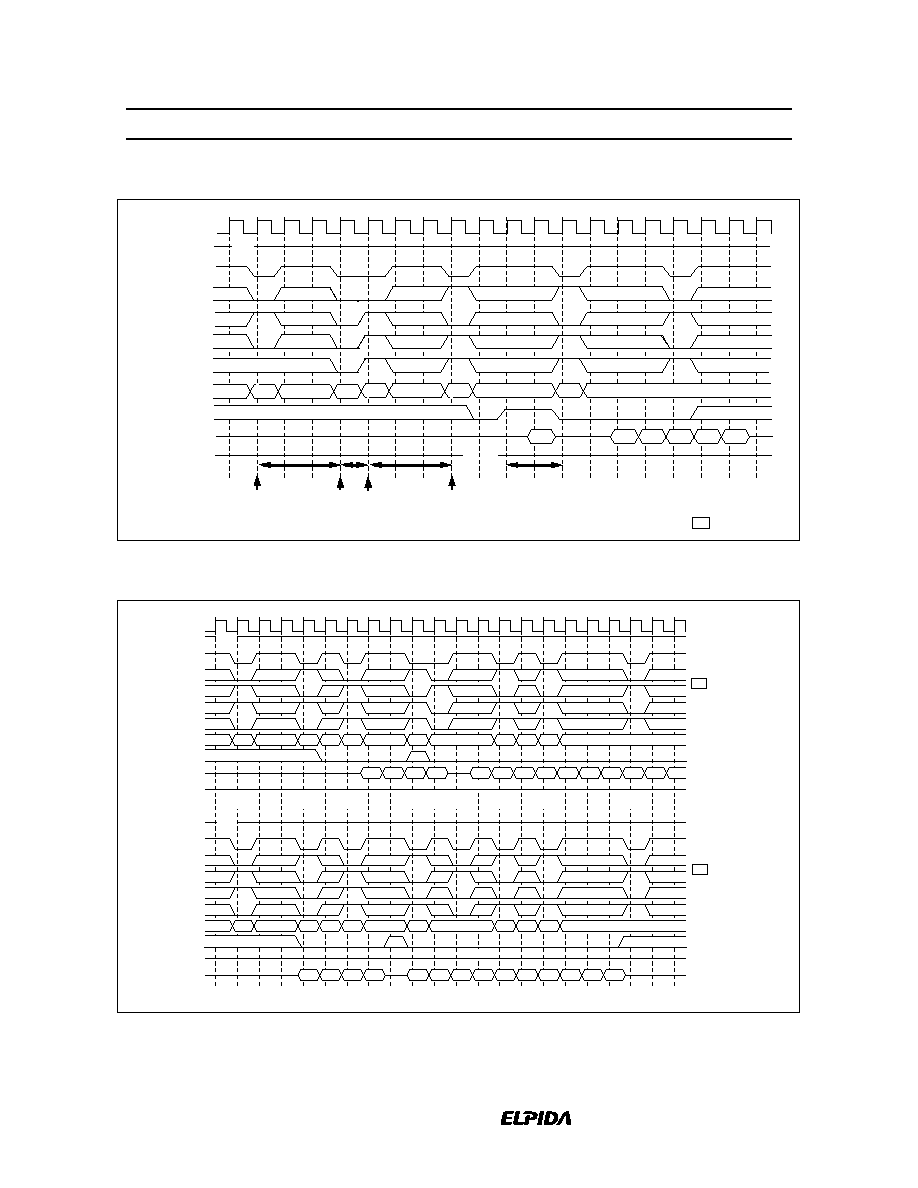
HM5259165B/HM5259805B/HM5259405B-75/A6
Data Sheet E0118H10
56
Mode Register Set Cycle
;
;
0
1
2
3
4
5
6
7
8
9
10
11
12
13
14
15
16
17
18
CLK
CKE
CS
RAS
CAS
WE
BS
Address
DQM,
DQMU/DQML
DQ (input)
DQ (output)
;
;
;;
;;
;
;
;
;
;
;
;;
;
;
;
;
;;
;;
;;
;
;
;
;
;
;;
;
;
;
;;
;
;
;
;
High-Z
b
b+3
b'
b'+1
b'+2
b'+3
l
valid
C: b'
RSA
code
l RCD
l RP
Precharge
If needed
Mode
register
Set
Bank 3
Active
Bank 3
Read
;;
;
;
;
;
;
;
;
;
;
;
;
;
;;
;
;
;
;
;
;
;
;
;;
;
;
;;
;
;
;;
;
;;
;;
;
;
;
;
;
;;
;
;;
;
R: b
C: b
;;
;;
;
;;
;
;
;
;
;;
;
Output mask
V
IH
l = 3
CAS latency = 3
Burst length = 4
= V or V
;;
IH
IL
RCD
Read Cycle/Write Cycle
0
1
2
3
4
5
6
7
8
9
10
11
12
13
14
15
16
17
18
19
20
;
;
;;
;
;
R:a
C:a
R:b
C:b
C:b'
C:b"
a
a+1 a+2 a+3
b
b+1 b+2 b+3 b'
b'+1 b"
b"+1 b"+2 b"+3
CKE
RAS
CS
CAS
WE
Address
DQM,
DQMU/DQML
DQ (output)
DQ (input)
CLK
BS
;
;
;;
;
;
;
;
;
;
;
;
;;
;
;;
;
;
;
;
;
;
;
;
;
;
;
R:a
C:a
R:b
C:b
C:b'
C:b"
;
;
;
;;
a
a+1 a+2 a+3
b
b+1 b+2 b+3 b'
b'+1 b"
b"+1 b"+2 b"+3
;
;
;
;
;;
;
;
;
;
;
;
;
;
;
;
;
;
;
;
;
;
;
;
;
;
;
;
;
;
;
;
;
;
;
;
;
;
;
;
;
;
;
;
;;
;
;
;
;
;
;
;;
;
;
;
;
;
;;
;;
;;
;;
;
;
;
;
;
;
;
;
;
;
;
;
;
;
;
;
;
;
;
;
;
;
;
;
;
;
;
;
;
;
;
;
;
;
;
;
Bank 0
Active
Bank 0
Read
Bank 3
Active
Bank 3
Read
Bank 3
Read
Bank 3
Read
Bank 0
Precharge
Bank 3
Precharge
Bank 0
Active
Bank 0
Write
Bank 3
Active
Bank 3
Write
Bank 3
Write
Bank 3
Write
Bank 0
Precharge
Bank 3
Precharge
CKE
RAS
CS
CAS
WE
Address
DQM,
DQMU/DQML
DQ (input)
DQ (output)
BS
High-Z
High-Z
;
;
;;
;
;
;
;
V
IH
V
IH
Read cycle
RAS-CAS delay = 3
CAS latency = 3
Burst length = 4
= V or V
;;
IH
IL
Write cycle
RAS-CAS delay = 3
CAS latency = 3
Burst length = 4
= V or V
;
IH
IL
HM5259165B/HM5259805B/HM5259405B-75/A6
Data Sheet E0118H10
57
Read/Single Write Cycle
;
;
;
;
;
;
;
;
;
;
;
0
1
2
3
4
5
6
7
8
9
10
11
12
13
14
15
16
17
18
19
20
;
;
;
;
;
;
;
;
;
R:a
C:a
R:b
C:a'
;
;
;
;
;
;
;
;
;
;
;;
;
;
;
R:a
C:a
C:a
;;
;
;
;
;
;
;
;
;
a
a
a
a
;
;
;
;
;
;
;
;
;
;
;
;
;
;
;
;
;
;
;
;;
;
;
;
;
Bank 0
Active
Bank 0
Read
Bank 3
Active
Bank 0
Write
Bank 0
Precharge
Bank 3
Precharge
Bank 0
Active
Bank 0
Read
Bank 0
Write
Bank 0
Precharge
;
;
;
;
;
;
;
;
R:b
Bank 3
Active
;
;;
;;
;
;
;
;
;
;
;
;
;
;
;;
;
;;
;
;
;
;
;
;
;
C:a
Bank 0
Read
a
a+1 a+2 a+3
;
;
;
;
;
;
;
;
;
;
;
;
Bank 0
Write
Bank 0
Write
CKE
RAS
CS
CAS
WE
Address
DQM,
DQMU/DQML
DQ (input)
DQ (output)
CLK
BS
CKE
RAS
CS
CAS
WE
Address
DQM,
DQMU/DQML
BS
;
;
;
;
;
;
C:b
b
c
a+1
a+3
a+1 a+2 a+3
C:c
;
;
;
;
;
;
;
;;
;;
;
;
;
V
IH
V
IH
Read/Single write
RAS-CAS delay = 3
CAS latency = 3
Burst length = 4
= V or V
;
IH
IL
DQ (input)
DQ (output)
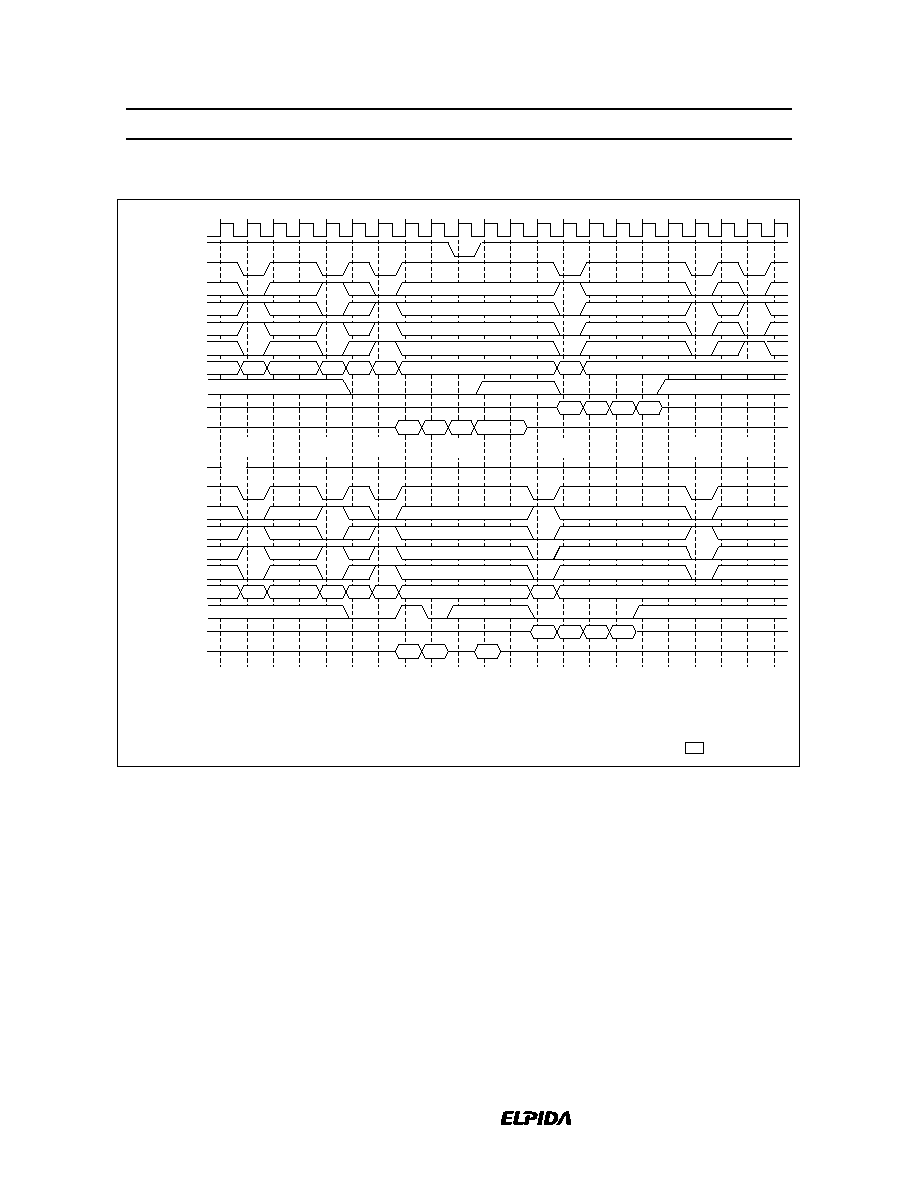
HM5259165B/HM5259805B/HM5259405B-75/A6
Data Sheet E0118H10
58
Read/Burst Write Cycle
;
;
;
;
;
;
;
;
;
;
;
;
;
;
;
;
;
;
;
;
;
;;
0
1
2
3
4
5
6
7
8
9
10
11
12
13
14
15
16
17
18
19
20
;;
;
;
;
;
;
;
;
R:a
C:a
R:b
C:a'
;
;
;
;
;
;
;
;
;
;
;
R:a
C:a
C:a
;
;
;
;
;
;;
;;
;
;
;
;
;
a
a+1 a+2 a+3
a+1
a
a+1 a+2 a+3
;
;
;
;
;
;
;
;
;;
;
;
;
;
;
;
;
;
;
;
;
;
Bank 0
Active
Bank 0
Read
Bank 0
Write
Bank 0
Precharge
;
;
;
;
;
;
;
;
;
;
R:b
Bank 3
Active
;
;
;
;
;
;
;
;
;
;
;
;;
;;
;;
;;
;
;;
;
;;
;
CKE
RAS
CS
CAS
WE
Address
DQM,
DQMU/DQML
CLK
BS
CKE
RAS
CS
CAS
WE
Address
DQM,
DQMU/DQML
BS
a+1 a+2 a+3
a
a+3
a
;
;
;
;
;
;
;
Bank 0
Active
Bank 0
Read
Bank 3
Active
Clock
suspend
Bank 0
Write
Bank 0
Precharge
Bank 3
Precharge
;
;;
V
IH
Read/Burst write
RAS-CAS delay = 3
CAS latency = 3
Burst length = 4
= V or V
;
IH
IL
DQ (input)
DQ (output)
DQ (input)
DQ (output)
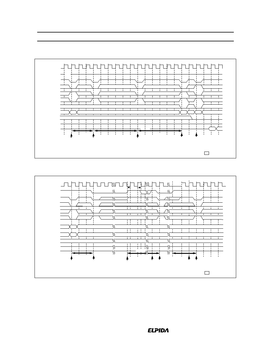
HM5259165B/HM5259805B/HM5259405B-75/A6
Data Sheet E0118H10
59
Auto Refresh Cycle
0
1
2
3
4
5
6
7
8
9
10
11
12
13
14
15
16
17
18
19
20
CLK
CKE
CS
CAS
WE
BS
Address
DQM,
DQMU/DQML
DQ (input)
DQ (output)
;
;;
;
;;
;
;;
;
;
;
;
;
;
;
;
;
;
;;
;
;
;;
;;
;;
;
High-Z
RP
;
;
;
;
;
;
;
;
;
;
;;
;
;
;
;
;
;
;
;
;
Precharge
If needed
Auto Refresh
Active
Bank 0
t
RC
t
RC
t
Auto Refresh
Read
Bank 0
;
;;
;
;;
;;
;
R:a
C:a
A10=1
RAS
;
;
;;
;
;;
;
;
;;
;
;
;
;
;;
;
;
;;
;;
;;
;;
;
;
;
;;
;
;;
;
;;
;
a
a+1
V
IH
Refresh cycle and
Read cycle
RAS-CAS delay = 2
CAS latency = 2
Burst length = 4
= V or V
;
IH
IL
Self Refresh Cycle
;
CLK
CKE
CS
RAS
CAS
WE
BS
Address
DQM,
DQMU/DQML
DQ (input)
DQ (output)
;
;;
;
;;
;
;;
;;
;
;
;
;
;
;
;
;;
;
;
;
;
;
;
;;
;
;;
;
;
;
;;
;
Precharge command
If needed
Self refresh entry
command
Auto
refresh
Self refresh exit
ignore command
or No operation
;
;;
;
;
;
;
;
;
;
;
;
;
;;
;
;
;
CKE Low
;
;;
A10=1
RC
t
RP
t
;
;;
;
;;
;
Self refresh cycle
RAS-CAS delay = 3
CAS latency = 3
Burst length = 4
= V or V
;
IH
IL
;
High-Z
Next
clock
enable
;;
;
;
RC
t
Next
clock
enable
;;
;
l
SREX
Self refresh entry
command
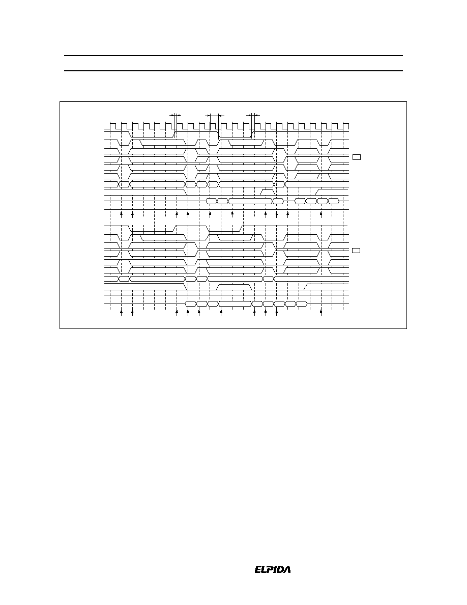
HM5259165B/HM5259805B/HM5259405B-75/A6
Data Sheet E0118H10
60
Clock Suspend Mode
;
;
;
;
;
;
;
;
;
;
;
;
;
;
;
;
;
;;
0
1
2
3
4
5
6
7
8
9
10
11
12
13
14
15
16
17
18
19
20
;
;
;
;
;
;;
;;
;
;
;
;
;
;
;
;
;
R:a
C:a
R:b
a
a+1 a+2
a+3
b
b+1 b+2
;
;
;
;
;
;
;
;
;
;
;
;
;
;
;
;
;
;
;
;
;
R:a
C:a R:b
C:b
;
;;
;;
;
;;
;;
;
;
a
a+1 a+2
b
b+1 b+2 b+3
;
;
;
;
;
;
;
;
;
;;
;;
;
;
;
;
C:b
;
;
;
;
;
;
Bank0
Active
Active clock
suspend start
Active clock
supend end
Bank0
Read
Bank3
Active
Read suspend
start
Read suspend
end
Bank0
Precharge
Bank3
Read
Earliest Bank3
Precharge
Bank0
Write
Bank0
Active
Active clock
suspend start
Active clock
suspend end
Bank3
Active
Write suspend
start
Write suspend
end
Bank3
Write
Bank0
Precharge
Earliest Bank3
Precharge
;
;
;
;
;
;
;;
;;
;
;;
;
;
;
;
;
;
b+3
;
;
;
;
;
;
;
;
;
;
;
;
;
;
;
;
;
;
;
;
;
;
;
CKE
RAS
CS
CAS
WE
Address
DQM,
DQMU/DQML
CLK
BS
CKE
RAS
CS
CAS
WE
Address
DQM,
DQMU/DQML
BS
a+3
High-Z
High-Z
;;
;
;
;
;;
;
;;
;
;
;
;
;;
;
;;
;
;
;
t
CES
t
CEH
t
CES
Read cycle
RAS-CAS delay = 2
CAS latency = 2
Burst length = 4
= V or V
;
IH
IL
Write cycle
RAS-CAS delay = 2
CAS latency = 2
Burst length = 4
= V or V
;;
IH
IL
;
DQ (output)
DQ (input)
DQ (output)
DQ (input)
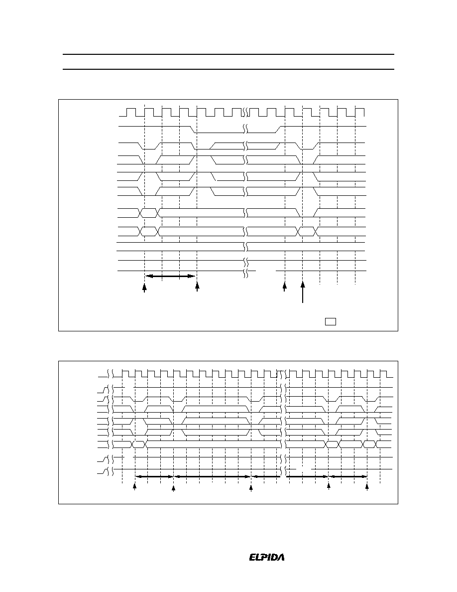
HM5259165B/HM5259805B/HM5259405B-75/A6
Data Sheet E0118H10
61
Power Down Mode
CLK
CKE
CS
RAS
CAS
WE
BS
Address
DQM,
DQMU/DQML
DQ (input)
DQ (output)
;;
;
;
;
;
;
;
;;
;;
;
;;
;;
;
;;
;
;
;;
;
;;
;
;;
;;
;;
;
;
;
;
;
;;
;;
;
;;
;
;
;
Precharge command
If needed
Power down entry
Active Bank 0
Power down
mode exit
;
;
;
;
;
;
;
;
;
;
;
;
CKE Low
R: a
;;
;
;;
A10=1
RP
t
;;
;;
;;
;
High-Z
;
Power down cycle
RAS-CAS delay = 3
CAS latency = 3
Burst length = 4
= V or V
;
IH
IL
Initialization Sequence
7
8
9
10
52
53
54
48
49
50
51
;
;
;
;
Auto Refresh
Bank active
If needed
RC
t
RC
t
Auto Refresh
;
Valid
;
;
0
1
2
3
4
5
6
CLK
CKE
CS
RAS
CAS
WE
Address
DQM,
DQMU/DQML
DQ
;
;
;
;
;
;
t
valid
RSA
t RP
All banks
Precharge
Mode register
Set
;
;
;
;;
;
;
V
IH
V
IH
;
;
;
;
55
High-Z
;
;;
;
;;
;
;;
;
;
;
;;
;
;
;
;;
;
;
;
;
;
;
;;
code
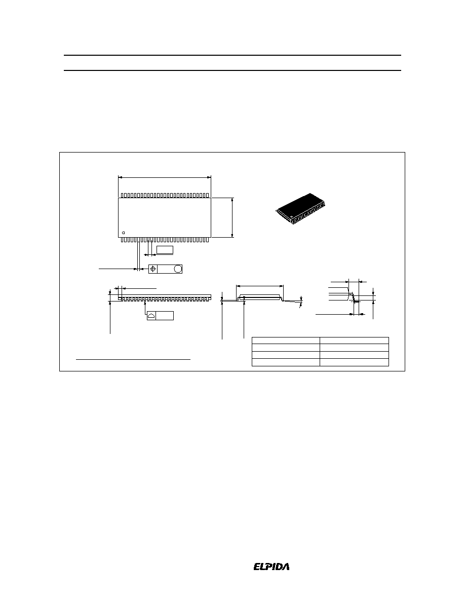
HM5259165B/HM5259805B/HM5259405B-75/A6
Data Sheet E0118H10
62
Package Dimensions
HM5259165BTD
HM5259805BTD
HM5259405BTD Series (TTP-54DA)
Hitachi Code
JEDEC
EIAJ
Weight (reference value)
TTP-54DA
--
--
0.58 g
Unit: mm
*Dimension including the plating thickness
Base material dimension
0.13
M
0.10
0.80
54
28
1
27
22.22
22.72 Max
1.20 Max
10.16
0.05
±
0.05
11.76
± 0.20
0
∞ ≠ 5∞
0.91 Max
*0.12
±
0.05
0.28
± 0.05
0.10
±
0.04
*0.30
0.50
± 0.10
0.45
0.80
+ 0.10
≠ 0.05
HM5259165B/HM5259805B/HM5259405B-75/A6
Data Sheet E0118H10
63
Cautions
1. Elpida Memory, Inc. neither warrants nor grants licenses of any rights of Elpida Memory, Inc.'s or any
third party's patent, copyright, trademark, or other intellectual property rights for information contained in
this document. Elpida Memory, Inc. bears no responsibility for problems that may arise with third party's
rights, including intellectual property rights, in connection with use of the information contained in this
document.
2. Products and product specifications may be subject to change without notice. Confirm that you have
received the latest product standards or specifications before final design, purchase or use.
3. Elpida Memory, Inc. makes every attempt to ensure that its products are of high quality and reliability.
However, contact Elpida Memory, Inc. before using the product in an application that demands especially
high quality and reliability or where its failure or malfunction may directly threaten human life or cause
risk of bodily injury, such as aerospace, aeronautics, nuclear power, combustion control, transportation,
traffic, safety equipment or medical equipment for life support.
4. Design your application so that the product is used within the ranges guaranteed by Elpida Memory, Inc.
particularly for maximum rating, operating supply voltage range, heat radiation characteristics, installation
conditions and other characteristics. Elpida Memory, Inc. bears no responsibility for failure or damage
when used beyond the guaranteed ranges. Even within the guaranteed ranges, consider normally
foreseeable failure rates or failure modes in semiconductor devices and employ systemic measures such as
fail-safes, so that the equipment incorporating Elpida Memory, Inc. product does not cause bodily injury,
fire or other consequential damage due to operation of the Elpida Memory, Inc. product.
5. This product is not designed to be radiation resistant.
6. No one is permitted to reproduce or duplicate, in any form, the whole or part of this document without
written approval from Elpida Memory, Inc..
7. Contact Elpida Memory, Inc. for any questions regarding this document or Elpida Memory, Inc.
semiconductor products.