Document Outline
- COVER
- ˛ˇ
- ˛ˇ
- ˛ˇ
- ˛ˇ
- Pin Description (HM5425161B)
- Pin Arrangement (HM5425801B)
- Pin Description (HM5425801B)
- ˛ˇ
- Pin Description (HM5425401B)
- ˛ˇ
- ˛ˇ
- ˛ˇ
- ˛ˇ
- ˛ˇ
- ˛ˇ
- ˛ˇ
- ˛ˇ
- Data Driver Output Characteristics Curves
- ˛ˇ
- DC Characteristics 2
- ˛ˇ
- ˛ˇ
- ˛ˇ
- ˛ˇ
- ˛ˇ
- ˛ˇ
- ˛ˇ
- ˛ˇ
- ˛ˇ
- ˛ˇ
- ˛ˇ
- ˛ˇ
- ˛ˇ
- ˛ˇ
- ˛ˇ
Elpida Memory, Inc. is a joint venture DRAM company of NEC Corporation and Hitachi, Ltd.
HM5425161B Series
HM5425801B Series
HM5425401B Series
256M SSTL_2 interface DDR SDRAM
143 MHz/133 MHz/125 MHz/100 MHz
4-Mword
◊
16-bit
◊
4-bank/8-Mword
◊
8-bit
◊
4-bank/
16-Mword
◊
4-bit
◊
4-bank
E0086H20 (Ver. 2.0)
Jan. 23, 2002
Description
The HM5425161B, the HM5425801B and the HM5425401B are the Double Data Rate (DDR) SDRAM
devices. Read and write operations are performed at the cross points of the CLK and the
CLK. This high
speed data transfer is realized by the 2-bit prefetch piplined architecture. Data strobe (DQS) both for read and
write are available for high speed and reliable data bus design. By setting extended mode resistor, the on-chip
Delay Locked Loop (DLL) can be set enable or disable.
Features
∑
2.5 V power supply
∑
SSTL-2 interface for all inputs and outputs
∑
Clock frequency: 143 MHz/133 MHz/125 MHz/100 MHz (max)
∑
Data inputs, outputs, and DM are synchronized with DQS
∑
4 banks can operate simultaneously and independently
∑
Burst read/write operation
∑
Programmable burst length: 2/4/8
Burst read stop capability

HM5425161B, HM5425801B, HM5425401B Series
Data Sheet E0086H20
2
∑
Programmable burst sequence
Sequential
Interleave
∑
Start addressing capability
Even and Odd
∑
Programmable
CAS latency: 2/2.5
∑
8192 refresh cycles: 7.8
µ
s (64 ms/8192 cycles)
∑
2 variations of refresh
Auto refresh
Self refresh
Ordering Information
Type No.
Frequency
CAS
latency
Package
HM5425161BTT-75A*
1
HM5425161BTT-75B*
2
HM5425161BTT-10*
3
133 MHz
133 MHz
100 MHz
2.0
2.5
2.0
400-mill 66-pin plastic
TSOP II
HM5425801BTT-75A*
1
HM5425801BTT-75B*
2
HM5425801BTT-10*
3
133 MHz
133 MHz
100 MHz
2.0
2.5
2.0
HM5425401BTT-75A*
1
HM5425401BTT-75B*
2
HM5425401BTT-10*
3
133 MHz
133 MHz
100 MHz
2.0
2.5
2.0
Notes: 1. 143 MHz operation at
CAS
latency = 2.5.
2. 100 MHz operation at
CAS
latency = 2.0.
3. 125 MHz operation at
CAS
latency = 2.5.

HM5425161B, HM5425801B, HM5425401B Series
Data Sheet E0086H20
3
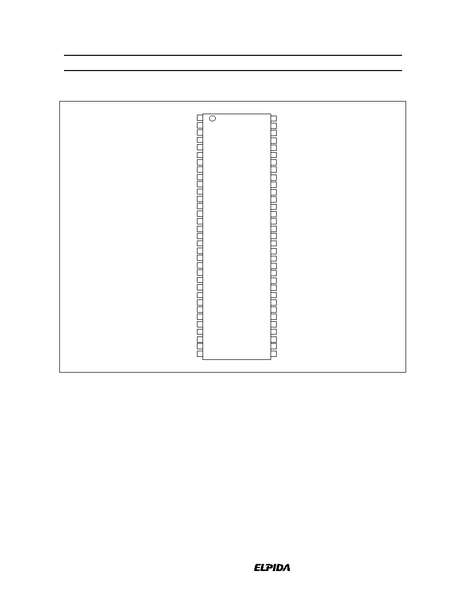
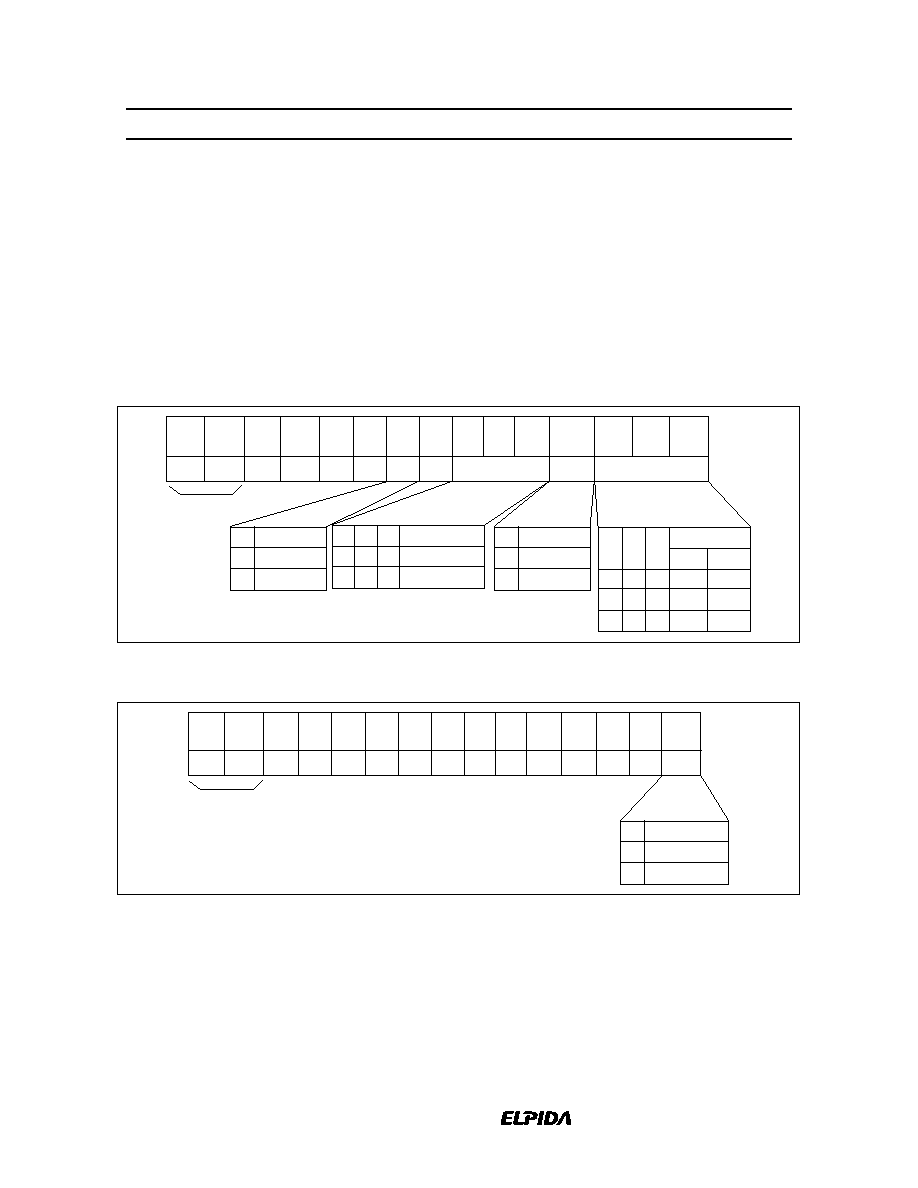
Pin Arrangement (HM5425161B)
1
2
3
4
5
6
7
8
9
10
11
12
13
14
15
16
17
18
19
20
21
22
23
24
25
26
27
28
29
30
31
32
33
V
CC
DQ0
V
CCQ
DQ1
DQ2
V
SSQ
DQ3
DQ4
V
CCQ
DQ5
DQ6
V
SSQ
DQ7
NC
V
CCQ
DQSL
NC
V
CC
NC
DML
WE
CAS
RAS
CS
NC
BA0
BA1
A10(AP)
A0
A1
A2
A3
V
CC
V
SS
DQ15
V
SSQ
DQ14
DQ13
V
CCQ
DQ12
DQ11
V
SSQ
DQ10
DQ9
V
CCQ
DQ8
NC
V
SSQ
DQSU
NC
V
REF
V
SS
DMU
CLK
CLK
CKE
NC
A12
A11
A9
A8
A7
A6
A5
A4
V
SS
66
65
64
63
62
61
60
59
58
57
56
55
54
53
52
51
50
49
48
47
46
45
44
43
42
41
40
39
38
37
36
35
34
66-pin TSOP
(Top view)

HM5425161B, HM5425801B, HM5425401B Series
Data Sheet E0086H20
4
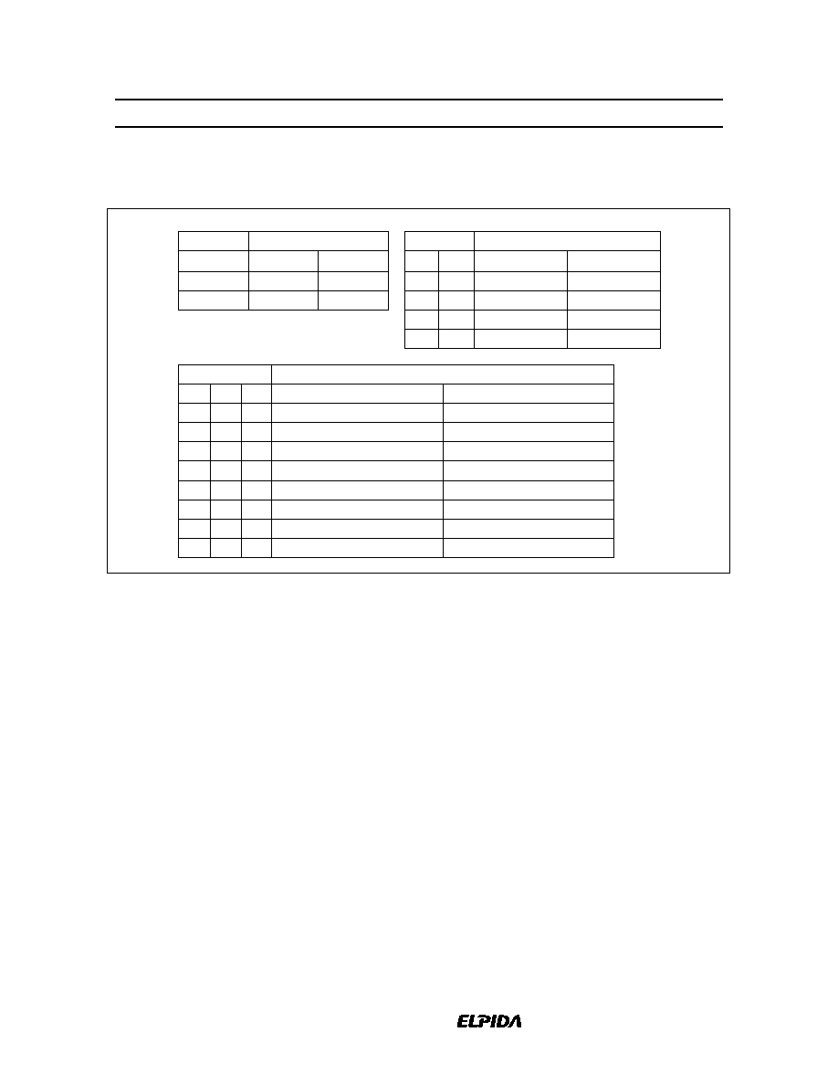
Pin Description
Pin name
Function
A0 to A12
Address input
Row address
A0 to A12
Column address
A0 to A8
BA0, BA1
Bank select address
DQ0 to DQ15
Data-input/output
DQSU
Upper input and output data strobe
DQSL
Lower input and output data strobe
CS
Chip select
RAS
Row address strobe command
CAS
Column address strobe command
WE
Write enable
DMU
Upper byte input mask
DML
Lower byte input mask
CLK
Clock input
CLK
Differential clock input
CKE
Clock enable
V
REF
Input reference voltage
V
CC
Power for internal circuit
V
SS
Ground for internal circuit
V
CCQ
Power for DQ circuit
V
SSQ
Ground for DQ circuit
NC
No connection
HM5425161B, HM5425801B, HM5425401B Series
Data Sheet E0086H20
5
Pin Arrangement (HM5425801B)
1
2
3
4
5
6
7
8
9
10
11
12
13
14
15
16
17
18
19
20
21
22
23
24
25
26
27
28
29
30
31
32
33
V
CC
DQ0
V
CCQ
NC
DQ1
V
SSQ
NC
DQ2
V
CCQ
NC
DQ3
V
SSQ
NC
NC
V
CCQ
NC
NC
V
CC
NC
NC
WE
CAS
RAS
CS
NC
BA0
BA1
A10(AP)
A0
A1
A2
A3
V
CC
V
SS
DQ7
V
SSQ
NC
DQ6
V
CCQ
NC
DQ5
V
SSQ
NC
DQ4
V
CCQ
NC
NC
V
SSQ
DQS
NC
V
REF
V
SS
DM
CLK
CLK
CKE
NC
A12
A11
A9
A8
A7
A6
A5
A4
V
SS
66
65
64
63
62
61
60
59
58
57
56
55
54
53
52
51
50
49
48
47
46
45
44
43
42
41
40
39
38
37
36
35
34
66-pin TSOP
(Top view)

HM5425161B, HM5425801B, HM5425401B Series
Data Sheet E0086H20
6
Pin Description
Pin name
Function
A0 to A12
Address input
Row address
A0 to A12
Column address
A0 to A9
BA0, BA1
Bank select address
DQ0 to DQ7
Data-input/output
DQS
Input and output data strobe
CS
Chip select
RAS
Row address strobe command
CAS
Column address strobe command
WE
Write enable
DM
Input mask
CLK
Clock input
CLK
Differential clock input
CKE
Clock enable
V
REF
Input reference voltage
V
CC
Power for internal circuit
V
SS
Ground for internal circuit
V
CCQ
Power for DQ circuit
V
SSQ
Ground for DQ circuit
NC
No connection

HM5425161B, HM5425801B, HM5425401B Series
Data Sheet E0086H20
7
Pin Arrangement (HM5425401B)
1
2
3
4
5
6
7
8
9
10
11
12
13
14
15
16
17
18
19
20
21
22
23
24
25
26
27
28
29
30
31
32
33
V
CC
NC
V
CCQ
NC
DQ0
V
SSQ
NC
NC
V
CCQ
NC
DQ1
V
SSQ
NC
NC
V
CCQ
NC
NC
V
CC
NC
NC
WE
CAS
RAS
CS
NC
BA0
BA1
A10(AP)
A0
A1
A2
A3
V
CC
V
SS
NC
V
SSQ
NC
DQ3
V
CCQ
NC
NC
V
SSQ
NC
DQ2
V
CCQ
NC
NC
V
SSQ
DQS
NC
V
REF
V
SS
DM
CLK
CLK
CKE
NC
A12
A11
A9
A8
A7
A6
A5
A4
V
SS
66
65
64
63
62
61
60
59
58
57
56
55
54
53
52
51
50
49
48
47
46
45
44
43
42
41
40
39
38
37
36
35
34
66-pin TSOP
(Top view)

HM5425161B, HM5425801B, HM5425401B Series
Data Sheet E0086H20
8
Pin Description
Pin name
Function
A0 to A12
Address input
Row address
A0 to A12
Column address
A0 to A9, A11
BA0, BA1
Bank select address
DQ0 to DQ3
Data-input/output
DQS
Output data strobe
CS
Chip select
RAS
Row address strobe command
CAS
Column address strobe command
WE
Write enable
DM
Input mask
CLK
Clock input
CLK
Differential clock input
CKE
Clock enable
V
REF
Input reference voltage
V
CC
Power for internal circuit
V
SS
Ground for internal circuit
V
CCQ
Power for DQ circuit
V
SSQ
Ground for DQ circuit
NC
No connection
HM5425161B, HM5425801B, HM5425401B Series
Data Sheet E0086H20
9
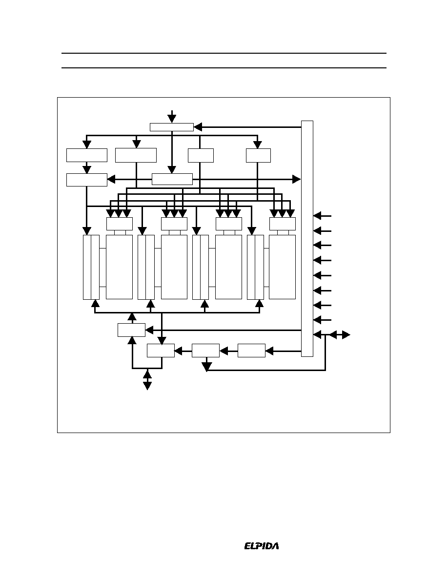
Block Diagram
Column address
counter
Column address
buffer
Row address
buffer
Bank
select
Refresh
counter
Address register
Address (A12, BA0, BA1)
AY0 to AY11
AX0 to AX12
BA0, BA1
A0 to A12,
BA0, BA1
DQ*
2
Input
buffer
Output
buffer
DQS
buffer
Row
decoder
Sense amplifier & I/O bus
Column decoder
Bank 0
*
1
*
1
*
1
*
1
Notes: 1. 8192 row
◊
512 column
◊
16 bit: HM5425161B
8192 row
◊
1024 column
◊
8 bit: HM5425801B
8192 row
◊
2048 column
◊
4 bit: HM5425401B
2. DQ0 to DQ15: HM5425161B
DQ0 to DQ7: HM5425801B
DQ0 to DQ3: HM5425401B
Row
decoder
Sense amplifier & I/O bus
Column decoder
Bank 1
Row
decoder
Sense amplifier & I/O bus
Column decoder
Bank 2
Row
decoder
CLK
CKE
DM,
DMU/DML
DLL
DQS,
DQSU/DQSL
CLK
RAS
CAS
WE
CS
Sense amplifier & I/O bus
Column decoder
Bank 3
Control logic & timing generator
Mode register

HM5425161B, HM5425801B, HM5425401B Series
Data Sheet E0086H20
10
Pin Functions (1)
CLK,
CLK (input pin): The CLK and the CLK are the master clock inputs. All inputs except DMs, DQSs
and DQs are referred to the cross point of the CLK rising edge and the V
REF
level. When a read operation,
DQSs and DQs are referred to the cross point of the CLK and the
CLK. When a write operation, DMs and
DQs are referred to the cross point of the DQS and the V
REF
level. DQSs for write operation are referred to
the cross point of the CLK and the
CLK.
CS (input pin): When CS is Low, commands and data can be input. When CS is High, all inputs are
ignored. However, internal operations (bank active, burst operations, etc.) are held.
RAS, CAS, and WE (input pins): These pins define operating commands (read, write, etc.) depending on
the combinations of their voltage levels. See "Command operation".
A0 to A12 (input pins): Row address (AX0 to AX12) is determined by the A0 to the A12 level at the cross
point of the CLK rising edge and the V
REF
level in a bank active command cycle. Column address (AY0 to
AY8; the HM5425161B, AY0 to AY9; the HM5425801B, AY0 to AY9, AY11; the HM5425401B) is loaded
via the A0 to the A9 at the cross point of the CLK rising edge and the V
REF
level in a read or a write command
cycle. This column address becomes the starting address of a burst operation.
A10 (AP) (input pin): A10 defines the precharge mode when a precharge command, a read command or a
write command is issued. If A10 = High when a precharge command is issued, all banks are precharged. If
A10 = Low when a precharge command is issued, only the bank that is selected by BA1/BA0 is precharged.
If A10 = High when read or write command, auto-precharge function is enabled. While A10 = Low, auto-
precharge function is disabled.
BA0/BA1 (input pin): BA0/BA1 are bank select signals. The memory array is divided into bank 0, bank 1,
bank 2 and bank 3. If BA1 = Low and BA0 = Low, bank 0 is selected. If BA1 = High and BA0 = Low, bank
1 is selected. If BA1 = Low and BA0 = High, bank 2 is selected. If BA1 = High and BA0 = High, bank 3 is
selected.
CKE (input pin): CKE controls power down and self-refresh. The power down and the self-refresh
commands are entered when the CKE is driven Low and exited when it resumes to High.
The CKE level must be kept for 1 CLK cycle (= t
CKEPW
) at least, that is, if CKE changes at the cross point of
the CLK rising edge and the V
REF
level with proper setup time t
IS
, by the next CLK rising edge CKE level
must be kept with proper hold time t
IH
.

HM5425161B, HM5425801B, HM5425401B Series
Data Sheet E0086H20
11
Pin Functions (2)
DM, DMU/DML (input pins): DM (the HM5425801B and the HM5425401B), DMU/DML (the
HM5425161B) are the reference signals of the data input mask function. DMs are sampled at the cross point
of DQS and V
REF
. DMU/DML provide the byte mask function. When DMU/DML = High, the data input at
the same timing are masked while the internal burst counter will be count up. DML controls the lower byte
(DQ0 to DQ7) and DMU controls the upper byte (DQ8 to DQ15) of write data.
DQ0 to DQ15 (input and output pins): Data are input to and output from these pins (the DQ0 to the DQ15;
the HM5425161B, the DQ0 to the DQ7; the HM5425801B, the DQ0 to the DQ3; the HM5425401B).
DQS, DQSU/DQSL (input and output pin):
DQS (the HM5425801B and the HM5425401B),
DQSU/DQSL (the HM5425161B) provide the read data strobes (as output) and the write data strobes (as
input). DQSL is the lower byte (DQ0 to DQ7) data strobe signal, DQSU is the upper byte (DQ8 to DQ15)
data strobe signal.
V
CC
and V
CCQ
(power supply pins): 2.5 V is applied. (V
CC
is for the internal circuit and V
CCQ
is for the
output buffer.)
V
SS
and V
SSQ
(power supply pins): Ground is connected. (V
SS
is for the internal circuit and V
SSQ
is for the
output buffer.)
HM5425161B, HM5425801B, HM5425401B Series
Data Sheet E0086H20
12
Command Operation
Command Truth Table
The HM5425161B, the HM5425801B and HM5425401B recognize the following commands specified by the
CS, RAS, CAS, WE and address pins. All other combinations than those in the table below are illegal.
CKE
Command
Symbol
n ≠ 1 n
CS
RAS CAS WE
BA1 BA0 AP
Address
Ignore command
DESL
H
H
H
◊
◊
◊
◊
◊
◊
◊
No operation
NOP
H
H
L
H
H
H
◊
◊
◊
◊
Burst stop in read command
BST
H
H
L
H
H
L
◊
◊
◊
◊
Column address and read command
READ
H
H
L
H
L
H
V
V
L
V
Read with auto-precharge
READA
H
H
L
H
L
H
V
V
H
V
Column address and write command
WRIT
H
H
L
H
L
L
V
V
L
V
Write with auto-precharge
WRITA
H
H
L
H
L
L
V
V
H
V
Row address strobe and bank active
ACTV
H
H
L
L
H
H
V
V
V
V
Precharge select bank
PRE
H
H
L
L
H
L
V
V
L
◊
Precharge all bank
PALL
H
H
L
L
H
L
◊
◊
H
◊
Refresh
REF
H
H
L
L
L
H
◊
◊
◊
◊
SELF
H
L
L
L
L
H
◊
◊
◊
◊
Mode register set
MRS
H
H
L
L
L
L
L
L
L
V
EMRS
H
H
L
L
L
L
L
H
L
V
Notes: 1. H: V
IH
. L: V
IL
.
◊
: V
IH
or V
IL
. V: Valid address input
2. The CKE level must be kept for 1 CLK cycle (= t
CKEPW
) at least.
Ignore command [DESL]: When
CS is High at the cross point of the CLK rising edge and the V
REF
level,
every input are neglected and internal status is held.
No operation [NOP]: As long as this command is input at the cross point of the CLK rising edge and the
V
REF
level, address and data input are neglected and internal status is held.
Burst stop in read operation [BST]: This command stops a burst read operation, which is not applicable for
a burst write operation.
Column address strobe and read command [READ]: This command starts a read operation. The start
address of the burst read is determined by the column address (AY0 to AY8; the HM5425161B, AY0 to AY9;
the HM5425801B, AY0 to AY9, AY11; the HM5425401B) and the bank select address (BA). After the
completion of the read operation, the output buffer becomes High-Z.

HM5425161B, HM5425801B, HM5425401B Series
Data Sheet E0086H20
13
Read with auto-precharge [READA]: This command starts a read operation. After completion of the read
operation, precharge is automatically executed.
Column address strobe and write command [WRIT]: This command starts a write operation. The start
address of the burst write is determined by the column address (AY0 to AY8; the HM5425161B, AY0 to
AY9; the HM5425801B, AY0 to AY9, AY11; the HM5425401B) and the bank select address (BA).
Write with auto-precharge [WRITA]: This command starts a write operation. After completion of the
write operation, precharge is automatically executed.
Row address strobe and bank activate [ACTV]: This command activates the bank selected by BA0/BA1
and determines a row address (AX0 to AX12). When BA1 = BA0 = Low, bank 0 is activated. When BA1 =
High and BA0 = Low, bank 1 is activated. When BA1 = Low and BA0 = High, bank 2 is activated. When
BA1 = BA0 = High, bank 3 is activated.
Precharge selected bank [PRE]: This command starts a pre-charge operation for the bank selected by
BA0/BA1.
Precharge all banks [PALL]: This command starts a precharge operation for all banks.
Refresh [REF/SELF]: This command starts a refresh operation. There are two types of refresh operation,
one is auto-refresh, and another is self-refresh. For details, refer to the CKE truth table section.
Mode register set/Extended mode register set [MRS/EMRS]: The DDR SDRAM has the two mode
registers, the mode register and the extended mode register, to defines how it works. The both mode registers
are set through the address pins (the A0 to the A12, BA0 to BA1) in the mode register set cycle. For details,
refer to "Mode register and extended mode register set".
HM5425161B, HM5425801B, HM5425401B Series
Data Sheet E0086H20
14
CKE Truth Table
CKE
Current state
Command
n ≠ 1
n
CS
RAS CAS WE
Address Notes
Idle
Auto-refresh command (REF)
H
H
L
L
L
H
◊
2
Idle
Self-refresh entry (SELF)
H
L
L
L
L
H
◊
2
Idle
Power down entry (PDEN)
H
L
L
H
H
H
◊
H
L
H
◊
◊
◊
◊
Self refresh
Self refresh exit (SELFX)
L
H
L
H
H
H
◊
L
H
H
◊
◊
◊
◊
Power down
Power down exit (PDEX)
L
H
L
H
H
H
◊
L
H
H
◊
◊
◊
◊
Notes: 1. H: V
IH
. L: V
IL
.
◊
: V
IH
or V
IL
.
2. All the banks must be in IDLE before executing this command.
3. The CKE level must be kept for 1 CLK cycle (= t
CKEPW
) at least.
Auto-refresh command [REF]: This command executes auto-refresh. The banks and the ROW addresses
to be refreshed are internally determined by the internal refresh contoroller. The average refresh cycle is 7.8
µ
s. The output buffer becomes High-Z after auto-refresh start. Precharge has been completed automatically
after the auto-refresh. The ACTV or MRS command can be issued t
RFC
after the last auto-refresh command.
Self-refresh entry [SELF]: This command starts self-refresh. The self-refresh operation continues as long
as CKE is held Low. During the self-refresh operation, all ROW addresses are repeated refreshing by the
internal refresh contoroller. A self-refresh is terminated by a self-refresh exit command.
Power down mode entry [PDEN]: t
PDEN
(= 1 cycle) after the cycle when [PDEN] is issued. The DDR
SDRAM enters into power-down mode. In power down mode, power consumption is suppressed by
deactivating the input initial circuit. Power down mode continues while CKE is held Low. No internal
refresh operation occurs during the power down mode. [PDEN] do not disable DLL.
Self-refresh exit [SELFX]: This command is executed to exit from self-refresh mode. 10 cycles (= t
SNR
)
after [SELFX], non-read commands can be executed. For read operation, wait for 200 cycles (= t
SRD
) after
[SELFX] to adjust Dout timing by DLL. After the exit, within 7.8
µ
s input auto-refresh command.
Power down exit [PDEX]: The DDR SDRAM can exit from power down mode t
PDEX
(1 cycle min.) after the
cycle when [PDEX] is issued.
HM5425161B, HM5425801B, HM5425401B Series
Data Sheet E0086H20
15
Function Truth Table
The following tables show the operations that are performed when each command is issued in each state of
the DDR SDRAM.
Function Truth Table (1)
Current state
CS
RAS CAS WE
Address
Command
Operation
Next state
Precharging*
2
H
◊
◊
◊
◊
DESL
NOP
ldle
L
H
H
H
◊
NOP
NOP
ldle
L
H
H
L
◊
BST
ILLEGAL*
12
--
L
H
L
H
BA, CA, A10
READ/READA
ILLEGAL*
12
--
L
H
L
L
BA, CA, A10
WRIT/WRITA
ILLEGAL*
12
--
L
L
H
H
BA, RA
ACTV
ILLEGAL*
12
--
L
L
H
L
BA, A10
PRE, PALL
NOP
ldle
L
L
L
◊
◊
ILLEGAL
--
Idle*
3
H
◊
◊
◊
◊
DESL
NOP
ldle
L
H
H
H
◊
NOP
NOP
ldle
L
H
H
L
◊
BST
ILLEGAL*
12
--
L
H
L
H
BA, CA, A10
READ/READA
ILLEGAL*
12
--
L
H
L
L
BA, CA, A10
WRIT/WRITA
ILLEGAL*
12
--
L
L
H
H
BA, RA
ACTV
Activating
Active
L
L
H
L
BA, A10
PRE, PALL
NOP
ldle
L
L
L
H
◊
REF, SELF
Refresh/
Selfrefresh*
13
ldle/
Selfrefresh
L
L
L
L
MODE
MRS
Mode register set*
13
ldle
Refresh
(auto-refresh)*
4
H
◊
◊
◊
◊
DESL
NOP
ldle
L
H
H
H
◊
NOP
NOP
ldle
H
H
H
L
◊
BST
ILLEGAL
--
L
H
L
◊
◊
ILLEGAL
--
L
L
◊
◊
◊
ILLEGAL
--
HM5425161B, HM5425801B, HM5425401B Series
Data Sheet E0086H20
16
Function Truth Table (2)
Current state
CS
RAS CAS WE
Address
Command
Operation
Next state
Activating*
5
H
◊
◊
◊
◊
DESL
NOP
Active
L
H
H
H
◊
NOP
NOP
Active
L
H
H
L
◊
BST
ILLEGAL*
12
--
L
H
L
H
BA, CA, A10
READ/READA
ILLEGAL*
12
--
L
H
L
L
BA, CA, A10
WRIT/WRITA
ILLEGAL*
12
--
L
L
H
H
BA, RA
ACTV
ILLEGAL*
12
--
L
L
H
L
BA, A10
PRE, PALL
ILLEGAL*
12
--
L
L
L
◊
◊
ILLEGAL
--
Active*
6
H
◊
◊
◊
◊
DESL
NOP
Active
L
H
H
H
◊
NOP
NOP
Active
L
H
H
L
◊
BST
ILLEGAL
Active
L
H
L
H
BA, CA, A10
READ/READA
Starting read
operation
Read/READ
A
L
H
L
L
BA, CA, A10
WRIT/WRITA
Starting write
operation
Write
recovering/
precharging
L
L
H
H
BA, RA
ACTV
ILLEGAL*
12
--
L
L
H
L
BA, A10
PRE, PALL
Pre-charge
Idle
L
L
L
◊
◊
ILLEGAL
--
Read*
7
H
◊
◊
◊
◊
DESL
NOP
Active
L
H
H
H
◊
NOP
NOP
Active
L
H
H
L
◊
BST
BST
Active
L
H
L
H
BA, CA, A10
READ/READA
Interrupting burst
read operation to
start new read
Active
L
H
L
L
BA, CA, A10
WRIT/WRITA
ILLEGAL*
14
--
L
L
H
H
BA, RA
ACTV
ILLEGAL*
12
--
L
L
H
L
BA, A10
PRE, PALL
Interrupting burst
read operation to
start pre-charge
Precharging
L
L
L
◊
◊
ILLEGAL
--
HM5425161B, HM5425801B, HM5425401B Series
Data Sheet E0086H20
17
Function Truth Table (3)
Current state
CS
RAS CAS WE
Address
Command
Operation
Next state
Read with auto-
pre-charge*
8
H
◊
◊
◊
◊
DESL
NOP
Precharging
L
H
H
H
◊
NOP
NOP
Precharging
L
H
H
L
◊
BST
ILLEGAL*
15
--
L
H
L
H
BA, CA, A10
READ/READA
ILLEGAL*
15
--
L
H
L
L
BA, CA, A10
WRIT/WRITA
ILLEGAL*
15
--
L
L
H
H
BA, RA
ACTV
ILLEGAL*
12, 15
--
L
L
H
L
BA, A10
PRE, PALL
ILLEGAL*
12, 15
--
L
L
L
◊
◊
ILLEGAL
--
Write*
9
H
◊
◊
◊
◊
DESL
NOP
Write
recovering
L
H
H
H
◊
NOP
NOP
Write
recovering
L
H
H
L
◊
BST
ILLEGAL
--
L
H
L
H
BA, CA, A10
READ/READA
Interrupting burst
write operation to
start read operation.
Read/ReadA
L
H
L
L
BA, CA, A10
WRIT/WRITA
Interrupting burst
write operation to
start new write
operation.
Write/WriteA
L
L
H
H
BA, RA
ACTV
ILLEGAL*
12
--
L
L
H
L
BA, A10
PRE, PALL
Interrupting write
operation to start
pre-charge.
Idle
L
L
L
◊
◊
ILLEGAL
--
Write
recovering*
10
H
◊
◊
◊
◊
DESL
NOP
Active
L
H
H
H
◊
NOP
NOP
Active
L
H
H
L
◊
BST
ILLEGAL
--
L
H
L
H
BA, CA, A10
READ/READA
Starting read
operation.
Read/ReadA
L
H
L
L
BA, CA, A10
WRIT/WRITA
Starting new write
operation.
Write/WriteA
L
L
H
H
BA, RA
ACTV
ILLEGAL*
12
--
L
L
H
L
BA, A10
PRE/PALL
ILLEGAL*
12
--
L
L
L
◊
◊
ILLEGAL
--
HM5425161B, HM5425801B, HM5425401B Series
Data Sheet E0086H20
18
Function Truth Table (4)
Current state
CS
RAS CAS WE
Address
Command
Operation
Next state
Write with auto-
pre-charge*
11
H
◊
◊
◊
◊
DESL
NOP
Precharging
L
H
H
H
◊
NOP
NOP
Precharging
L
H
H
L
◊
BST
ILLEGAL
--
L
H
L
H
BA, CA, A10
READ/READA
ILLEGAL*
15
--
L
H
L
L
BA, CA, A10
WRIT/WRIT A
ILLEGAL*
15
--
L
L
H
H
BA, RA
ACTV
ILLEGAL*
12, 15
--
L
L
H
L
BA, A10
PRE, PALL
ILLEGAL*
12, 15
--
L
L
L
◊
◊
ILLEGAL
--
Notes: 1. H: V
IH
. L: V
IL
.
◊
: V
IH
or V
IL
.
2. The DDR SDRAM is in "Precharging" state for t
RP
after precharge command is issued.
3. The DDR SDRAM reachs "IDLE" state t
RP
after precharge command is issued.
4. The DDR SDRAM is in "Refresh" state for t
RC
after auto-refresh command is issued.
5. The DDR SDRAM is in "Activating" state for t
RCD
after ACTV command is issued.
6. The DDR SDRAM is in "Active" state after "Activating" is completed.
7. The DDR SDRAM is in "READ" state until burst data have been output and DQ output circuits are
turned off.
8. The DDR SDRAM is in "READ with auto-precharge" from READA command until burst data has
been output and DQ output circuits are turned off.
9. The DDR SDRAM is in "WRITE" state from WRIT command to the last burst data are input.
10. The DDR SDRAM is in "Write recovering" for t
WR
after the last data are input.
11. The DDR SDRAM is in "Write with auto-precharge" until t
WR
after the last data has been input.
12. This command may be issued for other banks, depending on the state of the banks.
13. All banks must be in "IDLE".
14. Before executing a write command to stop the preceding burst read operation, BST command must
be issued.
15. See `Read with Auto-Precharge Enabled, Write with Auto-Precharge Enable' section.
HM5425161B, HM5425801B, HM5425401B Series
Data Sheet E0086H20
19
Read with Auto-Precharge Enabled, Write with Auto-Precharge Enabled
The Elpida HM5425401/801/161B series support the concurrent auto precharge feature, a read with auto-
precharge enabled, or a write with auto-precharge enabled, may be followed by any command to the other
banks, as long as that command does not interrupt the read or write data transfer, and all other related
limitations apply (e.g. contention between READ data and WRITE data must be avoided.)
The minimum delay from a read or write command with auto precharge enabled, to a command to a
different bank, is summarized below.
From command
To command (different bank, non-
interrupting command)
Minimum delay
(Concurrent AP supported)
Units
Read w/AP
Read or Read w/AP
BL/2
tCK
Write or Write w/AP
CL(rounded up)+ (BL/2)
tCK
Precharge or Activate
1
tCK
Write w/AP
Read or Read w/AP
1 + (BL/2) + tWTR
tCK
Write or Write w/AP
BL/2
tCK
Precharge or Activate
1
tCK
HM5425161B, HM5425801B, HM5425401B Series
Data Sheet E0086H20
20
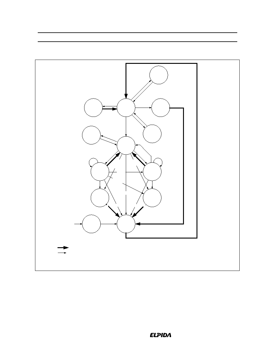
Simplified State Diagram
PRECHARGE
ROW
ACTIVE
IDLE
IDLE
POWER
DOWN
AUTO
REFRESH
SELF
REFRESH
MODE
REGISTER
SET
ACTIVE
POWER
DOWN
POWER
ON
WRITEA
READA
SR ENTRY
SR EXIT
MRS
REFRESH
CKEH
CKEL
CKEH
CKEL
ACTIVE
WRITE
READ
BST
WRITE
WITH AP
READ
WITH AP
POWER
APPLIED
PRECHARGE
AP
READ
WRITE
WITH
AP
READ
WITH
READ
WITH AP
PRECHARGE
PRECHARGE
PRECHARGE
*1
READ
Read
WRITE
Write
Automatic transition after completion of command.
Transition resulting from command input.
Note: 1. After the auto-refresh operation, precharge operation is performed automatically
and enter the IDLE state.
HM5425161B, HM5425801B, HM5425401B Series
Data Sheet E0086H20
21
Operation of the DDR SDRAM
Power-up Sequence
The following sequence is recommended for Power-up.
(1) Apply power and attempt to maintain CKE at an LVCMOS low state (all other inputs may be undefined).
Apply V
CC
before or at the same time as V
CCQ
.
Apply V
CCQ
before or at the same time as V
TT
and V
REF
.
(2) Start clock and maintain stable condition for a minimum of 200 µs.
(3) After the minimum 200 µs of stable power and clock (CLK,
CLK), apply NOP and take CKE high.
(4) Issue precharge all command for the device.
(5) Issue EMRS to enable DLL.
(6) Issue a mode register set command (MRS) for "DLL reset" with bit A8 set to high (An additional 200
cycles of clock input is required to lock the DLL after every DLL reset).
(7) Issue precharge all command for the device.*
1
(8) Issue 2 or more auto-refresh commands.*
1
(9) Issue a mode register set command to initialize device operation with bit A8 set to low in order to avoid
resetting the DLL.
Note: 1. Sequence of (7) and (8) may be reversed.
Power-up Sequence after CKE Goes High
Command
EMRS
PALL
MRS
REF
2 cycles (min)
2 cycles (min)
200 cycles (min)
2 cycles (min)
2 cycles (min)
t
RP
t
RC
t
RC
PALL
MRS
REF
REF
Any
command
DLL enable
DLL reset
with A8 = High
Disable DLL reset
with A8 = Low
(4)
(5)
(6)
(7)
(8)
(9)
HM5425161B, HM5425801B, HM5425401B Series
Data Sheet E0086H20
22
Mode Register and Extended Mode Register Set
There are two mode registers, the mode register and the extended mode register so as to define the operating
mode. Parameters are set to both through the A0 to the A12 and BA0, BA1 pins by the mode register set
command [MRS] or the extended mode register set command [EMRS]. The mode register and the extended
mode register are set by inputting signal via the A0 to the A12 and BA0, BA1 during mode register set cycles.
BA0 and BA1 determine which one of the mode register or the extended mode register are set. Prior to a read
or a write operation, the mode register must be set.
Remind that no other parameters are shown in the table bellow are allowed to input to the registers.
Mode Register Set [MRS] (BA0 = 0, BA1 = 0)
A2 A1 A0
Burst Length
0
0
1
2
0
1
0
4
0
1
1
8
BT=0 BT=1
2
4
8
A3
0
Sequential
1
Interleave
Burst Type
A6 A5 A4 CAS Latency
0
1
0
2
2.5
1
1
0
A9
A8
A7
A6
A5
A4
A3
A2
A1
A0
0
0
0
0
0
DR
LMODE
BT
BL
A8
0
No
1
Yes
DLL Reset
A11
A10
A12
BA1
0
BA0
0
MRS
Extended Mode Register Set [EMRS] (BA0 = 1, BA1 = 0)
A0
0
DLL Enable
1
DLL Disable
DLL Control
A9
A8
A7
A6
A5
A4
A3
A2
A1
A0
0
0
0
0
0
0
0
0
0
0
0
DLL
0
A11 A10
A12
BA1
0
BA0
1
EMRS
HM5425161B, HM5425801B, HM5425401B Series
Data Sheet E0086H20
23
Burst Operation
The burst type (BT) and the first three bits of the column address determines the order of a data out.
A2
A1
A0
Addressing(decimal)
0
0
0
0
0
1
0
1
0
0
1
1
1
1
1
Interleave
Sequence
1
0
0
1
1
0
1
0
1
Starting Ad.
0, 1, 2, 3, 4, 5, 6, 7,
1, 2, 3, 4, 5, 6, 7,
2, 3, 4, 5, 6, 7,
3, 4, 5, 6, 7,
4, 5, 6, 7,
5, 6, 7,
6, 7,
7,
0,
0, 1,
0, 1, 2,
0, 1, 2, 3,
0, 1, 2, 3, 4,
0, 1, 2, 3, 4, 5,
0, 1, 2, 3, 4, 5, 6,
0, 1, 2, 3, 4, 5, 6, 7,
1, 0, 3, 2, 5, 4, 7,
2, 3, 0, 1, 6, 7,
3, 2, 1, 0, 7,
4, 5, 6, 7,
5, 4, 7,
6, 7,
7,
6,
4, 5,
6, 5, 4,
0, 1, 2, 3,
6, 1, 0, 3, 2,
4, 5, 2, 3, 0, 1,
6, 5, 4, 3, 2, 1, 0,
Burst length = 8
A1
A0
Addressing(decimal)
0
0
0
1
1
0
1
1
Interleave
Sequence
Starting Ad.
0, 1, 2, 3,
1, 2, 3, 0,
2, 3, 0, 1,
3, 0, 1, 2,
0, 1, 2, 3,
1, 0, 3, 2,
2, 3, 0, 1,
3, 2, 1, 0,
Burst length = 4
A0
Addressing(decimal)
0
1
Interleave
Sequence
Starting Ad.
0, 1,
1, 0,
0, 1,
1, 0,
Burst length = 2
HM5425161B, HM5425801B, HM5425401B Series
Data Sheet E0086H20
24
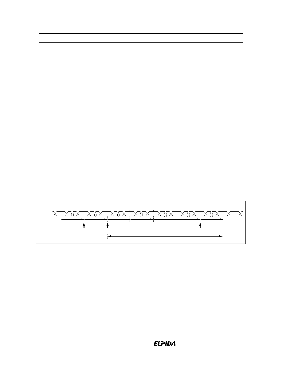
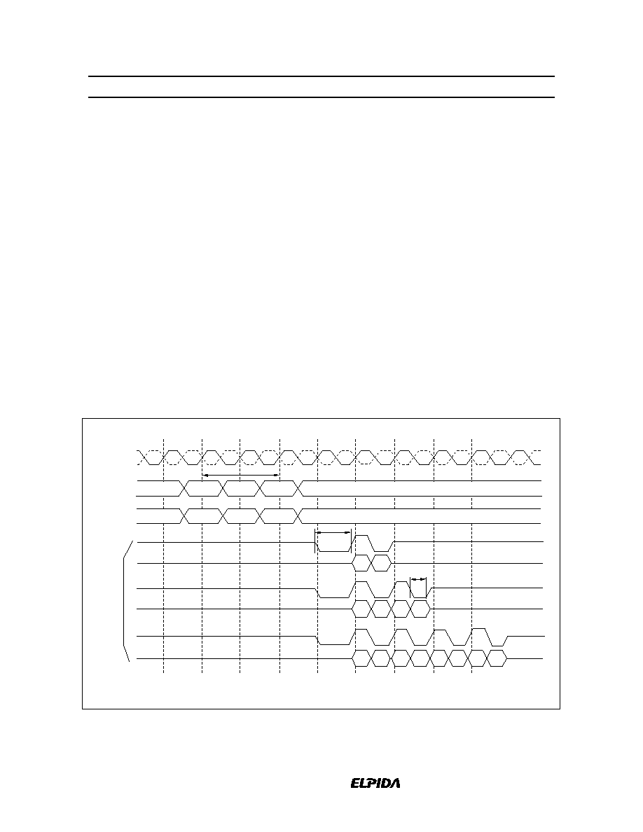
Read/Write Operations
Bank active: A read or a write operation begins with the bank active command [ACTV]. The bank active
command determines a bank address (BA0, BA1) and a row address (AX0 to AX12). For the bank and the
row, a read or a write command can be issued t
RCD
after the ACTV is issued.
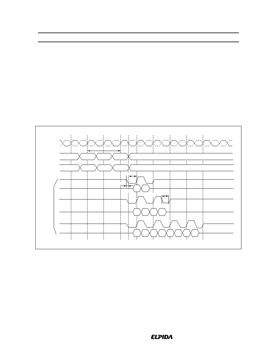
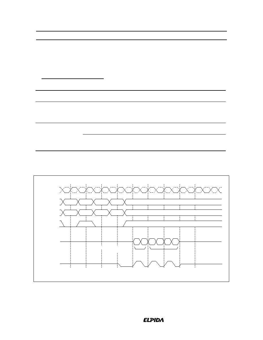
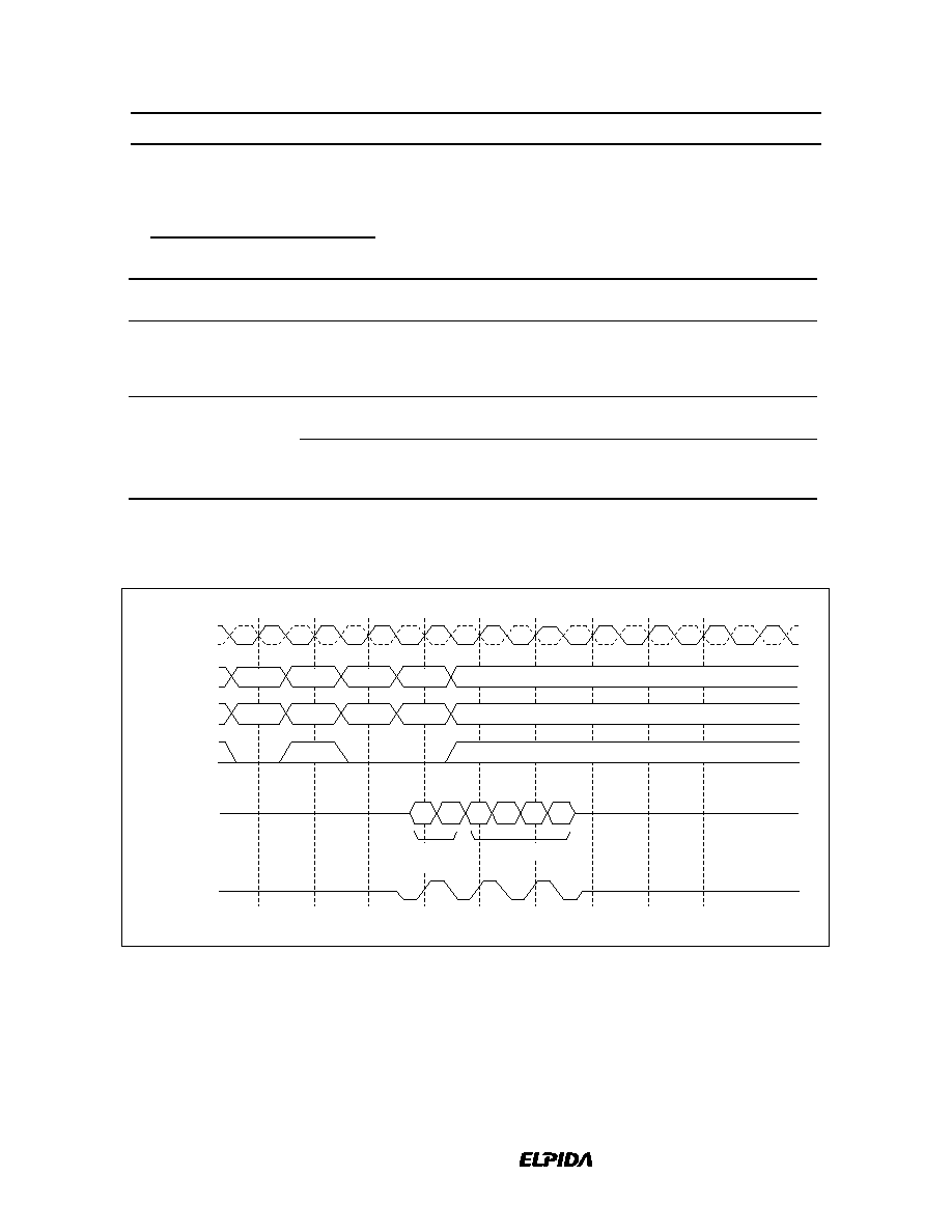
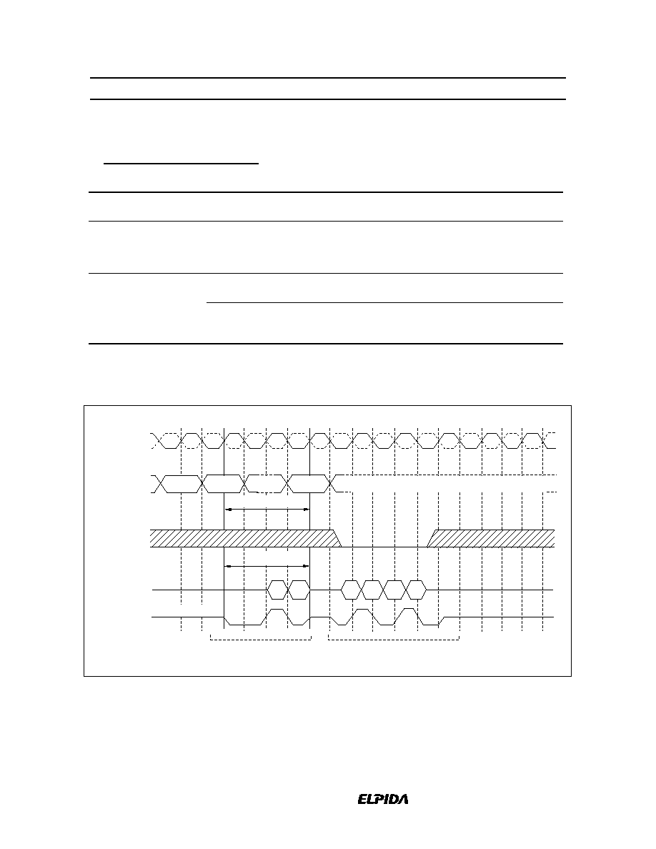
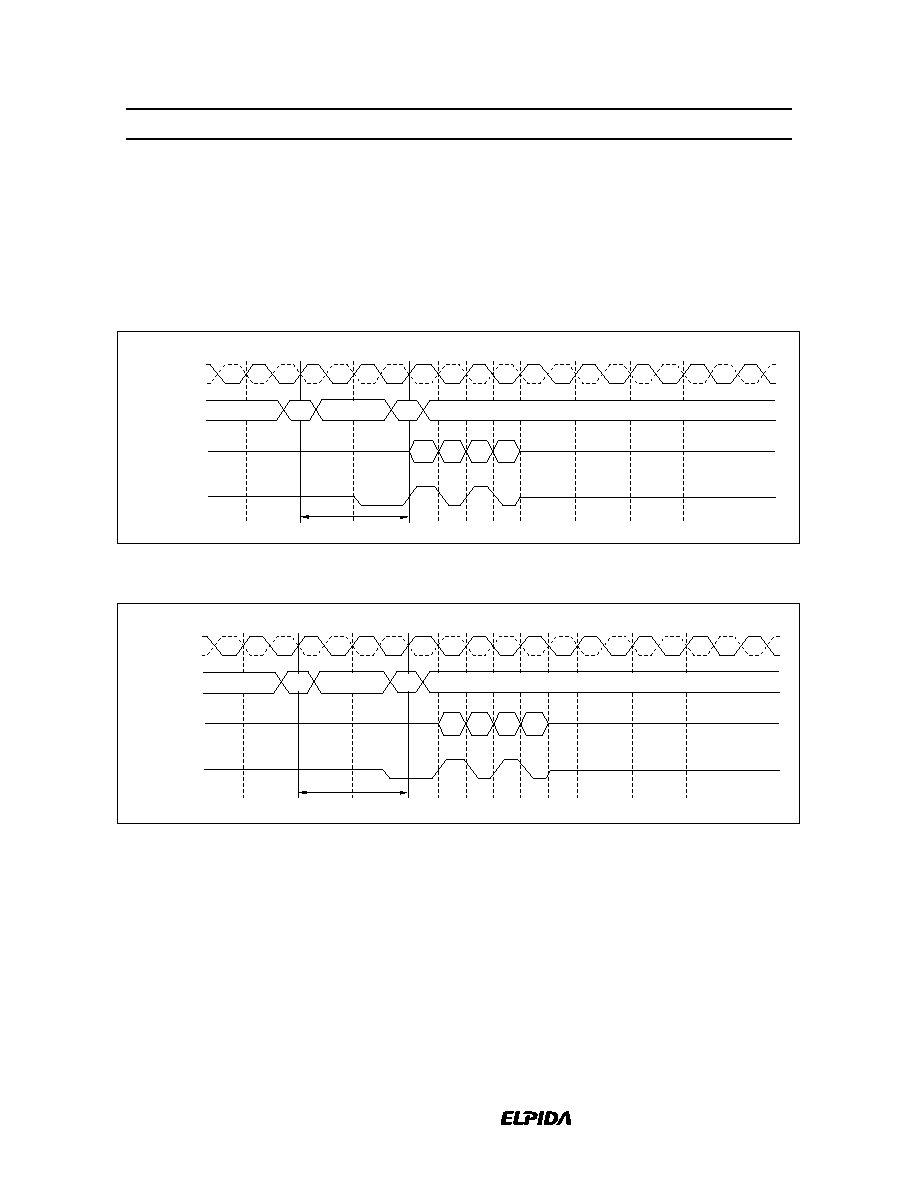
Read operation: The burst length (BL), the
CAS latency (CL) and the burst type (BT) of the mode register
are referred when a read command is issued. The burst length (BL) determines the length of a sequential
output data by the read command which can be set to 2, 4, or 8. The starting address of the burst read is
defined by the column address (AY0 to AY8; the HM5425161B, AY0 to AY9; the HM5425801B, AY0 to
AY9, AY11; the HM5425401B), the bank select address (BA0, BA1) which are loaded via the A0 to A12 and
BA0, BA1 pins in the cycle when the read command is issued. The data output timing are characterized by
CL (2 or 2.5) and t
AC
. The read burst start CL
∑
t
CK
+ t
AC
(ns) after the clock rising edge where the read
command are latched. The DDR SDRAM output the data strobe through DQS or DQSU/DQSL
simultaneously with data. t
RPRE
prior to the first rising edge of the data strobe, the DQS or the DQSU/DQSL
are driven Low from V
TT
level. This low period of DQS is referred as read preamble. The burst data are
output coincidentally at both the rising and falling edge of the data strobe. The DQ pins become High-Z in
the next cycle after the burst read operation completed. t
RPST
from the last falling edge of the data strobe, the
DQS pins become High-Z. This low period of DQS is referred as read postamble.
Read Operation
(Burst Length)
D0
D1
D0
D1
D2
D3
D0
D1
D2
D3
D4
D5
D6
D7
CLK
CLK
Address
DQS*
Dout
BL = 2
BL = 4
BL = 8
Command
CAS
latency = 2
BL: Burst length
t1
t0
t2
t3
t4
t5
t6
t7
t8
t
RCD
t
RPRE
DQS*:DQS,DUSU/DQSL
t
RPST
ACTV
NOP
NOP
NOP
READ
;
;;
;
Row
Column
HM5425161B, HM5425801B, HM5425401B Series
Data Sheet E0086H20
25
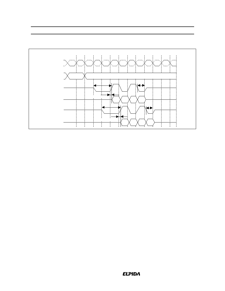
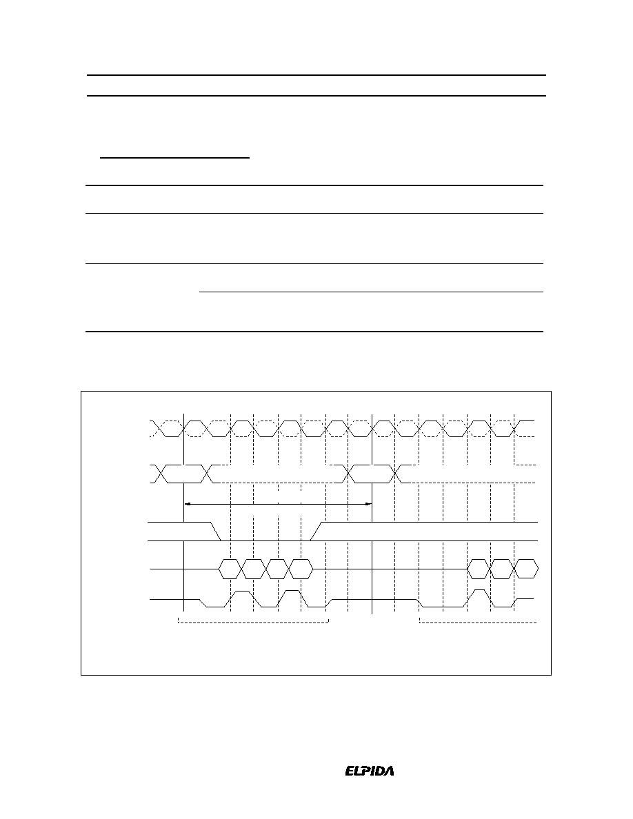
Read Operation
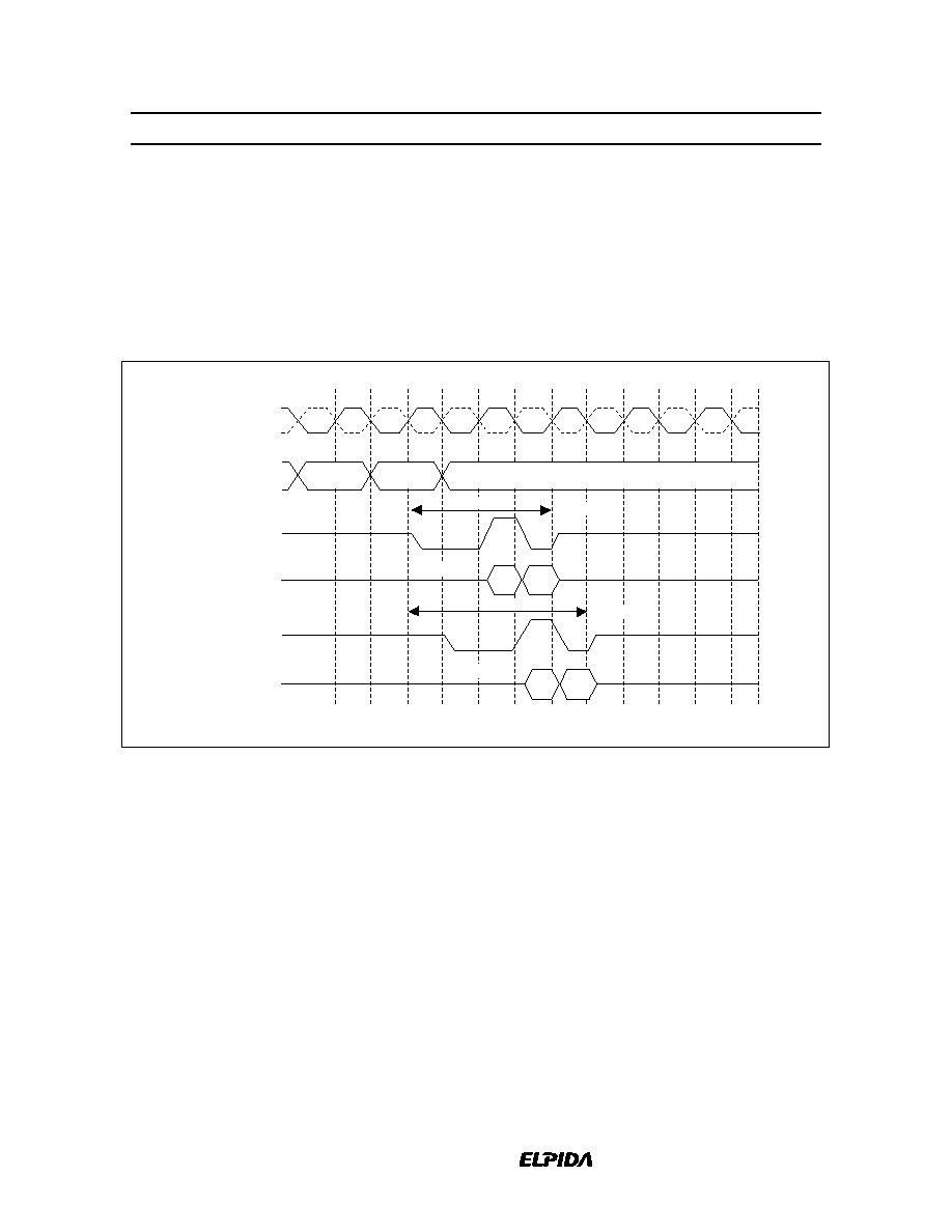
(CAS Latency)
CLK
CLK
DQS
V
TT
V
TT
V
TT
V
TT
DQ
DQS
DQ
CL = 2
CL = 2.5
Command
t0
t0.5
t1
t1.5
t2
t2.5
t3
t3.5
t4
t4.5
t5
t5.5
D0
D1
D2
D3
D0
D1
D2
D3
t
RPST
t
RPRE
t
RPRE
t
RPST
t
AC
,t
DQSCK
t
AC
,t
DQSCK
Read
NOP
HM5425161B, HM5425801B, HM5425401B Series
Data Sheet E0086H20
26
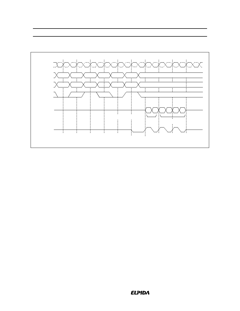
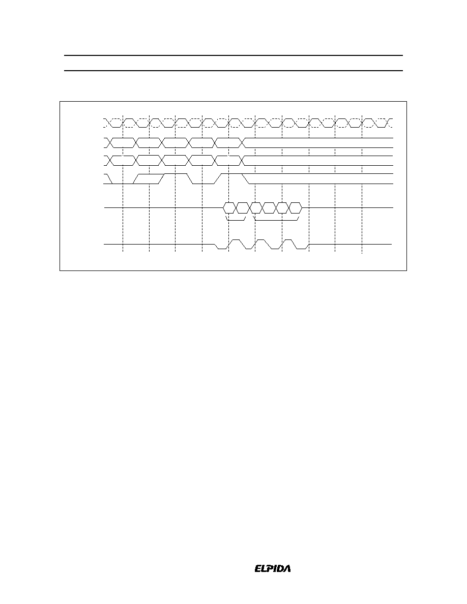
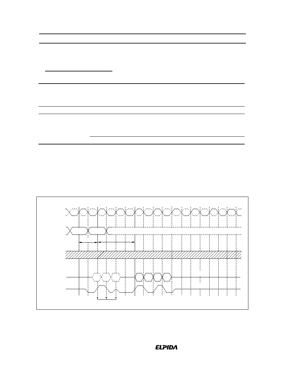
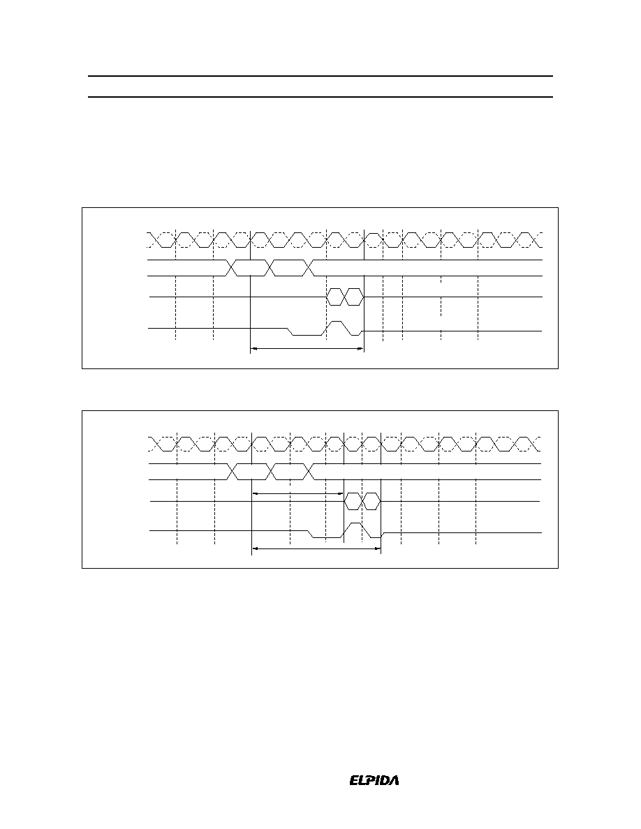
Write operation: The burst length (BL) and the burst type (BT) of the mode register are referred when a
write command is issued. The burst length (BL) determines the length of a sequential data input by the write
command which can be set to 2, 4, or 8. The latency from write command to data input is fixed to 1. The
starting address of the burst read is defined by the column address (AY0 to AY8; the HM5425161B, AY0 to
AY9; the HM5425801B, AY0 to AY9, AY11; the HM5425401B), the bank select address (BA0/BA1) which
are loaded via the A0 to A12, BA0 to BA1 pins in the cycle when the write command is issued. DQS,
DQSU/DQSL should be input as the strobe for the input-data and DM, DMU/DML as well during burst
operation. t
WPREH
prior to the first rising edge of the DQS, the DQSU/DQSL should be set to Low and t
WPST
after the last falling edge of the data strobe can be set to High-Z. The leading low period of DQS is referred
as write preamble. The last low period of DQS is referred as wrtie postamble.
Write Operation
in1
in0
in1
in2
in3
in0
in1
in2
in3
in4
in5
in6
in7
CLK
CLK
Address
DQS*
Din
BL = 2
BL = 4
BL = 8
Command
BL: Burst length
t1
t0
t2
t3
t3.5
t4
t5
t6
t7
t8
t
RCD
t
WPST
DQS*:DQS,DQSU/DQSL
in0
ACTV
NOP
NOP
NOP
WRITE
t
WPREH
t
WPRES
;;
;;;
;
;
Row
Column
HM5425161B, HM5425801B, HM5425401B Series
Data Sheet E0086H20
27
Burst Stop
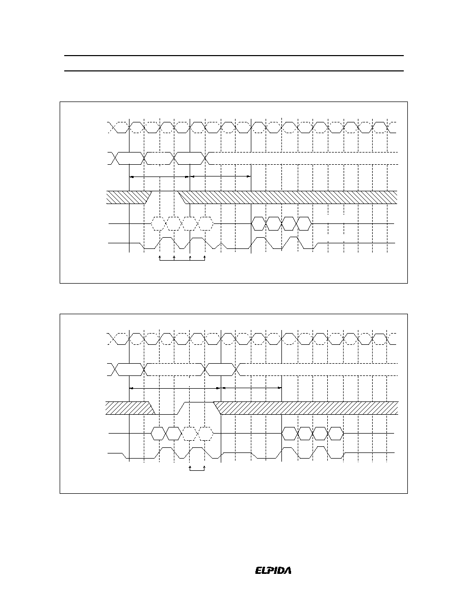
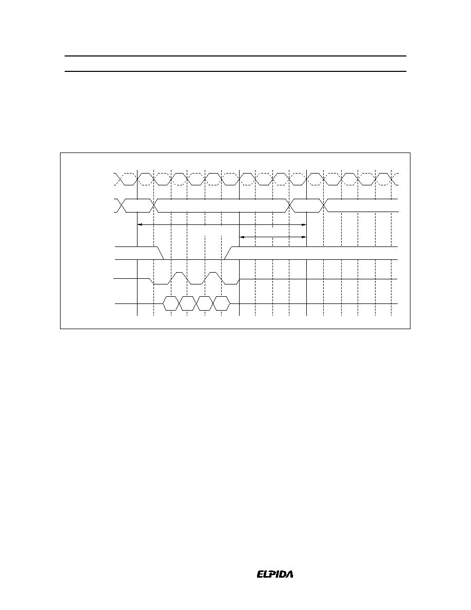
Burst stop command during burst read: The burst stop (BST) command is used to stop data output during
a burst read. The BST command stops the burst read and sets the output buffer to High-Z. t
BSTZ
(= CL) cycles
after a BST command issued, the DQ pins become High-Z. The BST command is not supported for the burst
write operation. Note that bank address is not referred when this command is executed.
Burst Stop during a Read Operation
CLK
CLK
DQS
DQ
DQS
DQ
CL = 2
CL = 2.5
Command
t0
t0.5
t1
t1.5
t2
t2.5
t3
t3.5
t4
t4.5
t5
t5.5
D0
D1
D0
D1
CL:
CAS
latency
Read
BST
NOP
2 cycles
t
BSTZ
t
BSTZ
2.5 cycles
HM5425161B, HM5425801B, HM5425401B Series
Data Sheet E0086H20
28
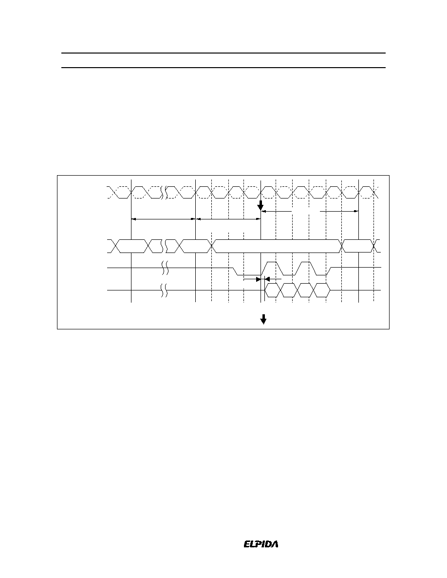
Auto Precharge
Read with auto-precharge: The precharge is automatically performed after completing a read operation.
The precharge starts t
RPD
(BL/2) cycle after READA command input. t
RAP
specification for READA allows a
read command with auto precharge to be issued to a bank that has been activated (opened) but has not yet
satisfied the t
RAS
(min) specification. A column command to the other active bank can be issued at the next
cycle after the last data output. Read with auto-precharge command does not limit row commands execution
for other bank. Refer to the `Read with Auto-Precharge Enabled, Write with Auto-Precharge Enabled'
section.
D0
D1
D2
D3
CLK
CLK
DQ
Command
t
RP
(min)
t
RAP
(min) = t
RCD
(min)
ACTV
Note: Internal auto-precharge starts at the timing indicated by " ".
NOP
2 cycles (= BL/2)
READA
ACTV
DQS,
DQSU/DQSL
t
AC
,t
DQSCK
t
RPD
HM5425161B, HM5425801B, HM5425401B Series
Data Sheet E0086H20
29
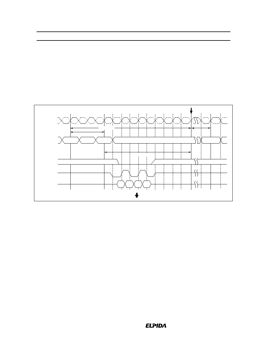
Write with auto-precharge: The precharge is automatically performed after completing a burst write
operation. The precharge operation is started t
WPD
(= BL/ 2 + 3) cycles after WRITA command issued. t
RCD
for WRITA should be determined so that t
RC
(ACTV to ACTV) spec. is obeyed when WRITA is issued
successively after a bank active command, that is t
RCD
(WRITA)
t
RC
(min.)-t
RP
(min.)-t
W P D
. A column
command to the other banks can be issued the next cycle after the internal precharge command issued. Write
with auto-precharge command does not limit row commands execution for other bank. Refer to the `Read
with Auto-Precharge Enabled, Write with Auto-Precharge Enabled' section
Burst Write (Burst Length = 4)
;;
D1
D2
D3
D4
CLK
CLK
DQ
Command
DM,
DMU/DML
t
RAS
(min)
t
RCD
(min)
;;
;
t
RP
DQS,
DQSU/DQSL
ACTV
WRITA
ACTV
BL/2 + 3 cycles
t
WPD
Note: Internal auto-precharge starts at the timing indicated by " ".
Burst length = 4
NOP
NOP
HM5425161B, HM5425801B, HM5425401B Series
Data Sheet E0086H20
30
Command Intervals
A Read command to the consecutive Read command Interval
Destination row of the
consecutive read command
Bank
address
Row
address
State
Operation
1. Same
Same
ACTIVE
The consecutive read can be performed after an interval of no less
than 1 cycle to interrupt the preceding read operation.
2. Same
Different
--
Precharge the bank to interrupt the preceding read operation. t
RP
after
the precharge command, issue the ACTV command. t
RCD
after the
ACTV command, the consecutive read command can be issued. See
`A read command to the consecutive precharge interval' section.
3. Different
Any
ACTIVE
The consecutive read can be performed after an interval of no less
than 1 cycle to interrupt the preceding read operation.
IDLE
Precharge the bank without interrupting the preceding read operation.
t
RP
after the precharge command, issue the ACTV command. t
RCD
after
the ACTV command, the consecutive read command can be issued.
READ to READ Command Interval (same ROW address in the same bank)
;;;
;
;
A0
A1
B0
B1
B2
B3
CLK
CLK
Address
BA
Dout
DQS,
DQSU/DQSL
Command
t1
t0
t2
t3
t4
t5
t6
t7
t8
Bank0
Active
Column = A
Dout
Column = B
Dout
;;;
;
;
;
CAS
latency = 2
Burst length = 4
Bank0
NOP
ACTV
NOP
READ
Row
Column A
READ
Column B
Column = A
Read
Column = B
Read
HM5425161B, HM5425801B, HM5425401B Series
Data Sheet E0086H20
31
READ to READ Command Interval (different bank)
;;
;
;;
;
A0
A1
B0
B1
B2
B3
CLK
CLK
Address
BA
Dout
DQS,
DQSU/DQSL
Command
t1
t0
t2
t3
t4
t5
t6
t7
t8
t9
Bank0
Active
Bank3
Active
Bank0
Read
Bank3
Read
Bank0
Dout
;;
;
;
;;
CAS
latency = 2
Burst length = 4
NOP
ACTV
NOP
NOP
Row0
ACTV
READ
Row1
Column A
READ
Column B
Column = A
Read
Column = B
Read
Bank3
Dout
HM5425161B, HM5425801B, HM5425401B Series
Data Sheet E0086H20
32
A Write command to the consecutive Write command Interval:
Destination row of the
consecutive write command
Bank
address
Row
address
State
Operation
1. Same
Same
ACTIVE
The consecutive write can be performed after an interval of no less
than 1 cycle to interrupt the preceding write operation.
2. Same
Different
--
Precharge the bank to interrupt the preceding write operation. t
RP
after
the precharge command, issue the ACTV command. t
RCD
after the
ACTV command, the consecutive write command can be issued. See
`A write command to the consecutive precharge interval' section.
3. Different
Any
ACTIVE
The consecutive write can be performed after an interval of no less
than 1 cycle to interrupt the preceding write operation.
IDLE
Precharge the bank without interrupting the preceding write operation.
t
RP
after the precharge command, issue the ACTV command. t
RCD
after
the ACTV command, the consecutive write command can be issued.
WRITE to WRITE Command Interval (same ROW address in the same bank)
;;;
;
;
;
A0
A1
B0
B1
B2
B3
CLK
CLK
Address
BA
Din
Command
t1
t0
t2
t3
t4
t5
t6
t7
t8
Bank0
Active
;;
;
;
;
Burst length = 4
Bank0
NOP
DQS,
DQSU/DQSL
ACTV
NOP
WRIT
Row
Column A
WRIT
Column B
Column = A
Write
Column = B
Write
HM5425161B, HM5425801B, HM5425401B Series
Data Sheet E0086H20
33
WRITE to WRITE Command Interval (different bank)
;
;;
;;
;
A0
A1
B0
B1
B2
B3
CLK
CLK
Address
BA
Din
Command
t1
t0
t2
t3
t4
t5
t6
t7
t8
t9
Bank0
Active
Bank3
Active
Bank0
Write
Bank3
Write
;;
;
;;
Burst length = 4
Bank0, 3
NOP
DQS,
DQSU/DQSL
ACTV
NOP
ACTV
WRIT
Row0
Row1
Column A
WRIT
Column B
HM5425161B, HM5425801B, HM5425401B Series
Data Sheet E0086H20
34
A Read command to the consecutive Write command interval with the BST command
Destination row of the
consecutive write command
Bank
address
Row
address
State
Operation
1. Same
Same
ACTIVE
Issue the BST command. t
BSTW
(
t
BSTZ
) after the BST command, the
consecutive write command can be issued.
2. Same
Different
--
Precharge the bank to interrupt the preceding read operation. t
RP
after
the precharge command, issue the ACTV command. t
RCD
after the
ACTV command, the consecutive write command can be issued. See
`A read command to the consecutive precharge interval' section.
3. Different
Any
ACTIVE
Issue the BST command. t
BSTW
(
t
BSTZ
) after the BST command, the
consecutive write command can be issued.
IDLE
Precharge the bank independently of the preceding read operation.
t
RP
after the precharge command, issue the ACTV command. t
RCD
after
the ACTV command, the consecutive write command can be issued.
READ to WRITE Command Interval
Q0
Q1
D0
D1
D2
D3
CLK
CLK
DM,
DMU/DML
DQ
Command
t1
t0
t2
t3
t4
t5
t6
t7
t8
Burst Length = 4
CAS
Latency= 2
DQS,
DQSU/DQSL
OUTPUT
INPUT
t
BSTW (
t
BSTZ)
High-Z
READ
WRIT
BST
NOP
NOP
t
BSTZ (= CL)
HM5425161B, HM5425801B, HM5425401B Series
Data Sheet E0086H20
35
A Write command to the consecutive Read command interval: To complete the burst operation
Destination row of the
consecutive read command
Bank
address
Row
address
State
Operation
1. Same
Same
ACTIVE
To complete the burst operation, the consecutive read command
should be performed t
WRD
(= BL/ 2 + 2) after the write command.
2. Same
Different
--
Precharge the bank t
WPD
after the preceding write command. t
RP
after
the precharge command, issue the ACTV command. t
RCD
after the
ACTV command, the consecutive read command can be issued. See
`A read command to the consecutive precharge interval' section.
3. Different
Any
ACTIVE
To complete a burst operation, the consecutive read command should
be performed t
WRD
(= BL/ 2 + 2) after the write command.
IDLE
Precharge the bank independently of the preceding write operation.
t
RP
after the precharge command, issue the ACTV command. t
RCD
after
the ACTV command, the consecutive read command can be issued.
WRITE to READ Command Interval
D0
D1
D2
D3
Q2
Q0
Q1
CLK
CLK
DM,
DMU/DML
DQ
Command
t1
t0
t2
t3
t4
t5
t6
;
;
;;
BL = 4
CL = 2
t
WRD
(min)
DQS,
DQSU/DQSL
INPUT
OUTPUT
BL/2 + 2 cycle
WRIT
NOP
NOP
READ
HM5425161B, HM5425801B, HM5425401B Series
Data Sheet E0086H20
36
A Write command to the consecutive Read command interval: To interrupt the write operation
Destination row of the
consecutive read command
Bank
address
Row
address
State
Operation
1. Same
Same
ACTIVE
DM, DMU/DML must be input 1 cycle prior to the read command input
to prevent from being written invalid data. In case, the read command
is input in the next cycle of the write command, DM, DMU/DML is not
necessary.
2. Same
Different
--
--*
1
3. Different
Any
ACTIVE
DM, DMU/DML must be input 1 cycle prior to the read command input
to prevent from being written invalid data. In case, the read command
is input in the next cycle of the write command, DM, DMU/DML is not
necessary.
IDLE
--*
1
Note:
1. Precharge must be preceded to read command. Therefore read command can not interrupt the
write operation in this case.
WRITE to READ Command Interval (Samebank, same ROW address)
[WRITE to READ delay = 1 clock cycle]
D0
D1
D2
Q0
Q1
Q2
Q3
CLK
CLK
DM,
DMU/DML
DQ
Command
t1
t0
t2
t3
t4
t5
t6
t7
t8
BL = 4
CL= 2
DQS,
DQSU/DQSL
CL=2
Data masked
1 cycle
READ
NOP
WRIT
High-Z
High-Z
HM5425161B, HM5425801B, HM5425401B Series
Data Sheet E0086H20
37
[WRITE to READ delay = 2 clock cycle]
D0
D1
D2
D3
Q0
Q1
Q2
Q3
CLK
CLK
DM,
DMU/DML
DQ
Command
t1
t0
t2
t3
t4
t5
t6
t7
t8
BL = 4
CL= 2
DQS,
DQSU/DQSL
CL=2
Data masked
2 cycle
READ
NOP
NOP
WRIT
High-Z
High-Z
[WRITE to READ delay = 3 clock cycle]
D0
D1
D2
D3
Q0
Q1
Q2
Q3
CLK
CLK
DM,
DMU/DML
DQ
Command
t1
t0
t2
t3
t4
t5
t6
t7
t8
BL = 4
CL= 2
DQS,
DQSU/DQSL
CL=2
Data masked
3 cycle
READ
WRIT
NOP
NOP
HM5425161B, HM5425801B, HM5425401B Series
Data Sheet E0086H20
38
A Read command to the consecutive Precharge command interval (same bank):
To output all data: To complete a burst read opeartion and get a burst length of data, the consecutive
precharge command must be issued t
RPD
(= BL/ 2 cycles) after the read command is issued.
READ to PRECHARGE Command Interval (same bank): To output all data
CAS Latency = 2, Burst Length = 4
A0
A1
A2
A3
CLK
CLK
Dout
DQS,
DQSU/DQSL
Command
t1
t0
t2
t3
t4
t5
t6
t7
t8
t
RPD
= BL/2
READ
NOP
NOP
NOP
PRE/
PALL
CAS Latency = 2.5, Burst Length = 4
A0
A1
A2
A3
CLK
CLK
Dout
DQS,
DQSU/DQSL
Command
t1
t0
t2
t3
t4
t5
t6
t7
t8
t
RPD
= BL/2
READ
NOP
NOP NOP
PRE/
PALL
HM5425161B, HM5425801B, HM5425401B Series
Data Sheet E0086H20
39
READ to PRECHARGE Command Interval (same bank): To stop output data
A burst data output can be interrupted with a precharge command. All DQ pins and DQS pins become High-
Z t
HZP
(= CL) after the precharge command.
CAS Latency = 2, Burst Length = 2, 4, 8
A0
A1
CLK
CLK
Dout
DQS,
DQSU/DQSL
Command
t1
t0
t2
t3
t4
t5
t6
t7
t8
PRE/PALL
t
HZP
= CL + 1
READ
NOP
NOP
High-Z
High-Z
CAS Latency = 2.5, Burst Length = 2, 4, 8
A0
A1
CLK
CLK
Dout
DQS,
DQSU/DQSL
Command
t1
t0
t2
t3
t4
t5
t6
t7
t8
High-Z
High-Z
t
HZP
= CL + 1
CL = 2.5
READ
NOP
NOP
PRE/PALL
HM5425161B, HM5425801B, HM5425401B Series
Data Sheet E0086H20
40
A Write command to the consecutive Precharge command interval (same bank): The minimum interval
t
WPD
((BL/ 2 + 3) cycles) is necessary between the write command and the precharge command.
WRITE to PRECHARGE Command Interval (same bank)
Burst Length = 4
A0
A1
A2
A3
CLK
CLK
Din
DM,
DMU/DML
DQS,
DQSU/DQSL
Command
t1
t0
t2
t3
t4
t5
t6
t7
Last data input
t
WPD
;
;
;
;;
WRIT
NOP
NOP
t
WR
BL/2 +3 cycles
PRE/PALL

HM5425161B, HM5425801B, HM5425401B Series
Data Sheet E0086H20
41
Bank active command interval:
Destination row of the
consecutive ACTV command
Bank
address
Row
address
State
Operation
1. Same
Any
ACTIVE
Two successive ACTV commands can be issued at t
RC
interval. In
between two successive ACTV operations, precharge command
should be executed.
2. Different
Any
ACTIVE
Prechage the bank. t
RP
after the precharge command, the consecutive
ACTV command can be issued.
IDLE
t
RRD
after an ACTV command, the next ACTV command can be issued.
Bank Active to Bank Active
CLK
CLK
Command
BA
t
RC
Address
;
;
;
;
;;
;
ACTV
t
RRD
Bank0
Active
Bank3
Active
Bank0
Precharge
Bank0
Active
;;
;
PRE
;;
ACTV
ROW: 0
NOP
NOP
NOP
ACTV
;;
ACTV
ROW: 1
ROW: 0
Mode register set to Bank-active command interval: The interval between setting the mode register and
executing a bank-active command must be no less than t
MRD
.
CLK
CLK
Command
Address
NOP
NOP
MRS
ACTV
t
MRD
Mode Register Set
Bank3
Active
;
;
CODE
BS and ROW
HM5425161B, HM5425801B, HM5425401B Series
Data Sheet E0086H20
42
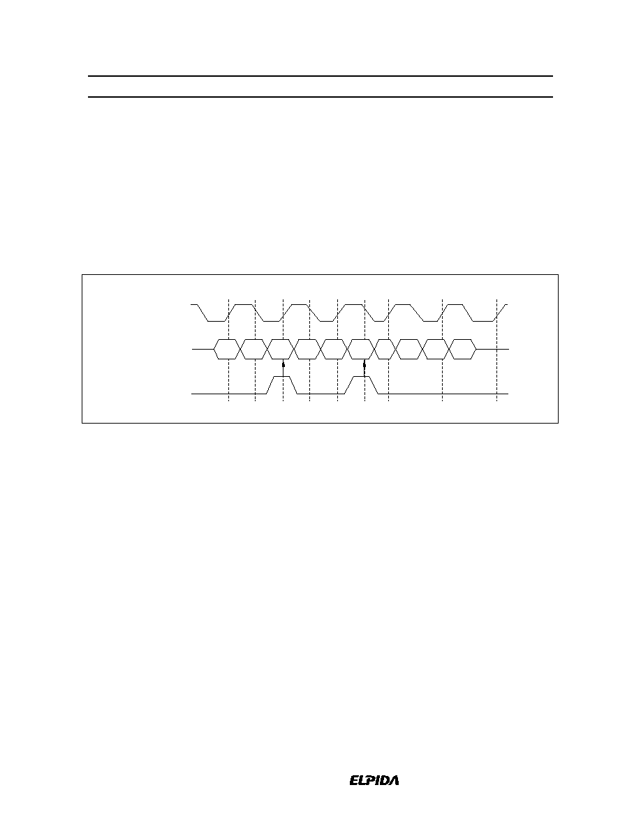
DMU/DML Control (HM5425161B)
DMU can mask upper byte of input data. DML can mask lower byte of input data. By setting DMU/DML to
Low, data can be written. When DMU/DML is set to High, the corresponding data is not written, and the
previous data is held. The latency between DMU/DML input and enabling/disabling mask function is 0.
DM Control (HM5425801B/HM5425401B)
DM can mask input data. By setting DM to Low, data can be written. When DM is set to High, the
corresponding data is not written, and the previous data is held. The latency between DM input and
enabling/disabling mask function is 0.
Mask
Mask
DQS,
DQSU/DQSL
DQ
DM,
DMU/DML
t1
t2
t3
t4
t5
t6
Write mask latency = 0
HM5425161B, HM5425801B, HM5425401B Series
Data Sheet E0086H20
43
Absolute Maximum Ratings
Parameter
Symbol
Value
Unit
Note
Supply voltage relative to V
SS
V
CC
, V
CCQ
≠1.0 to +3.6
V
Voltage on inputs pin relative to V
ss
Vti
≠1.0 to +3.6
V
Voltage on I/O pins relative to V
SS
VTio
≠0.5 to +3.6
V
Short circuit output current
Iout
50
mA
Power dissipation
P
T
1.0
W
Operating temperature
Topr
0 to +70
∞C
Storage temperature
Tstg
≠55 to +125
∞C
DC Operating Conditions (Ta = 0 to +70∞C)
Parameter
Symbol
Min
Typ
Max
Unit
Notes
Supply voltage
V
CC
, V
CCQ
2.3
2.5
2.7
V
1, 2
V
SS
, V
SSQ
0
0
0
V
Input reference voltage
V
REF
(DC)
0.5
◊
V
CCQ
≠0.05
0.5
◊
V
CCQ
0.5
◊
V
CCQ
+0.05
V
1
Termination voltage
V
TT
V
REF
≠
0.04
V
REF
V
REF
+0.04
V
1
DC Input high voltage
V
IH
(DC)
V
REF
+0.15
--
V
CCQ
+0.3
V
1, 3, 8
DC Input low voltage
V
IL
(DC)
≠0.3
--
V
REF
≠0.15
V
1, 4, 8
DC Input signal voltage
(CLK, /CLK)
V
IN
(DC)
≠0.3
--
V
CCQ
+ 0.3
V
5
DC differential input voltage
(CLK, /CLK)
V
ID
(DC)
0.36
--
V
CCQ
+ 0.6
V
6, 7
Notes: 1. All parameters are referred to V
SS
, when measured.
2. V
CCQ
must be lower than or equal to V
CC
.
3. V
IH
is allowed to exceed V
CC
up to 3.6 V for the period shorter than or equal to 5 ns.
4. V
IL
is allowed to outreach below V
SS
down to ≠1.0 V for the period shorter than or equal to 5 ns.
5. V
IN
(dc) specifies the allowable dc execution of each differential input.
6. V
ID
(dc) specifies the input differential voltage required for switching.
7. V
IH
(CLK) min assumed over V
REF
+ 0.15 V, V
IL
(CLK) max assumed under V
REF
≠ 0.15 V.
8. V
IH
(DC) and V
IL
(DC) are levels to maintain the current logic state.
HM5425161B, HM5425801B, HM5425401B Series
Data Sheet E0086H20
44
DC Characteristics 1 (Ta = 0 to +70∞C, V
CC
, V
CCQ
= 2.5 V ± 0.2 V, V
SS
, V
SSQ
= 0 V)
Parameter
Symbol
Min
Max
Unit
Test conditions
Notes
Input leakage current
I
LI
≠2
2
µA
V
CC
Vin
V
SS
Output leakage current
I
LO
≠5
5
µA
V
CCQ
Vout
V
SSQ
Output high voltage
V
OH
1.95
--
V
I
OH
(max) = ≠15.2 mA
Output low voltage
V
OL
--
0.35
V
I
OL
(min) = 15.2 mA
HM5425161B, HM5425801B, HM5425401B Series
Data Sheet E0086H20
45
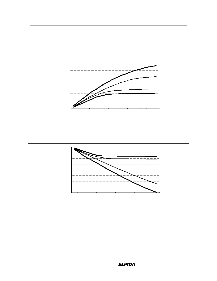
Data Driver Output Characteristic Curves
1. The full variation in driver pulldown current from minimum to maximum temperature and voltage will lie
within the outer bounding lines of the V-I curve of the figure "Pull-down Characteristics".
0
25
50
75
100
125
150
0
0.2 0.4 0.6 0.8
1
1.2 1.4 1.6 1.8
2
2.2 2.4 2.6 2.8
VOUT to VSSQ (V)
Pulldown Current (mA)
Minimum
Typical High
Typical Low
Maximum
Pull-down Characteristics
2. The full variation in driver pullup current from minimum to maximum temperature and voltage will lie
within the outer bounding lines of the V-I curve of the figure "Pull-up Characteristics".
-200
-175
-150
-125
-100
-75
-50
-25
0
0
0.2 0.4 0.6 0.8
1
1.2 1.4 1.6 1.8
2
2.2 2.4 2.6 2.8
VDDQ to VOUT (V)
Pullup Current (mA)
Minimum
Typical High
Typical Low
Maximum
Pull-up Characteristics
5. The full variation in the ratio of the maximum to minimum pullup and pulldown current will not exceed
1.7 for device drain to source voltages from 0.1 to 1.0.
6. The full variation in the ratio of the typical IBIS pullup to typical IBIS pulldown current should be unity
±
10%, for device drain to source voltages from 0.1 to 1.0. This specification is a design objective only.
7. These characteristics obey the SSTL_2 class II standard.
HM5425161B, HM5425801B, HM5425401B Series
Data Sheet E0086H20
46
Data Driver Output Characteristic V-I data points
Evaluation Conditions
∑
Typical: Ta = 25
∞
C, V
CCQ
= 2.5 V
∑
Minimum: Ta = 70
∞
C, V
CCQ
= 2.3 V
∑
Maximum: Ta = 0
∞
C, V
CCQ
= 2.7 V
Pull-down current (mA)
Pull-up current (mA)
Voltage (V)
Typical
Low
Typical
High
Minimum
Maximum
Typical
Low
Typical
High
Minimum
Maximum
0.1
6.0
6.8
4.6
9.6
≠6.1
≠7.6
≠4.6
≠10.0
0.2
12.2
13.5
9.2
18.2
≠12.2
≠14.5
≠9.2
≠20.0
0.3
18.1
20.1
13.8
26.0
≠18.1
≠21.2
≠13.8
≠29.8
0.4
24.1
26.6
18.4
33.9
≠24.0
≠27.7
≠18.4
≠38.8
0.5
29.8
33.0
23.0
41.8
≠29.8
≠34.1
≠23.0
≠46.8
0.6
34.6
39.1
27.7
49.4
≠34.3
≠40.5
≠27.7
≠54.4
0.7
39.4
44.2
32.2
56.8
≠38.1
≠46.9
≠32.2
≠61.8
0.8
43.7
49.8
36.8
63.2
≠41.1
≠53.1
≠36.0
≠69.5
0.9
47.5
55.2
39.6
69.9
≠43.8
≠59.4
≠38.2
≠77.3
1
51.3
60.3
42.6
76.3
≠46.0
≠65.5
≠38.7
≠85.2
1.1
54.1
65.2
44.8
82.5
≠47.8
≠71.6
≠39.0
≠93.0
1.2
56.2
69.9
46.2
88.3
≠49.2
≠77.6
≠39.2
≠100.6
1.3
57.9
74.2
47.1
93.8
≠50.0
≠83.6
≠39.4
≠108.1
1.4
59.3
78.4
47.4
99.1
≠50.5
≠89.7
≠39.6
≠115.5
1.5
60.1
82.3
47.7
103.8
≠50.7
≠95.5
≠39.9
≠123.0
1.6
60.5
85.9
48.0
108.4
≠51.0
≠101.3
≠40.1
≠130.4
1.7
61.0
89.1
48.4
112.1
≠51.1
≠107.1
≠40.2
≠136.7
1.8
61.5
92.2
48.9
115.9
≠51.3
≠112.4
≠40.3
≠144.2
1.9
62.0
95.3
49.1
119.6
≠51.5
≠118.7
≠40.4
≠150.5
2
62.5
97.2
49.4
123.3
≠51.6
≠124.0
≠40.5
≠156.9
2.1
62.9
99.1
49.6
126.5
≠51.8
≠129.3
≠40.6
≠163.2
2.2
63.3
100.9
49.8
129.5
≠52.0
≠134.6
≠40.7
≠169.6
2.3
63.8
101.9
49.9
132.4
≠52.2
≠139.9
≠40.8
≠176.0
2.4
64.1
102.8
50.0
135.0
≠52.3
≠145.2
≠40.9
≠181.3
2.5
64.6
103.8
50.2
137.3
≠52.5
≠150.5
≠41.0
≠187.6
2.6
64.8
104.6
50.4
139.2
≠52.7
≠155.3
≠41.1
≠192.9
2.7
65.0
105.4
50.5
140.8
≠52.8
≠160.1
≠41.2
≠198.2

HM5425161B, HM5425801B, HM5425401B Series
Data Sheet E0086H20
47
DC Characteristics 2*
1
(Ta = 0 to +70∞C, V
CC
, V
CCQ
= 2.5 V ± 0.2 V, V
SS
, V
SSQ
= 0 V)
Max
Parameter
Symbol
I/O
-75A
-75B
-10
Unit
Operating current (ACTV-
PRE)
I
CC0
100
95
80
mA
Operating current (ACTV-
READ-PRE)
I
CC1
155
145
130
mA
Idle power down standby
current
I
CC2P
18
15
12
mA
Idle standby current
I
CC2N
40
35
30
mA
Active power down
standby current
I
CC3P
25
20
15
mA
Active standby current
I
CC3N
50
45
40
mA
Operating current
(Burst read operation)
I
CC4R
◊
4,
◊
8
◊
16
225
255
215
245
205
235
mA
Operating current
(Burst write operation)
I
CC4W
◊
4,
◊
8
◊
16
205
240
195
230
185
220
mA
Auto Refresh current
I
CC5
205
200
180
mA
Self refresh current
I
CC6
3
3
3
mA
Random read current
I
CC7A
◊
4,
◊
8
◊
16
330
360
320
350
310
340
mA
Notes: 1. These I
CC
data are measured under condition that DQ pins are not connected.

HM5425161B, HM5425801B, HM5425401B Series
Data Sheet E0086H20
48
ICC Measurement Condition
Parameter
Symbol
Condition
Operating current
(ACTV-PRE)
I
CC0
One Bank ; CKE
V
IH
(min), t
RC
= t
RC
(min); t
CK
= t
CK
(min);
DQ, DM and DQS inputs changing twice per clock cycle; address
and control inputs changing once per clock cycle
Operating current
(ACTV-READ-PRE)
I
CC1
One Bank; CKE
V
IH
(min); Burst = 2; t
RC
= t
RC
(min); CL = 2.5; t
CK
= t
CK
(min); Iout = 0 mA; address and control inputs changing once
per clock cycle
Idle power down standby
current
I
CC2P
All banks idle; power down mode; CKE
V
IL
(max); t
CK
= t
CK
(min).
Vin = V
REF
for DQ, DQS and DM
Idle standby current
I
CC2N
All banks idle;
CS
V
IH
(min); CKE
V
IH
(min); t
CK
= t
CK
(min);
Address and other control inputs changing once per clock cycle.
Vin
V
IH
(min) or Vin
V
IL
(max) for DQ, DQS and DM.
Active power down standby
current
I
CC3P
One bank active; power down mode; CKE
V
IL
(max); t
CK
= t
CK
(min)
Active standby current
I
CC3N
One bank; Active Precharge;
CS
V
IH
(min); CKE
V
IH
(min); t
RC
=
t
RAS
(max); t
CK
= t
CK
(min); DQ,DM and DQS inputs changing twice
per clock cycle; address and other control inputs changing once
per clock cycle
Operating current
(Burst read operation)
I
CC4R
One bank active ; CKE
V
IH
(min); Burst = 2; Reads; Continuous
burst; address and control inputs changing once per clock cycle;
CL = 2.5; t
CK
= t
CK
(min); Iout = 0 mA;
Operating current
(Burst write operation)
I
CC4W
One bank active; CKE
V
IH
(min); Burst = 2; Writes; Continuous
burst; address and control inputs changing once per clock cycle;
CL = 2.5; t
CK
= t
CK
(min); DQ, DM and DQS inputs changing twice
per clock cycle
Auto refresh current
I
CC5
t
RC
= t
RFC
(min); Vin
V
IL
(max) or
V
IH
(min)
Self refresh current
I
CC6
CKE
0.2 V, Vin
0.2V or
V
CCQ
≠0.2V
Random read current
I
CC7A
4 banks active read with activate every 2 clocks, AP (Auto
Precharge) read every 2 clocks, BL = 4, t
RCD
=3, Iout = 0 mA,
100% DQ, DM and DQS inputs changing twice per clock cycle;
100% addresses changing once per clock cycle.
HM5425161B, HM5425801B, HM5425401B Series
Data Sheet E0086H20
49
Capacitance (Ta = 25∞C, V
CC
, V
CCQ
= 2.5 V ± 0.2 V)
Parameter
Symbol
Min
Max
Unit
Notes
Input capacitance (CLK,
CLK
)
C
I1
2
3
pF
1
Input capacitance (input only pins; including CKE
but not including CLK,
CLK
)
C
I2
2
3
pF
1
Input/output capacitance (DQ, DM, DQS)
C
IO
4
5
pF
1, 2
Delta input /output capacitance (DQ, DM, DQS)
C
IOD
0.5
pF
1
Delta input capacitance (CLK,
CLK
only)
C
ID
0.25
pF
1
Notes: 1. These parameters are measured on conditions: f = 100 MHz, Vout = V
CCQ
/2,
Vout = 0.2 V.
2. Dout circuits are disabled.

HM5425161B, HM5425801B, HM5425401B Series
Data Sheet E0086H20
50
AC Characteristics (Ta = 0 to +70∞C, V
CC
, V
CCQ
= 2.5 V ± 0.2 V, V
SS
, V
SSQ
= 0 V)
HM5425161B/HM542581B/HM5425401B
-75A
-75B
-10
Parameter
Symbol Min
Max
Min
Max
Min
Max
Unit
Notes
Clock cycle time
(
CAS
latency = 2)
t
CK
7.5
12
10
12
10
12
ns
10
(
CAS
latency = 2.5)
t
CK
7
12
7.5
12
8
12
ns
Input clock high level time
t
CH
0.45
0.55
0.45
0.55
0.45
0.55
t
CK
Input clock low level time
t
CL
0.45
0.55
0.45
0.55
0.45
0.55
t
CK
CLK half period
t
HP
min
(t
CH
, t
CL
)
--
min
(t
CH
, t
CL
)
--
min
(t
CH
, t
CL
)
--
t
CK
CLK to DQS skew
t
DQSCK
≠0.75
0.75
≠0.75
0.75
≠0.8
0.8
ns
2, 11
DATA to CLK skew
t
AC
≠0.75
0.75
≠0.75
0.75
≠0.8
0.8
ns
2, 11
Dout to DQS skew
t
DQSQ
--
0.5
--
0.5
--
0.6
ns
3
DQ/DQS output skew
hold time
t
QH
t
HP
≠ t
QHS
--
t
HP
≠ t
QHS
--
t
HP
≠ t
QHS
--
t
CK
Data hold skew factor
t
QHS
--
0.75
--
0.75
--
1.0
ns
Dout/DQS valid window
t
DV
0.35
--
0.35
--
0.35
--
t
CK
DQS valid window
t
DQSV
0.35
--
0.35
--
0.35
--
t
CK
DQS read preamble
t
RPRE
0.9
1.1
0.9
1.1
0.9
1.1
t
CK
DQS read postamble
t
RPST
0.4
0.6
0.4
0.6
0.4
0.6
t
CK
Dout-High impedance delay
from CLK/
CLK
t
HZ
≠0.75
0.75
≠0.75
0.75
≠0.8
0.8
ns
5, 11
Dout-Low impedance delay
from CLK/
CLK
t
LZ
≠0.75
0.75
≠0.75
0.75
≠0.8
0.8
ns
6, 11
DQ and DM input pulse
width
t
DIPW
1.75
--
1.75
--
2
--
ns
7
Data and data mask to data
strobe setup time
t
DS
0.5
--
0.5
--
0.6
--
ns
8
Data and data mask to data
strobe hold time
t
DH
0.5
--
0.5
--
0.6
--
ns
8
Clock to DQS write
preamble setup time
t
WPRES
0
--
0
--
0
--
ns
Clock to DQS write
preamble hold time
t
WPREH
0.25
--
0.25
--
0.25
--
t
CK
DQS last edge to High-Z
time (DQS write postamble)
t
WPST
0.4
0.6
0.4
0.6
0.4
0.6
t
CK
9

HM5425161B, HM5425801B, HM5425401B Series
Data Sheet E0086H20
51
HM5425161B/HM5425801B/HM5425401B
-75A
-75B
-10
Parameter
Symbol Min
Max
Min
Max
Min
Max
Unit
Notes
Clock to the DQS first rising
edge for write delay
t
DQSS
0.72
1.28
0.72
1.28
0.75
1.25
t
CK
DQS falling edge to CLK setup
time
t
DSS
0.2
--
0.2
--
0.2
--
t
CK
DQS falling edge hold time to
CLK
t
DSH
0.2
--
0.2
--
0.2
--
t
CK
DQS high pulse width
(DQS write)
t
DQSH
0.35
--
0.35
--
0.35
--
t
CK
DQS low pulse width
(DQS write)
t
DQSL
0.35
--
0.35
--
0.35
--
t
CK
Input command and address
setup time
t
IS
0.9
--
0.9
--
1.1
--
ns
8
Input command and address
hold time
t
IH
0.9
--
0.9
--
1.1
--
ns
8
RAS to READ (with auto
precharge)
t
RAP
20
--
20
--
20
--
ns
Active command period
t
RC
65
--
65
--
70
--
ns
Auto refresh to active/Auto
refresh command cycle
t
RFC
75
--
75
--
80
--
ns
Active to Precharge command
period
t
RAS
45
120000 45
120000 50
120000 ns
Active to column command
period
t
RCD
20
--
20
--
20
--
ns
Write recovery time
t
WR
15
--
15
--
15
--
ns
Auto precharge write recovery
and precharge time
t
DAL
35
--
35
--
40
--
ns
Precharge to active command
period
t
RP
20
--
20
--
20
--
ns
Active to active command
period
t
RRD
15
--
15
--
15
--
ns
Average periodic refresh
interval
t
REF
--
7.8
--
7.8
--
7.8
µs

HM5425161B, HM5425801B, HM5425401B Series
Data Sheet E0086H20
52
Notes: 1. On all AC measurements, we assume the test conditions shown in the next page. For timing
parameter definitions, see `Timing Waveforms' section.
2. This parameter defines the signal transition delay from the cross point of CLK and
CLK
. The signal
transition is defined to occur when the signal level crossing V
TT
.
3. The timing reference level is V
TT
.
4. Output valid window is defined to be the period between two successive transition of data out or
DQS (read) signals. The signal transition is defined to occur when the signal level crossing V
TT
.
5. t
HZ
is defined as Dout transition delay from Low-Z to High-Z at the end of read burst operation. The
timing reference is cross point of CLK and
CLK
. This parameter is not referred to a specific Dout
voltage level, but specify when the device output stops driving.
6. t
LZ
is defined as Dout transition delay from High-Z to Low-Z at the beginning of read operation. This
parameter is not referred to a specific Dout voltage level, but specify when the device output begins
driving.
7. Input valid windows is defined to be the period between two successive transition of data input or
DQS (write) signals. The signal transition is defined to occur when the signal level crossing V
REF
.
8. The timing reference level is V
REF
.
9. The transition from Low-Z to High-Z is defined to occur when the device output stops driving. A
specific reference voltage to judge this transition is not given.
10. t
CK
max is determined by the lock range of the DLL. Beyond this lock range, the DLL operation is
not assured.
11. t
CK
= min when these parameters are measured. Otherwise, absolute minimum value of these
values are 10% of t
CK
.
12. V
CC
is assumed to be 2.5 V ± 0.2 V. V
CC
power supply variation per cycle expected to be less than
0.4 V/400 cycle.
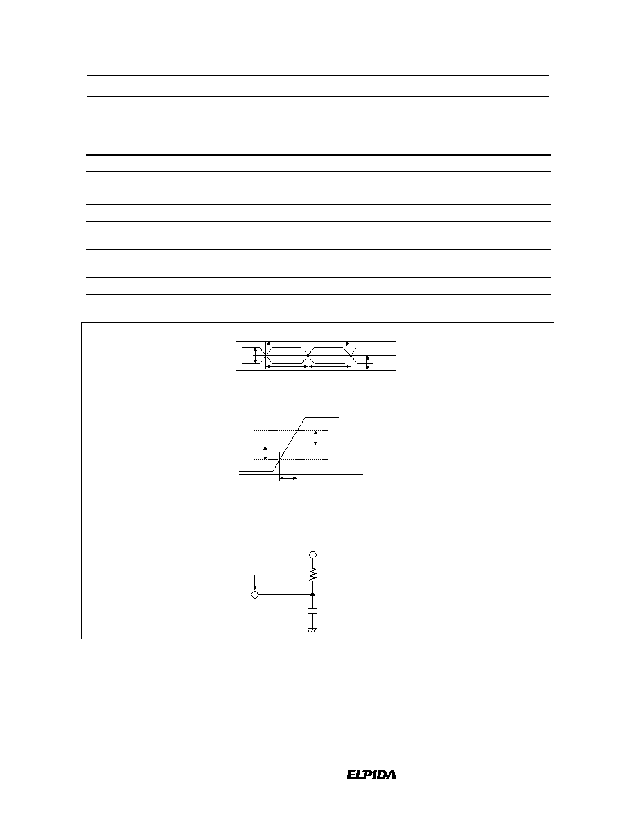
HM5425161B, HM5425801B, HM5425401B Series
Data Sheet E0086H20
53
Test Conditions
Parameter
Symbol
Min
Typ
Max
Unit
Input reference voltage
V
REF
(AC)
0.5
◊
V
CCQ
≠0.05
0.5
◊
V
CCQ
0.5
◊
V
CCQ
+0.05
V
Termination voltage
V
TT
(AC)
V
REF
(AC)
-
0.04
V
REF
(AC)
V
REF
(AC)
+
0.04 V
AC input high voltage
V
IH
(AC)
V
REF
(AC)
+
0.31
--
--
V
AC input low voltage
V
IL
(AC)
--
--
V
REF
(AC)
-
0.31 V
AC differential input voltage (CLK,
CLK
)
V
ID
(AC)
0.7
--
V
CCQ
+ 0.6
V
AC differential cross point voltage
(CLK,
CLK
)
V
X
(AC)
0.5
◊
V
CCQ
-
0.2
0.5
◊
V
CCQ
0.5
◊
V
CCQ
+
0.2 V
Input signal slew rate
SLEW
--
1
--
V/ns
V
TT
V
REF
(AC)
CLK
CLK
V
REF
V
SS
SLEW = (V
IH
(AC) ≠ V
IL
(AC))/
t
Measurement point
V
IH
V
IL
V
CC
V
CC
V
SS
DQ
R
T
= 50
C
L
= 30 pF
V
X
(AC)
t
t
CL
t
CK
t
CH
V
ID
(AC)

HM5425161B, HM5425801B, HM5425401B Series
Data Sheet E0086H20
54
Timing Parameter Measured in Clock Cycle
Number of clock cycle
Parameter
Symbol
Min
Max
Write to pre-charge command delay (same bank)
t
WPD
3 + BL/2
Read to pre-charge command delay (same bank)
t
RPD
BL/2
Write to read command delay (to input all data)
t
WRD
2 + BL/2
Burst stop command to write command delay
(
CAS
latency = 2)
t
BSTW
2
(
CAS
latency = 2.5)
t
BSTW
3
Burst stop command to DQ High-Z
(
CAS
latency = 2)
t
BSTZ
2
(
CAS
latency = 2.5)
t
BSTZ
2.5
Read command to write command delay (to output all data)
(
CAS
latency = 2)
t
RWD
2 + BL/2
(
CAS
latency = 2.5)
t
RWD
3 + BL/2
Pre-charge command to High-Z
(
CAS
latency = 2)
t
HZP
2
(
CAS
latency = 2.5)
t
HZP
2.5
Write command to data in latency
t
WCD
1
Auto precharge write recovery and precharge time
t
DAL
5
Write recovery
t
WR
2
DM to data in latency
t
DMD
0
Register set command to active or register set command
t
MRD
2
Self refresh exit to non-read command
t
SNR
10
Self refresh exit to read command
t
SRD
200
Power down entry
t
PDEN
1
Power down exit to command input
t
PDEX
1
CKE minimum pulse width
t
CKEPW
1
HM5425161B, HM5425801B, HM5425401B Series
Data Sheet E0086H20
55
Timing Waveforms
Command and Addresses Input Timing Definition
CLK
CLK
V
REF
Command
(
RAS
,
CAS
,
WE
,
CS
)
Address
t
IS
t
IS
t
IH
t
IH
;;
;
;
;
;;
;
V
REF
Read Timing Definition
CLK
CLK
DQS
DQ
(Dout)
t
LZ
t
AC
t
QH
t
AC
t
RPRE
t
DQSCK
t
DQSCK
t
DQSCK
t
QH
t
QH
t
DQSQ
t
DQSQ
t
HZ
t
QH
t
CK
t
CH
t
CL
t
DQSCK
t
DQSQ
t
DQSQ
t
DQSCK
t
DQSCK
t
RPST
t
AC
t
AC
t
QH
HM5425161B, HM5425801B, HM5425401B Series
Data Sheet E0086H20
56
Write Timing Definition
CLK
CLK
DQS
DM
V
REF
V
REF
V
REF
DQ
(Din)
t
DS
t
DH
t
DQSS
t
WPREH
t
WPRES
t
DS
t
DH
t
DIPW
t
DIPW
t
DIPW
t
CK
t
DSH
t
DSS
t
DSS
t
DQSL
t
DQSH
t
WPST
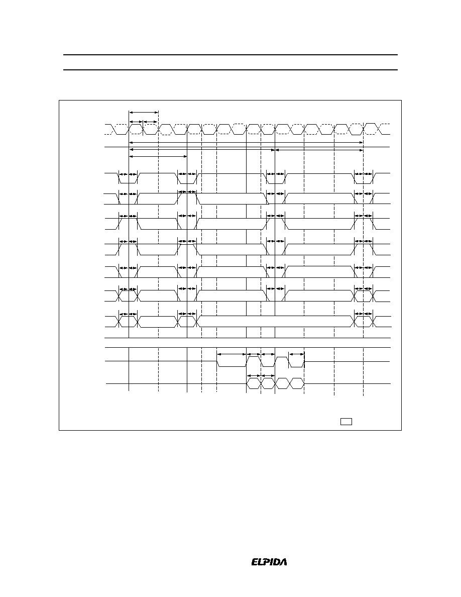
HM5425161B, HM5425801B, HM5425401B Series
Data Sheet E0086H20
57
Read Cycle
Bank 0
Active
Bank 0
Read
Bank 0
Precharge
;
;
;
;;
;
;
;
;;
;;
;
;
;;
;
;
;
;
CAS
latency = 2
Burst length = 4
Bank0 Access
= V
IH
or V
IL
;
Bank 0
Active
Bank 0
Read
Bank 0
Precharge
;
;
;
;
;
;;
;
;
;
;
;
;
;
;
;
;;
;
;
;
;
;
;
t
IS
t
IH
t
CH
t
CK
t
CL
t
IS
t
IH
t
IS
t
IH
t
IS
t
IH
t
IS
t
IH
t
IS
t
IH
t
IS
t
IH
t
IS
t
IH
t
IS
t
IH
t
IS
t
IH
t
IS
t
IH
t
IS
t
IH
t
IS
t
IH
t
IS
t
IH
t
IS
t
IH
t
IS
t
IH
t
IS
t
IH
t
IS
t
IH
t
IS
t
IH
t
IS
t
RPRE
t
RPST
t
DQSV
t
DQSV
t
DV
t
DV
t
IH
t
IS
t
IH
t
IS
t
IH
t
IS
t
IH
t
IS
t
IH
t
IS
t
IH
t
IS
t
IH
t
IS
t
IH
RAS
A10
Address
High-Z
High-Z
CS
CKE
CLK
CLK
CAS
WE
BA
DQS,
DQSU/DQSL
DQ (output)
DM,
DMU/DML
V
IH
t
RCD
t
RAS
t
RP
t
RC
;
;
;
;
;;
;
;
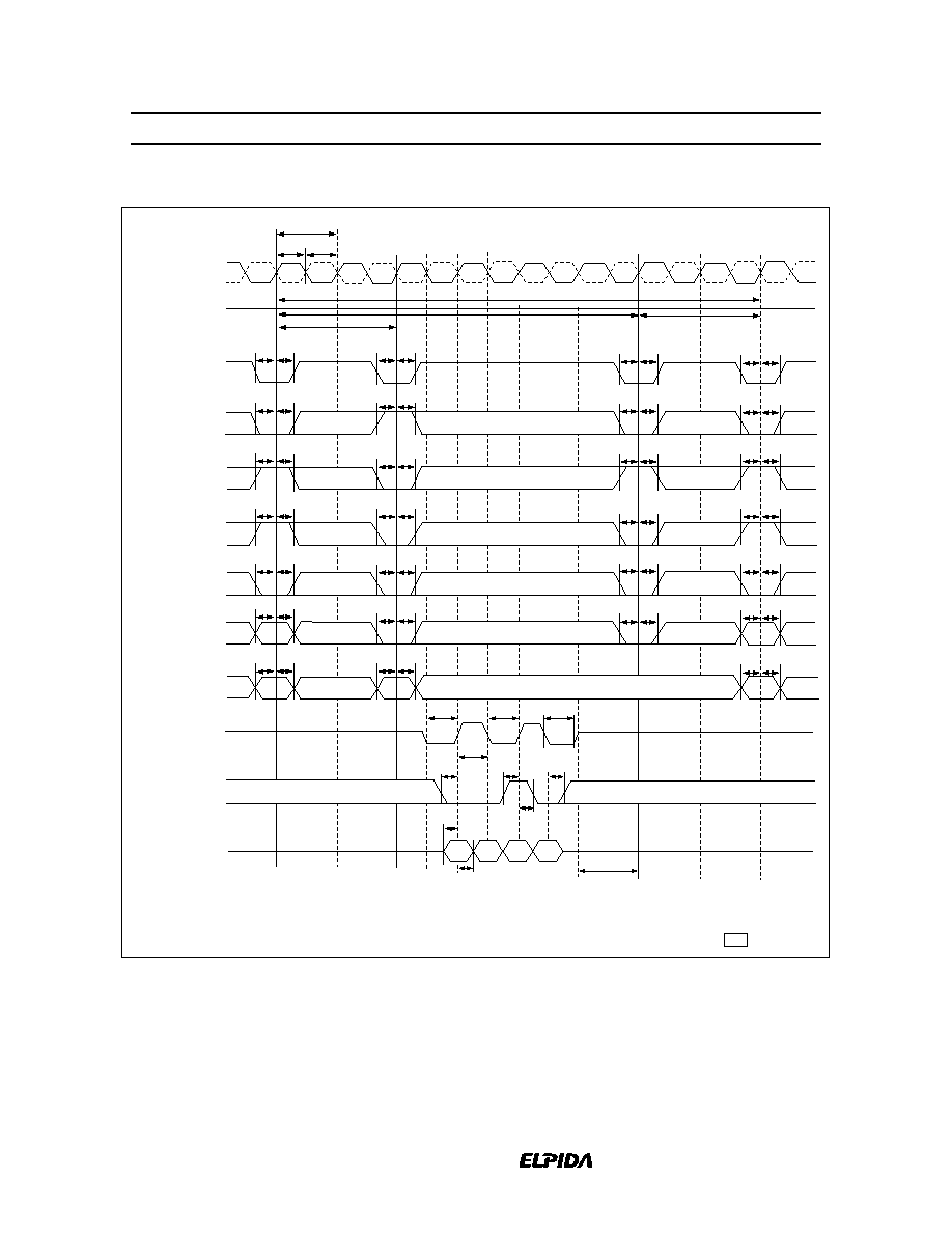
HM5425161B, HM5425801B, HM5425401B Series
Data Sheet E0086H20
58
Write Cycle
Bank 0
Active
;
;;
;
;
;
;
;
;
;
;
;
;
;;
;
CAS
latency = 2
Burst length = 4
Bank0 Access
= V
IH
or V
IL
;
;
Bank 0
Active
Bank 0
Write
Bank 0
Precharge
;
;
;
;
;
;
;
;
;
;
;
;
;
;
;
;
;;
;
;
;
;
;;
;
;
;
;
;
t
IS
t
IH
t
IS
t
IH
t
IS
t
IH
t
IS
t
IH
t
IS
t
IH
t
IS
t
IH
t
IS
t
IH
t
IS
t
IH
t
IS
t
IH
t
IS
t
IH
t
IS
t
IH
t
IS
t
IH
t
IS
t
IH
t
IS
t
IH
t
IS
t
IH
t
IS
t
IH
t
IS
t
IH
t
IS
t
IH
t
IS
t
IH
t
IS
t
IH
t
IS
t
IH
t
IS
t
IH
t
IS
t
IH
t
IS
t
IH
t
IS
t
IH
t
IS
t
IH
t
IS
t
IH
V
IH
t
RCD
t
RAS
t
RC
t
RP
t
DQSS
t
DQSL
t
DQSL
t
WPST
t
WR
CS
CLK
CLK
CKE
RAS
CAS
WE
BA
A10
Address
DQ (input)
DM,
DMU/DML
DQS,
DQSU/DQSL
(input)
t
CK
t
CH
t
CL
t
DS
t
DS
t
DS
t
DH
t
DH
t
DH
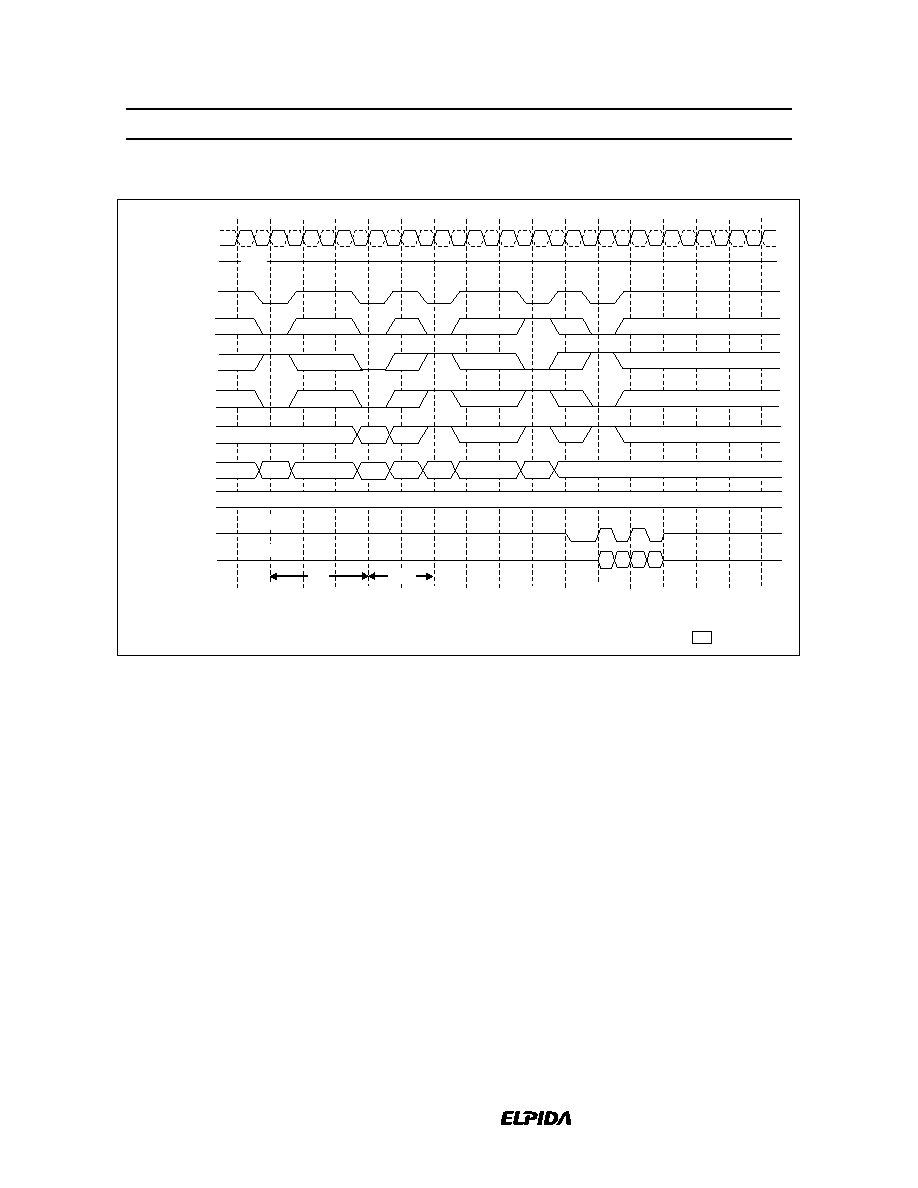
HM5425161B, HM5425801B, HM5425401B Series
Data Sheet E0086H20
59
Mode Register Set Cycle
0
1
2
3
4
5
6
7
8
9
10
11
12
13
14
15
CLK
CLK
CKE
CS
RAS
CAS
WE
BA
Address
DM,
DMU/DML
DQ (output)
;
;
;
;
;
;
;
;
;
;
;
;
;;
;;
;
;
;
;
b
valid
code
code
t
RP
Precharge
If needed
Mode
register
set
Bank 3
Active
Bank 3
Read
;
;
;
;
;
;
;
;
;
;
;
;
;
;
;
R: b
C: b
V
IH
Bank 3
Precharge
t
MRD
High-Z
High-Z
;
;
CAS
latency = 2
Burst length = 4
= V
IH
or V
IL
;;
DQS,
DQSU/DQSL
;;
;
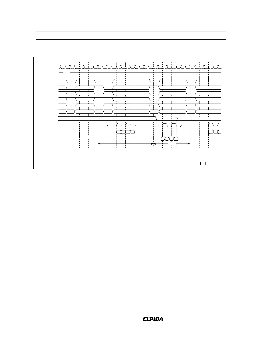
HM5425161B, HM5425801B, HM5425401B Series
Data Sheet E0086H20
60
Read/Write Cycle
;;
;
;
;
;
;
;
;
;
;
;
;
;
;;
R:a
C:a
C:b
R:b
C:b''
;
;
;
;
;;
;;
;
;
;
;
;
;
;
;
;
;
;
;
;
;
;;
b''
Bank 0
Active
Bank 3
Active
Bank 0
Read
Bank 3
Read
0
1
2
3
4
5
6
7
8
9
10
11
12
13
14
15
CKE
RAS
CS
DQS,
DQSU/DQSL
CAS
WE
Address
CLK
BA
DQ (output)
DQ (input)
CLK
Bank 3
Write
t
WRD
High-Z
V
IH
t
RWD
;
;
;
b
Read cycle
CAS
latency = 2
Burst lenght = 4
=V
IH
or V
IL
;
DM,
DMU/DML
;
;
;
a
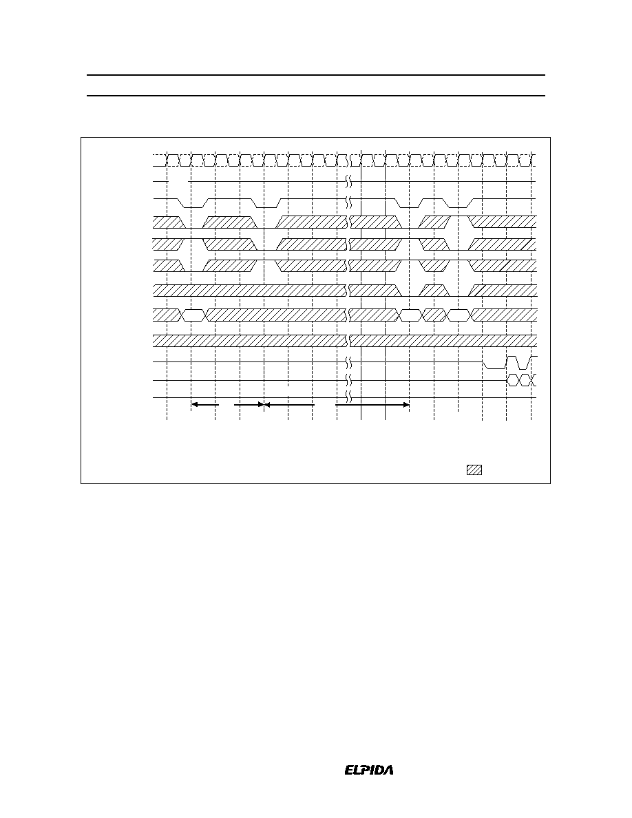
HM5425161B, HM5425801B, HM5425401B Series
Data Sheet E0086H20
61
Auto Refresh Cycle
Precharge
If needed
Auto
Refresh
Bank 0
Active
Bank 0
Read
CLK
CLK
CKE
CS
CAS
WE
BA
Address
DM,
DMU/DML
DQ (output)
DQ (input)
RAS
CAS
latency = 2
Burst length = 4
= V
IH
or V
IL
V
IH
t
RP
A10=1
R: b
C: b
b
High-Z
t
RFC
DQS
DQSU/DQSL
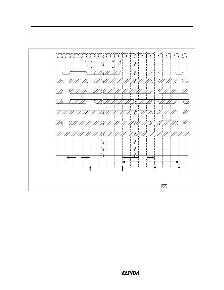
HM5425161B, HM5425801B, HM5425401B Series
Data Sheet E0086H20
62
Self Refresh Cycle
Self
refresh
entry
Self refresh
exit
High-Z
CLK
CKE
CS
RAS
CAS
WE
BA
Address
DM,
DMU/DML
DQ (output)
DQ (input)
CLK
Precharge
If needed
Bank 0
Active
Bank 0
Read
t
RP
t
SNR
A10=1
R: b
C: b
DQS
DQSU/DQSL
CAS
latency = 2.5
Burst length = 4
= V
IH
or V
IL
t
IS
t
IH
t
CKEPW
CKE = low
t
SRD
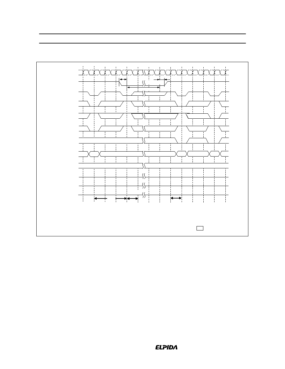
HM5425161B, HM5425801B, HM5425401B Series
Data Sheet E0086H20
63
Power Down Mode
;;
;
;
;
;
;
;
;
;;
;
;;
;;
;
;;
;
;;
;
;
;
;;
;
;
;
;;
;
;;
;;
;
;
;
;
;
;
;
;
;
;
;
;
;
;
;;
;;
;;
;;
;
;
;
;
;
;
;
;;
;;
;
;;
;
;
High-Z
A10=1
R: c
R: b
CLK
CKE
CS
RAS
CAS
WE
BA
Address
DM,
DMU/DML
DQ (output)
DQ (input)
QS,
QSU/QSL
CLK
Precharge
If needed
Power down
entry
Power
down
exit
Bank 0
Active
Bank 0
Read
t
PDEX
CAS
latency = 2.5
Burst lenght = 4
=V
IH
or V
IL
;
t
PDEN
CKE = low
;
;;
;
;;
;
;;
t
RP
t
IS
t
IH
t
CKEPW
HM5425161B, HM5425801B, HM5425401B Series
Data Sheet E0086H20
64
Package Dimensions
HM5425161BTT/HM5425801BTT/HM5425401BTT Series
0.10
0.65
66
34
1
33
22.22 ± 0.10
1.0 ± 0.05
1.20 max
10.16
0 to 8
∞
0.91 max.
0.09 to 0.20
0.17 to 0.32
0.10
0.60 ± 0.15
0.80
Nom
0.25
+0.08
-
0.05
11.76
±
0.20
ECA-TS2-0029-01
Note: This dimension does not include mold flash, protrusions or gate burrs. Mold flash, protrusions or
gate burrs shall not exceed 0.20mm per side.
A
PIN#1 ID
S
0.13
M S A B
Unit: mm
B
*
1
S
HM5425161B, HM5425801B, HM5425401B Series
Data Sheet E0086H20
65
Cautions
1. Elpida Memory, Inc. neither warrants nor grants licenses of any rights of Elpida Memory, Inc.'s or any
third party's patent, copyright, trademark, or other intellectual property rights for information contained in
this document. Elpida Memory, Inc. bears no responsibility for problems that may arise with third party's
rights, including intellectual property rights, in connection with use of the information contained in this
document.
2. Products and product specifications may be subject to change without notice. Confirm that you have
received the latest product standards or specifications before final design, purchase or use.
3. Elpida Memory, Inc. makes every attempt to ensure that its products are of high quality and reliability.
However, contact Elpida Memory, Inc. before using the product in an application that demands especially
high quality and reliability or where its failure or malfunction may directly threaten human life or cause
risk of bodily injury, such as aerospace, aeronautics, nuclear power, combustion control, transportation,
traffic, safety equipment or medical equipment for life support.
4. Design your application so that the product is used within the ranges guaranteed by Elpida Memory, Inc.
particularly for maximum rating, operating supply voltage range, heat radiation characteristics, installation
conditions and other characteristics. Elpida Memory, Inc. bears no responsibility for failure or damage
when used beyond the guaranteed ranges. Even within the guaranteed ranges, consider normally
foreseeable failure rates or failure modes in semiconductor devices and employ systemic measures such as
fail-safes, so that the equipment incorporating Elpida Memory, Inc. product does not cause bodily injury,
fire or other consequential damage due to operation of the Elpida Memory, Inc. product.
5. This product is not designed to be radiation resistant.
6. No one is permitted to reproduce or duplicate, in any form, the whole or part of this document without
written approval from Elpida Memory, Inc..
7. Contact Elpida Memory, Inc. for any questions regarding this document or Elpida Memory, Inc.
semiconductor products.
© Hitachi, Ltd., 2000