Äîêóìåíòàöèÿ è îïèñàíèÿ www.docs.chipfind.ru

Document No. E0039N30 (Ver. 3.0)
Date Published July 2002 (K) Japan
URL: http://www.elpida.com
Elpida Memory, Inc. 2001-2002
NEC Corporation 2000
Elpida Memory, Inc. is a joint venture DRAM company of NEC Corporation and Hitachi, Ltd.
DATA SHEET
288M bits Direct Rambus DRAM
µ
µ
µ
µ
PD488588 (512K words
×
×
×
×
18 bits
×
×
×
×
32s banks)
Description
The Direct Rambus DRAM (Direct RDRAM) is a
general purpose high-performance memory device
suitable for use in a broad range of applications
including computer memory, graphics, video, and any
other application where high bandwidth and low
latency are required.
The
µ
PD488588 is 288Mbits Direct Rambus DRAM
(RDRAM
), organized as 16M words by 18 bits.
The use of Rambus Signaling Level (RSL) technology
permits 600MHz to 800MHz transfer rates while using
conventional system and board design technologies.
Direct RDRAM devices are capable of sustained data
transfers at 1.25ns per two bytes (10ns per sixteen
bytes).
The architecture of the Direct RDRAMs allows the
highest sustained bandwidth for multiple, simultaneous
randomly addressed memory transactions.
The separate control and data buses with independent
row and column control yield over 95% bus efficiency.
The Direct RDRAM's four banks support up to four
simultaneous transactions.
System oriented features for mobile, graphics and
large memory systems include power management,
byte masking.
The
µ
PD488588 is offered in a CSP horizontal
package suitable for desktop as well as low-profile
add-in card and mobile applications. Direct RDRAMs
operate from a 2.5V
supply.
Features
·
Highest sustained bandwidth per DRAM device
-- 1.6 GB/s sustained data transfer rate
-- Separate control and data buses for maximized
efficiency
-- Separate row and column control buses for easy
scheduling and highest performance
-- 32 banks: four transactions can take place
simultaneously at full bandwidth data rates
·
Low latency features
-- Write buffer to reduce read latency
-- 3 precharge mechanisms for controller flexibility
-- Interleaved transactions
·
Advanced power management:
-- Multiple low power states allows flexibility in power
consumption versus time to active state
-- Power-down self-refresh
·
Overdrive current mode
·
Organization: 2K bytes pages and 32 banks, x 18
·
Uses Rambus Signaling Level (RSL) for up to
800MHz operation
·
Package : 80-ball FBGA (
µ
BGA
)
(17.16
×
10.2)

Data Sheet
E0039N30 (Ver. 3.0)
2
µ
µ
µ
µ
PD488588
Ordering Information
Part number
Organization*
words
×
bits
×
Internal
Banks
Clock frequency
MHz (max.)
/RAS access
time (ns)
Package
µ
PD488588FF-C60-53-DH1
512K x 18 x 32s
600
53
80-ball FBGA (
µ
BGA)
µ
PD488588FF-C71-45-DH1
711
45
(17.16
×
10.2)
µ
PD488588FF-C80-45-DH1
800
45
Note: The "32s" designation indicates that this RDRAM core is composed of 32 banks which use a "split" bank
architecture
Data Sheet
E0039N30 (Ver. 3.0)
3
µ
µ
µ
µ
PD
488588
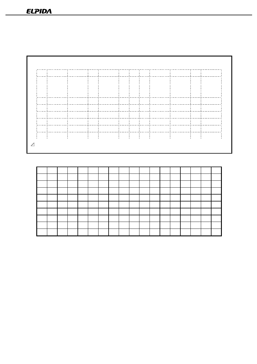
Pin Configuration
80-ball FBGA (
µ
µ
µ
µ
BGA)
(17.16
×
×
×
×
10.2)
Top View
10
O O
O
O
9
8
O O O O O O O O O O O O O O O O O O
7
O O O O O O O O O O O O O O O O O O
6
5
4
O O O O O O O O O O O O O O O O O O
3
O O O O O O O O O O O O O O O O O O
2
1
O O
O
O
A B C D E F G H J K L M N P R S T U
10
V
DD
GND
GND
V
DD
9
8
GND
V
DD
CMD
V
DD
GND GNDa GNDa
V
DD
V
DD
GND GND
V
DD
V
DD
GND GND
VCMOS
V
DD
GND
7
V
DD
DQA8 DQA7 DQA5 DQA3 DQA1 CTMN CTM ROW2 ROW0 COL3 COL1 DQB1 DQB3 DQB5 DQB7 DQB8
V
DD
6
5
4
GND GND DQA6 DQA4 DQA2 DQA0 CFM CFMN ROW1 COL4 COL2 COL0 DQB0 DQB2 DQB4 DQB6 GND GND
3
V
DD
GND SCK
VCMOS
GND
V
DD
GND
V
DD
a
V
REF
GND
V
DD
GND GND
V
DD
SIO0 SIO1 GND
V
DD
2
1
V
DD
GND
GND
V
DD
A B C D E F G H J K L M N P R S T U
Note Some signals can be applied because this pin is not connected to the inside of the chip.
Data Sheet
E0039N30 (Ver. 3.0)
4
µ
µ
µ
µ
PD488588
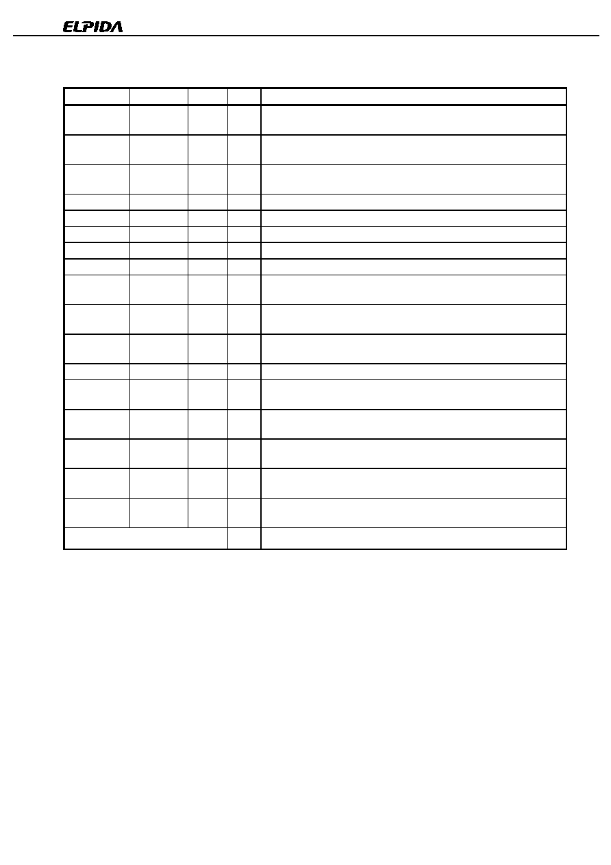
Pin Description
Signal
Input / Output
Type
#pins
Description
SIO0, SIO1
Input / Output CMOS
Note1
2
Serial input/output. Pins for reading from and writing to the control registers using
a serial access protocol. Also used for power management.
CMD Input
CMOS
Note1
1
Command input. Pins used in conjunction with SIO0 and SIO1 for reading from
and writing to the control registers. Also used for power management.
SCK Input
CMOS
Note1
1
Serial clock input. Clock source used for reading from and writing to the control
registers.
V
DD
18
Supply voltage for the RDRAM core and interface logic.
V
DDa
1
Supply voltage for the RDRAM analog circuitry.
V
CMOS
2
Supply voltage for CMOS input/output pins.
GND
22
Ground reference for RDRAM core and interface.
GND
a
2
Ground reference for RDRAM analog circuitry.
DQA8..DQA0
Input / Output RSL
Note2
9
Data byte A. Nine pins which carry a byte of read or write data between the
Channel and the RDRAM.
CFM Input
RSL
Note2
1
Clock from master. Interface clock used for receiving RSL signals from the
Channel. Positive polarity.
CFMN Input
RSL
Note2
1
Clock from master. Interface clock used for receiving RSL signals from the
Channel. Negative polarity.
V
REF
1
Logic threshold reference voltage for RSL signals.
CTMN Input
RSL
Note2
1
Clock to master. Interface clock used for transmitting RSL signals to the Channel.
Negative polarity.
CTM Input
RSL
Note2
1
Clock to master. Interface clock used for transmitting RSL signals to the Channel.
Positive polarity.
ROW2..ROW0 Input RSL
Note2
3
Row access control. Three pins containing control and address information for
row accesses.
COL4..COL0 Input
RSL
Note2
5
Column access control. Five pins containing control and address information for
column accesses.
DQB8..DQB0
Input / Output RSL
Note2
9
Data byte B. Nine pins which carry a byte of read or write data between the
Channel and the RDRAM.
Total pin count per package
80
Notes 1. All CMOS signals are high-true ; a high voltage is a logic one and a low voltage is logic zero.
2. All RSL signals are low-true ; a low voltage is a logic one and a high voltage is logic zero.
Data Sheet
E0039N30 (Ver. 3.0)
5
µ
µ
µ
µ
PD
488588
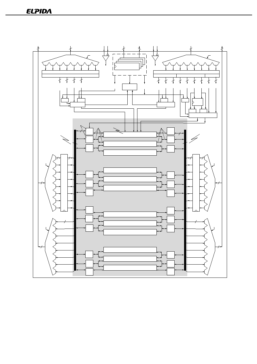
Block Diagram
11
5
5
9
ROP
AV
DR
BR
R
C
MB
MA
COP
S
DC
BC
XOP
M
DX
BX
Packet Decode
Control Registers
DEVID
REFR
PRER
PREX
PREC
RD, WR
ACT
DM
ROWR
ROWA
Packet Decode
COLM
COLC
COLX
1:8 Demux
RCLK
RQ7..RQ5 or
ROW2..ROW0
3
SCK, CMD
2
SIO0, SIO1
2
1:8 Demux
RCLK
RQ4..RQ0 or
COL4..COL0
5
TCLK
CTM
DQB8..DQB0
DQA8..DQA0
CTMN
RCLK
CFM CFMN
Power Modes
RCLK
TCLK
1:8 Demux
Write Buffer
9
8:1 Mux
9
TCLK
8:1 Mux
9
RCLK
1:8 Demux
Write Buffer
Write
Buffer
Bank 0
Bank 1
Bank 2
Bank 13
Bank 14
Bank 15
Bank 16
Bank 17
Bank 18
Bank 29
Bank 30
Bank 31
SAmp
0
9
9
9
9
9
9
72
72
72
Internal DQA Data Path
Internal DQB Data Path
Sense Amp
64x72
64x72
DRAM Core
512x128x144
72
9
Column Decode & Mask
Match
Match
Match
XOP Decode
Mux
Row Decode
9
9
Mux
Mux
SAmp
0/1
SAmp
1/2
SAmp
13/14
SAmp
14/15
SAmp
15
SAmp
16
SAmp
16/17
SAmp
17/18
SAmp
29/30
SAmp
30/31
SAmp
31
SAmp
31
SAmp
30/31
SAmp
29/30
SAmp
17/18
SAmp
16/17
SAmp
16
SAmp
15
SAmp
14/15
SAmp
13/14
SAmp
1/2
SAmp
0/1
SAmp
0
64x72
6
5
5
5
5
5
7
8
8
·
·
·
·
·
·
·
·
·
·
·
·
·
·
·
·
·
·
Document Outline
- COVER
- Description
- Features
- Ordering Information
- Pin Configuration
- Pin Description
- Block Diagram
- 1. General Description
- 2. Packet Format
- 3. Field Encoding Summary
- 4. DQ Packet Timing
- 5. COLM Packet to D Packet Mapping
- 6. ROW-to-ROW Packet Interaction
- 7. ROW-to-COL Packet Interaction
- 8. COL-to-COL Packet Interaction
- 9. COL -to-ROW Packet Interaction
- 10. ROW-to-ROW Examples
- 11. Row and Column Cycle Description
- 12. Precharge Mechanisms
- 13. Read Transaction - Example
- 14. Write Transaction - Example
- 15. Write/Retire - Examples
- 16. Interleaved Write - Example
- 17. Interleaved Read - Example
- 18. Interleaved RRWW - Example
- 19. Control Register Transactions
- 20. Control Register Packets
- 21. Initialization
- 22. Control Register Summary
- 23. Power State Management
- 24. Refresh
- 25. Current and Temperature Control
- 26. Electrical Conditions
- 27. Timing Conditions
- 28. Electrical Characteristics
- 29. Timing Characteristics
- 30. RSL Clocking
- 31. RSL - Receive Timing
- 32. RSL - Transmit Timing
- 33. CMOS - Receive Timing
- 34. CMOS - Transmit Timing
- 35. RSL - Domain Crossing Window
- 36. Timing Parameters
- 37. Absolute Maximum Ratings
- 38. IDD - Supply Current Profile
- 39. Capacitance and Inductance
- 40. Interleaved Device Mode
- 41. Glossary of Terms
- 42. Package Drawing
- 43. Recommended Soldering Conditions