 | –≠–ª–µ–∫—Ç—Ä–æ–Ω–Ω—ã–π –∫–æ–º–ø–æ–Ω–µ–Ω—Ç: eKK6511Q | –°–∫–∞—á–∞—Ç—å:  PDF PDF  ZIP ZIP |
Preliminary
eKK6511
RF KEYBOARD ENCODER
* This specification are subject to be changed without notice.
1
2002/11/15
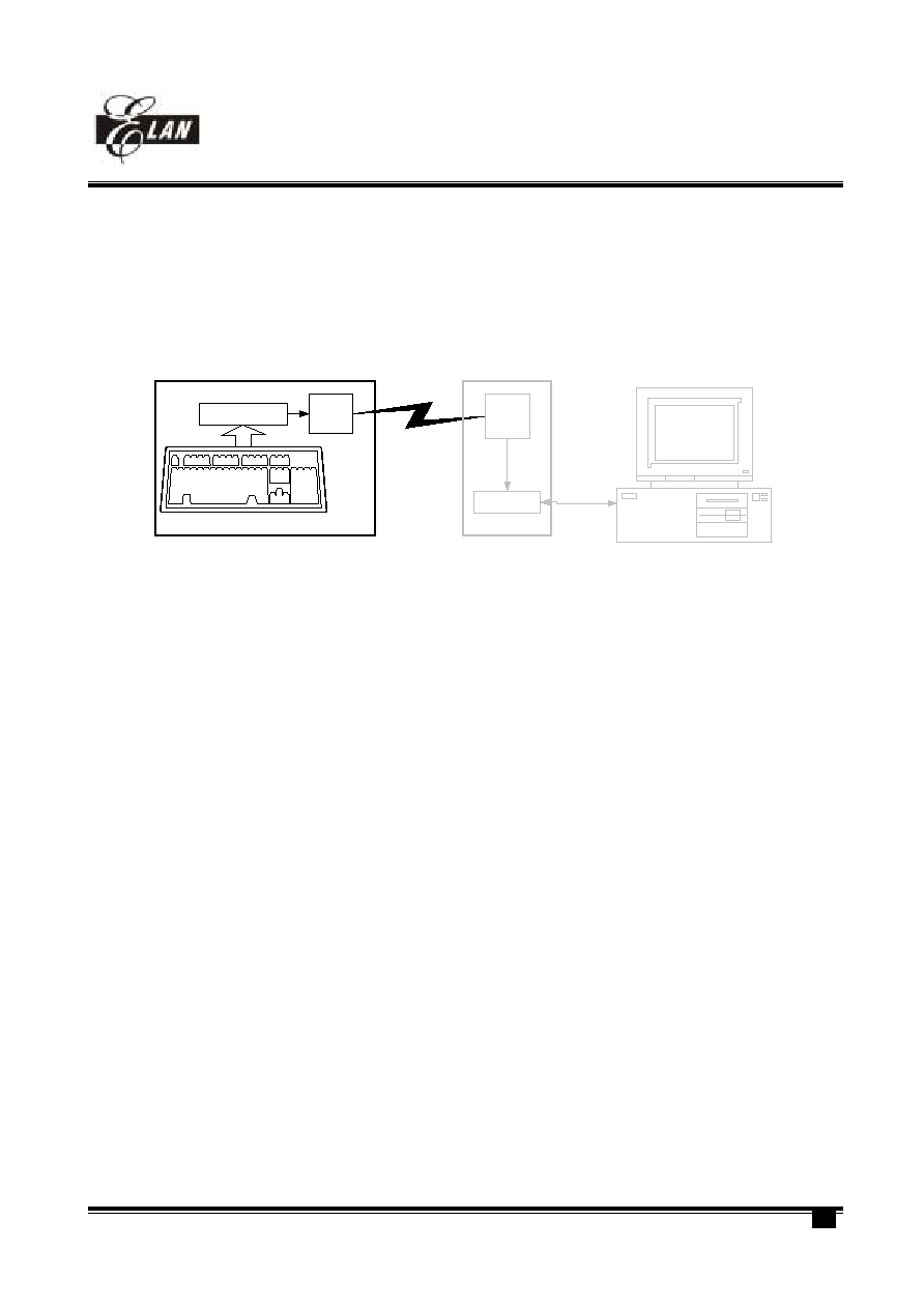
GENERAL DESCRIPTION
In RF keyboard system, that is divided into two parts (the transmitter and the receiver). The eKK6511
micro-controller is dedicated to a RF keyboard encoder for single channel RF transmitter module. The eKK6511 is
scanning keyboard state, encode key data and rely on RF Tx module to transmit data.
RF Tx
Module
Keyboard
RF Rx
Module
eKK6111
IBM Compatible
Receiver
PS/2
eKK6511
Transmitter
RF
FEATURES
Low cost ≠ eliminate need external components.
Phantom key detect.
Resonator oscillator (2.00 MHz)
Low power CMOS device technology
Internal pull-up resistor.
Tri-state outputs for easy board application.
Built-in 4K ROM.
Support WINDOWS
TM
95, 98, 2000 keys.
104/107 keys with multi-media or other special keyboard encoder.
Support RF transmit module sleep mode (Sleep current under 10µA).
Warm-up time of RF Tx modules: 7.2µ sec
Using the device ID to identify which receiver was connected.
-
DIP switch to select. (8 sets ID)
-
Random generate ID (255 sets ID) and store in EEPROM (93LC46)
Package: 40-pins PDIP, 44-pins QFP
APPLICATION
Support the single channel or two channels RF transmitter module.
IBM PC AT or compatible machine keyboard.
IBM PS/2 model 30,50,60,80 or compatible machine keyboard.
Japanese keyboard.
Korean keyboard.
Brazilian keyboard.
European keyboard.
Preliminary
Symbol
I / O
Function
P50
O
Column 3 Low output scan line, 3-state
P51
O
Column 4 Low output scan line, 3-state
P52
O
Column 5 Low output scan line, 3-state
P53
O
Column 6 Low output scan line, 3-state
P54
O
Column 7 Low output scan line, 3-state
P55
O
Column 14 Low output scan line, 3-state
P56
O
Column 13 Low output scan line, 3-state
P57
O
Column 12 Low output scan line, 3-state
P80
O
Column 11 Low output scan line, 3-state
P81
O
Column 15 Low output scan line, 3-state
P82
O
Column 10 Low output scan line, 3-state
P83
O
Column 8 Low output scan line, 3-state
P84
O
Column 9 Low output scan line, 3-state
P85
O
Column 0 Low output scan line, 3-state
P86
O
Column 16 Low output scan line, 3-state
P87
O
Column 17 Low output scan line, 3-state
P91
O
Switch DIP control line or Random ID connect bottom
P90
I
Switch DIP for Device ID bit 2 or connect with DO pin of EEPROM
P70
O
Connect with CS pin of EEPROM
P74
I / O
Switch DIP for Device ID bit 1 or connect with SK pin of EEPROM
P75
I / O
Switch DIP for Device ID bit 0 or connect with DI pin of EEPROM
P92
O
Control line for RF Transmitter Module
P93
O
Data Output for RF Transmitter Module connection
P94
O
Column 1 Low output scan line, 3-state
P95
O
Column 2 Low output scan line, 3-state
VSS I
Ground
P60
I
Row 0 Input Scan line, internal pull high (17K)
P61
I
Row 1 Input Scan line, internal pull high (17K)
P62
I
Row 2 Input Scan line, internal pull high (17K)
P63
I
Row 3 Input Scan line, internal pull high (17K)
P64
I
Row 4 Input Scan line, internal pull high (17K)
P65
I
Row 5 Input Scan line, internal pull high (17K)
P66
I
Row 6 Input Scan line, internal pull high (17K)
P67
I
Row 7 Input Scan line, internal pull high (17K)
eKK6511
RF KEYBOARD ENCODER
* This specification are subject to be changed without notice.
2
2002/11/15
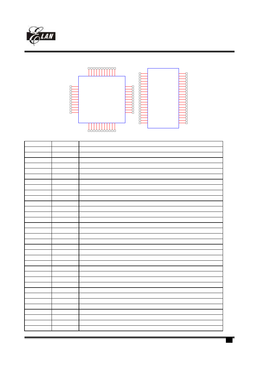
PIN ASSIGNMENT
eKK6511Q
U1
1
2
3
4
5
6
7
8
9
10
11
12 13 14 15 16 17 18 19 20
22
21
33
32
31
30
29
28
27
26
25
24
23
44 43 42 41 40 39 38 37 36 35 34
DO/ID2
CONN
RFC
TXD
C1
C2
C3
C4
C5
C6
C7
C14 C13 C12 C11 C15 NC C10 C8 C9
C16
C0
NC
NC
R7
R6
R5
R4
R3
R2
R1
R0
C17
SK/ID1 DI/ID0
/INT VSS
O
SCO
R-O
SCI VDD NC NC NC
CS
U2
eKK6511P
1
2
3
4
5
6
7
8
9
10
11
12
13
14
15
16
17
18
19
20
40
39
38
37
36
35
34
33
32
31
30
29
28
27
26
25
24
23
22
21
VSS
/INT
DI/ID0
SK/ID1
DO/ID2
CONN
RFC
TXD
C1
C2
C3
C4
C5
C6
C7
C14
C13
C12
C11
C15
OSCO
R-OSCI
VDD
CS
NC
NC
R7
R6
R5
R4
R3
R2
R1
R0
C17
C16
C0
C9
C8
C10
PIN DESCRIPTIONS
eKK6511
RF KEYBOARD ENCODER
* This specification are subject to be changed without notice.
3
2002/11/15
Preliminary
VDD
I
+3V Battery power supply
OSCO O
CLOCK
output
OSCI
I
Connect with 2.00MHz Resonator Oscillation
FUNCTION DESCRIPTION
Encoder buffer
The eKK6511 will buffer 24 bytes first-in-first-out order when the system is able to receive scan codes from the
keyboard. The eKK6511 generate RF data frame according to FIFO and keyboard status. Then, modulation the data
frame into serial signal to RF Tx module. When key pressed, the EKK6511 will generate a make code into FIFO. If key
not released, eKK6511 will generate a make code into FIFO every 200ms. When key released, the eKK6511 will
generate a break code into FIFO.
Device ID
The eKK6511 has support two device ID mode:
1. Controllable ID mode: Using the 3 bits DIP switch to control the device ID.
2. Random generate ID mode: Using the push bottom to generates a random device ID (255 sets) and restores in
EEPROM (93LC46). The eKK6511 will broadcast 10 seconds the new device ID after push bottom released. When
battery exchange or reset, the device ID will recovery from EEPROM.
ABSOLUTE MAXIMUM RATINGS
Parameter
Sym.
Ratings
Temperature under bias
T
OPR
0 to 70
Storage temperature
T
STR
-65 to 150
Input Voltage
V
IN
-0.3V to +6V
Output Voltage
V
OUT
-0.3V to +6V
DC ELECTRICAL CHARACTERISTICS
Symbol
Parameter
Condition
Min.
Typ.
Max.
Unit
I
IL
Input Leakage current
V
IN
=V
DD
, V
SS
±1
mA
V
IH
Input
High
Voltage
2.0
V
V
IL
Input
Low
Voltage
0.8 V
V
IHX
Clock Input High voltage
OSCI
3.5
V
V
ILX
Clock Input Low voltage
OSCI
1.5
V
V
OH1
Output High voltage
(Ports 5,6,8,9 and P74,P75)
I
OH
=-12.0mA 2.4
V
V
OH2
Output High voltage
(P70~P72)(S7=0)
I
OH
=-10.0mA
2
V
V
OH3
Output High Voltage
(P70~P72)(S7=0)
I
OH
=-10.0mA 2.4
V
V
OL1
Output Low Voltage
(ports 5,6,8,9 and P74~P75)
I
OL
=5.0mA
0.4
V
V
OL2
Output Low voltage
(P70~P72)(S7=0)
I
OL
=12.0mA
0.4
V
V
OL3
Output Low Voltage
(P70~P72)(S7=1)(P76~P77)
I
OL
=10.0mA
3
V
I
PH
Pull-high current
Pull-high active, input pin at V
SS
-250 -400 -500 µA
I
SB
Power-down
current
All input and I/O pin at V
DD
,
output pin floating, WDT enabled
10
mA
Preliminary
eKK6511
RF KEYBOARD ENCODER
* This specification are subject to be changed without notice.
4
2002/11/15
I
CC1
Operating supply current
(V
DD
=5.0V) at two cycles/two
clocks
/RESET=High
Fosc=2.00Mhz(CK2="0"), output
pin floating
3
mA
AC ELECTRICAL CHARACTERISTIC(Ta=0
~70
, VDD=5V, VSS=0V)
Symbol
Parameter
Condition
Min.
Typ.
Max.
Unit
D
CLK
Input CLK duty cycle
45
50
55
%
T
TCC
TCC input period
(Tins+20)/N
ns
T
WDT
Watchdog timer period
Ta=25
18
ns
T
DRH
Device reset hold period
Ta=25
18
ns
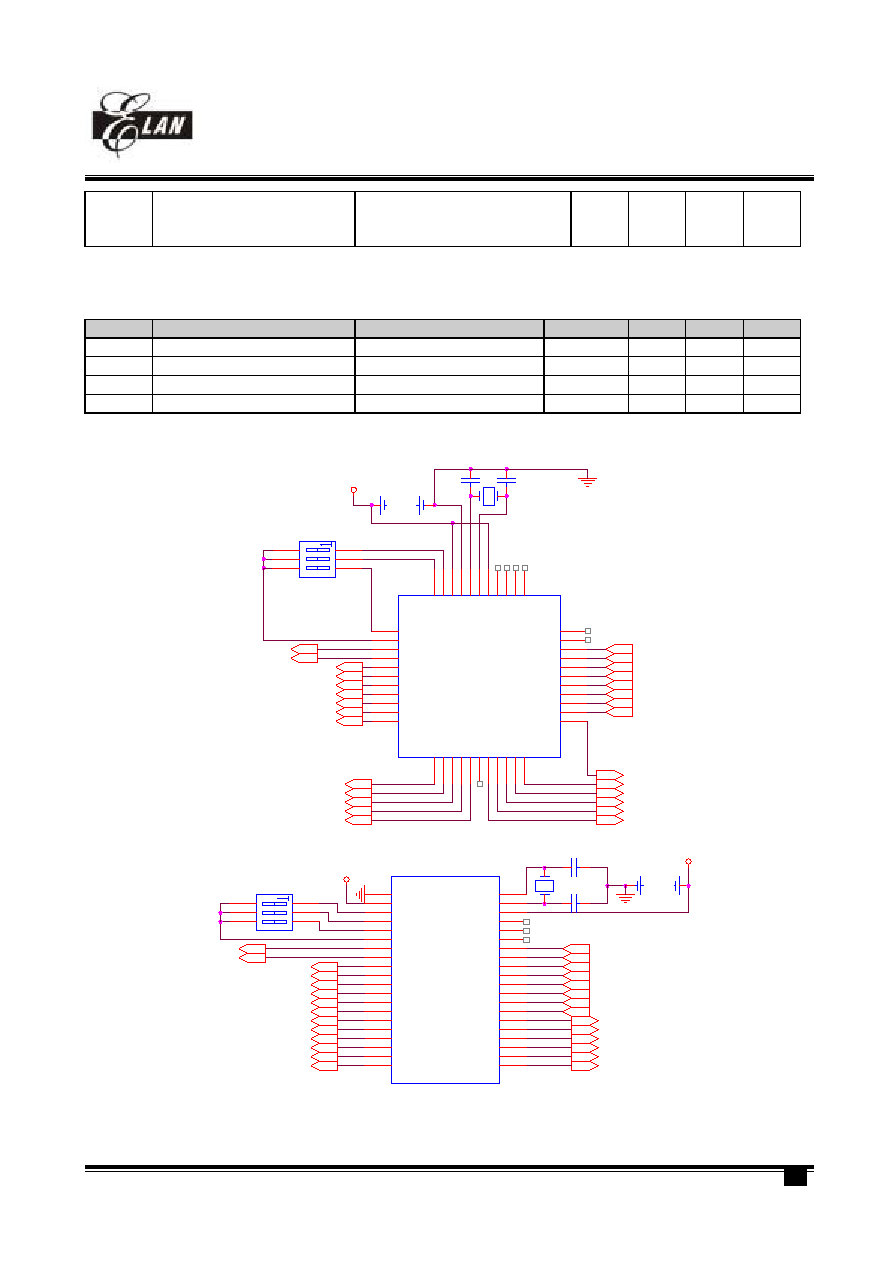
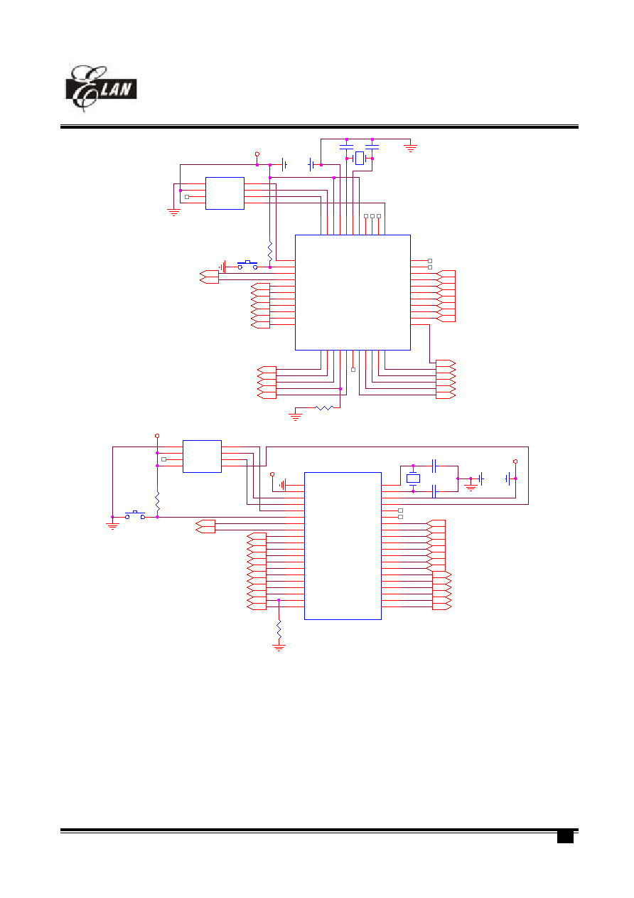
APPLICATION CIRCUIT
S1
S3
eKK6511Q
U5
1
2
3
4
5
6
7
8
9
10
11
12 13 14 15 16 17 18 19 20
22
21
33
32
31
30
29
28
27
26
25
24
23
44 43 42 41 40 39 38 37 36 35 34
DO/ID2
CONN
RFC
TXD
C1
C2
C3
C4
C5
C6
C7
C14 C13 C12 C11 C15 NC C10 C8 C9
C16
C0
NC
NC
R7
R6
R5
R4
R3
R2
R1
R0
C17
SK/ID1 DI/ID0
/INT VSS
O
SCO
R-O
SCI VDD NC NC NC
CS
S16
S17
R5
S5
RF Control
S11
S14
S4
SW3
Device ID
20pF
S2
R1
VCC
S7
S15
R4
R3
S10
20pF
2.00Mhz
R2
S6
S0
--
-
Battery(1.5Vx2)
S13
R0
R7
R6
RF Data
S12
S8
S9
S13
S1
S15
S4
S10
VCC
S2
S16
R7
S5
S7
S6
20pF
2.00MHz
R1
S17
RF Control
SW3
Device ID
S3
20pF
- - -
BATTERY(1.5Vx2)
R3
S12
R4
S0
S8
RF Data
VCC
S9
R6
S11
R2
U4
eKK6511P
1
2
3
4
5
6
7
8
9
10
11
12
13
14
15
16
17
18
19
20
40
39
38
37
36
35
34
33
32
31
30
29
28
27
26
25
24
23
22
21
VSS
/INT
DI/ID0
SK/ID1
DO/ID2
CONN
RFC
TXD
C1
C2
C3
C4
C5
C6
C7
C14
C13
C12
C11
C15
OSCO
R-OSCI
VDD
CS
NC
NC
R7
R6
R5
R4
R3
R2
R1
R0
C17
C16
C0
C9
C8
C10
S14
R5
R0
DIP Switch ID mode
Preliminary
eKK6511
RF KEYBOARD ENCODER
* This specification are subject to be changed without notice.
5
2002/11/15
RF Control
VCC
S13
R4
R5
R7
20pF
S3
R6
S9
20pF
2.00Mhz
R0
R1
S4
100Kohm
S0
S10
U3
93C46
1
2
3
4
8
7
6
5
CS
SK
DI
DO
VCC
DC
ORG
GND
--
-
Battery(1.5Vx2)
S17
S2
S7
S14
R2
RF Data
CONNECT
560Kohm
R3
S1
S11
S16
eKK6511Q
U5
1
2
3
4
5
6
7
8
9
10
11
12 13 14 15 16 17 18 19 20
22
21
33
32
31
30
29
28
27
26
25
24
23
44 43 42 41 40 39 38 37 36 35 34
DO/ID2
CONN
RFC
TXD
C1
C2
C3
C4
C5
C6
C7
C14 C13 C12 C11 C15 NC C10 C8 C9
C16
C0
NC
NC
R7
R6
R5
R4
R3
R2
R1
R0
C17
SK/ID1 DI/ID0
/INT VSS
O
SCO
R-O
SCI VDD NC NC NC
CS
S5
S12
S8
S15
S6
560Kohm
U3
eKK6511P
1
2
3
4
5
6
7
8
9
10
11
12
13
14
15
16
17
18
19
20
40
39
38
37
36
35
34
33
32
31
30
29
28
27
26
25
24
23
22
21
VSS
/INT
DI/ID0
SK/ID1
DO/ID2
CONN
RFC
TXD
C1
C2
C3
C4
C5
C6
C7
C14
C13
C12
C11
C15
OSCO
R-OSCI
VDD
CS
NC
NC
R7
R6
R5
R4
R3
R2
R1
R0
C17
C16
C0
C9
C8
C10
S12
S1
R5
S2
S7
S16
R2
560Kohm
S4
93C46
1
2
3
4
8
7
6
5
CS
SK
DI
DO
VCC
DC
ORG
GND
S15
R1
S11
- - -
BATTERY(1.5Vx2)
S9
R3
CONNECT
S0
S17
R7
R4
S14
2.00MHz
20pF
VCC
S8
S10
VCC
R6
S13
VCC
S6
20pF
RF Control
S3
S5
R0
RF Data
Random generate ID mode