1
* This specification are subject to be changed without notice.
EM19100
8-BIT 20 MSPS VIDEO A/D CONVERTER (CMOS)
1.26.1996
GENERAL DESCRIPTION
EM19100 is an 8-bit CMOS A/D converter for video use. The adoption of a 2-step parallel system achieves low
consumption at a maximum conversion speed of 20 MSPS typical.
FEATURES
∑ 20MSPS maximum conversion speed
∑ Build-in sampling and hold circuit
∑ Internal self-bias reference voltage
∑ 90mW power dissipation at 20MSPS
∑ +5V single power supply
∑ Available in 24 pin SOP
∑ Series
EM19100M for 300 mil SOP
EM19100S for 209 mil SOP
APPLICATION
TV,VCR digital systems and a wide range of fields where high speed A/D conversion is required.
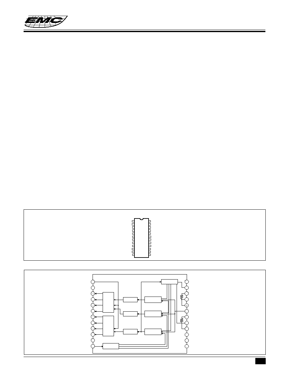
PIN ASSIGNMENT
EM19100
8-BIT 20 MSPS VIDEO A/D CONVERTER (CMOS)
Lower data
latches
Upper data
latches
Lower encoder
(4bit)
Upper encoder
(4bit)
Lower encoder
(4bit)
Lower
Comparators with
S/ H (4bit)
Upper
Comparators with
S/ H (4bit)
Lower
Comparators with
S/ H (4bit)
Reference voltage
4
3
6
5
8
7
1 0
9
1 2
1 1
2
1
1 5
1 3
1 4
1 6
1 7
1 8
1 9
2 0
2 1
2 2
2 3
2 4
Clock generator
/ O E
DVS S
D 0
D 1
D 2
D 3
D 4
D 5
D 6
D 7
DV DD
CL K
DV DD
AV DD
AV DD
V RT S
V RT
AV DD
VI N
AVSS
V RBS
V R B
AVSS
DV S S
FUNCTIONAL BLOCK DIAGRAM
1
2
3
4
5
6
7
8
9
10
11
12
24
23
22
21
20
19
18
17
16
15
14
13
OE
DVSS
D0
D1
D2
D3
D4
D5
D6
D7
DVDD
CLK
DVSS
VRB
VRBS
AVSS
AVSS
VIN
AVDD
VRT
VRTS
AVDD
AVDD
DVDD
EM19100

* This specification are subject to be changed without notice.
EM19100
8-BIT 20 MSPS VIDEO A/D CONVERTER (CMOS)
4
1.26.1996
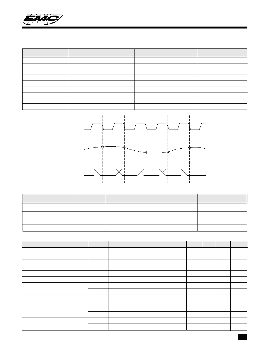
Timing explanation
EM19100 is a 2-step parallel system A/D converter featuring a 4-bit upper comparators group and 2 lower
comparators groups of 4-bit each. The reference voltage that is equal to the voltage between V
RT
-V
RB
/16 is
constantly applied to the upper 4-bit comparator block. Voltage that corresponded to the upper data is fed through
the reference supply to the lower data. V
RTS
and V
RBS
pins serve for the self generation of V
RT
(Reference
voltage top) and V
RB
(Reference voltage bottom).
This IC uses an offset cancel type comparator and operates synchronously with an external clock. It features the
following operating modes which are respectively indicated on the timing chart with S, H, C symbols. That is
input sampling (auto zero) mode, input hold mode and comparison mode.
The operation of respective parts is as indicated in the chart. For instance input voltage Vi(1) is sampled with the
falling edge of the first clock by means of the upper comparator block and the lower comparator A block. The
upper comparators block finalizes comparison data MD(1) with the rising edge of the first clock. Simultaneously
the reference supply generates the lower reference voltage RV(1) that corresponded to the upper results. The
lower comparator block finalizes comparison data LD(1) with the rising edge of the second clock. MD(1) and
LD(1) are combined and output as Out(1) with the rising edge the 3rd clock. Accordingly there is a 2.5 clock delay
from the analog input sampling point to the digital data output.
Application Note
V
DD
,V
SS
To reduce noise effects, separate the analog and digital systems close to the device. For both the digital and
analog V
DD
pins, use a ceramic capacitor of about 0.1uF set as close as possible to the pin to bypass to the
respective GND's.
Analog input
Compared with the flash type A/D converter, the input capacitance of the analog input is rather small. However
it is necessary to conduct the drive with an amplifier featuring sufficient band and drive capability. When
driving with an amplifier of low output impedance, parasite oscillation may occur. That may be prevented by
inserting a resistance of about 100
in series between the amplifier output and A/D input.
Clock input
The clock line wiring should be as short as possible also, to avoid any interference with other signals, separate
it from other circuits
Reference input
Voltage between V
RT
to V
RB
is compatible with the dynamic range of the analog input. Bypassing V
RT
and
V
RB
pins to GND, by means of a capacitor about 0.1
µ
F, stable characteristics are obtained. By shorting V
RT
and V
RTS
, V
RB
and VRBS, the self bias function that generates V
RT
=2.6V and V
RB
=0.6V, is activated.
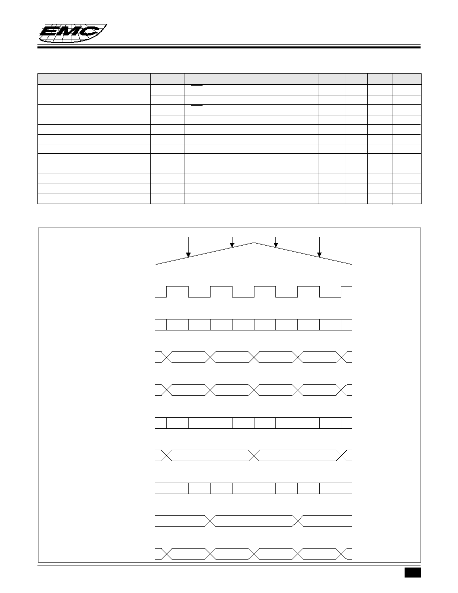
Timing
Analog input is sampled with the falling edge of CLK and output as digital data with a delay of 2.5 clocks and

5
* This specification are subject to be changed without notice.
EM19100
8-BIT 20 MSPS VIDEO A/D CONVERTER (CMOS)
1.26.1996
with the following rising edge. The delay from the clock rising edge to the data output is about 18ns.
OE pin
By connecting OE to GND output mode is obtained. By connecting to V
DD
high impedance is obtained.
About latch up
It is necessary that AV
DD
and DV
DD
pins be the common source of power supply. This is to avoid latch up
due to the voltage difference between AV
DD
and DV
DD
pins when power is ON.