
1
* This specification are subject to be changed without notice.
EM32117
16 DIGIT LCD DRIVER WITH CHECK TIME FUNCTION
3.17.1999
Preliminary
SEG25
SEG24
SEG23
SEG22
SEG21
SEG20
SEG19
SEG18
SEG17
SEG16
SEG15
SEG14
SEG13
SEG12
SEG11
SEG10
65
66
67
68
69
70
71
72
73
74
75
76
77
78
79
80
64
63
62
61
60
59
58
57
56
55
54
53
52
51
50
49
48
47
46
45
44
43
42
41
NC
NC
NC
NC
NC
NC
NC
SEG9
SEG8
SEG7
SEG6
SEG5
SEG4
SEG3
SEG2
SEG1
SEG0
GF
TEST
NC
NC
NC
NC
NC
EM32117Q
40
39
38
37
36
35
34
33
32
31
30
29
28
27
26
25
1
2
3
4
5
6
7
8
9
10
11
12
13
14
15
16
17
18
19
20
21
22
23
24
XOUT
XIN
V
SS
VC2
VC1
V3
V2
V
DD
HKS
SD1
MS2
MS1
SPARE1
SPARE2
NC
NC
NC
NC
NC
NC
NC
NC
SEG26
SEG27
SEG28
SEG29
SEG30
SEG31
COM0
COM1
COM2
COM3
ENCLND*
ENRTC*
24/12*
NC
NC
NC
NC
NC
GENERAL DESCRIPTION
EM32117 is a CMOS 16-digit LCD panel driver. The EM32117 can receive dialing information such as dialing
digits, Pause, Flash, Pulse to Tone mode from EMC EM91465 series dialer IC and display the corresponding
pattern on the LCD panel. The EM32117 also supports various indicators such as the icons of STORE, SAVE,
Speaker phone (or Hand-Free), Lower or Upper page, Hold, etc. to support high-end feature phone applications.
The EM32117 can operate in stand-alone mode to display calendar and real time clock, conversation time
(stopwatch). The EM32117 also provides check the last conversation time function.
FEATURES
� ON-HOOK check last conversation time function.
� General flag display function for LOGO indication.
� Low power consumption: 1.5
�
A (max.)
� Uses single clock 32768 Hz crystal (with built-in capacitor, no need extra capacitor).
� LCD blank 2 sec after OFF-HOOK, to protect the STW data.
� Built-in serial data interface (compatiable with EM91465 series).
� Driver for 4.5-volt, 16-digit, 1/4 duty , 1/3 bias LCD panel with built-in voltage tripler circuit.
� Display dialing phone number.
� Display calendar and real time clock (RTC) in 12 hour or 24 hour format.
� Stopwatch function for counting conversation time up to 59 minutes 59 seconds.
� Operating voltage: 1.5 VDC ( typical )
� Dice form, QFP 80 pin package, and LCM (Liquid Crystal display Module) are available.
APPLICATION
� LCD Feature phone and Digital display system.
PIN ASSIGMENT
2
Preliminary
EM32117
16 DIGIT LCD DRIVER WITH CHECK TIME FUNCTION
* This specification are subject to be changed without notice.
3.17.1999
Pin Name
Description
SPARE1, SPARE2
Need to be connected to V
SS
.
COM0~COM3
LCD panel driver common output pins.
SEG0~SEG31
LCD panel driver segment output pins.
TEST
Reserved for testing, should be left open.
MS1
Manual setting and check last conversation time input pin 1, with built-in pull-up optimal
resistor. The optimal resistor before keying=100k
, after keying change to 1M
for
reducing power consumption.
MS2
Manual setting input pin 2 with built-in pull-up; optimal resistor. The
optimal resistor before keying=100k
, after keying change to 1M
for reducing power
consumption.
SDI
Serial data input pin with built-in 150 K
pull-up resistor.
HKS
Hook switch status input pin with built-in 1 M
pull-up resistor.
V
DD
,
V
SS
Positive power supply pin.
V2, V3
Voltage tripler circuit for LCD driver.
VC1, VC2
Voltage tripler circuit for LCD driver.
XIN, XOUT
Crystal input and output pins for connecting a 32768Hz crystal (Internal built-in 2-p
capacitor).
24/12
RTC display 24 or 12 hours format selection pin (when this pin is pulled "high, RTC will
be displayed in 24 hour format. Otherwise will be display in 12 hour format).
ENCLND
Calendar enable pin. When disabled (ENCLND* = high), the Calendar field of LCD
panel will be blanked. When 12 digit LCD panels are used, Calendar should be disable
to suppress output of calendar.
ENRTC
RTC enable pin. When disabled (ENRTC* = high), the LCD panel will be blanked when
HKS pin is at high level.
GF
General Flag input pin without built-in resistor. When GF pull "High" LCD panel will
display Icon. GF pull "Low", "GF" Icon will blank.
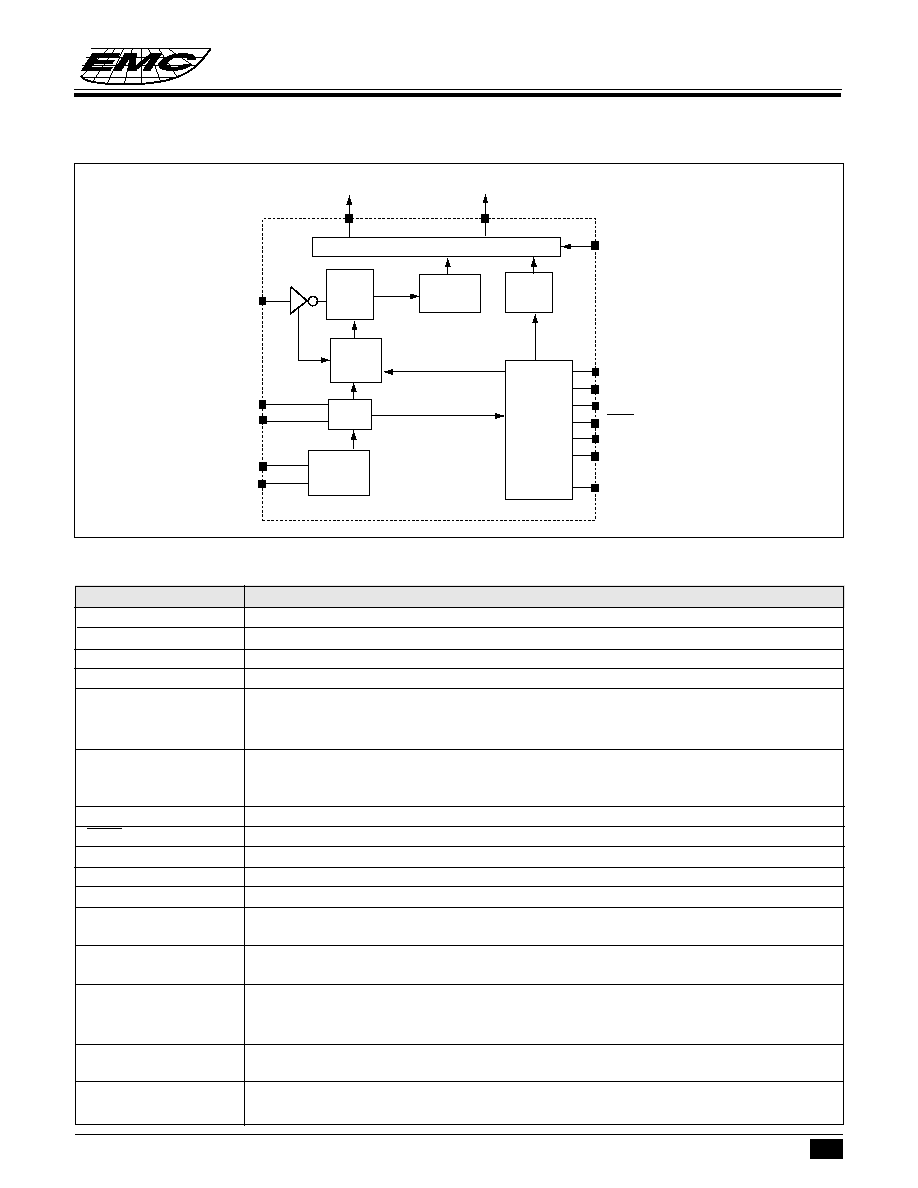
FUNCTION BLOCK DIAGRAM
PIN DESCRIPTION
SEG0~31
COM0~3
1/4 Duty 1/3 bias LCD Driver
Serial Data
Sampling
&
Decoding
Serial Data
Display Buffer
RTC/STW
Counter
GF
Timing
&
Control
Circuit
ENCLND
ENRTC
24/12
HKS
MS2
MS1
TEST
Sampling
Signal
Generator
OSC
Power
Supply
Circuit
XIN
XOUT
VDD
VSS
SD1

3
* This specification are subject to be changed without notice.
EM32117
16 DIGIT LCD DRIVER WITH CHECK TIME FUNCTION
3.17.1999
Preliminary
SEG31
SEG30
SEG29
SEG28
SEG27
SEG26
SEG25
SEG24
COM3
16f
16a
15f
15a
14f
14a
13f
13a
COM2
16g
16b
15g
15b
14g
14b
13g
13b
COM1
16e
16c
15e
15c
14e
14c
13e
13c
COM0
16d
15d
14d
13d
SEG23
SEG22
SEG21
SEG20
SEG19
SEG18
SEG17
SEG16
COM3
12f
12a
11f
11a
10f
10a
9f
9a
COM2
12g
12b
11g
11b
10g
1b
9g
9b
COM1
12e
12c
11e
11c
10e
10c
9e
9c
COM0
12d
RD
11d
Speaker
10d
HOLD
9d
Memory
SEG15
SEG14
SEG13
SEG12
SEG11
SEG10
SEG9
SEG8
COM3
8f
8a
7f
7a
6f
6a
5f
5a
COM2
8g
8b
7g
7b
6g
6b
5g
5b
COM1
8e
8c
7e
7c
6e
6c
5e
5c
COM0
8d
GF
7d
ALARM
6d
STORE
5d
PAGE
SEG7
SEG6
SEG5
SEG4
SEG3
SEG2
SEG1
SEG0
COM3
4f
4a
3f
3a
2f
2a
1f
1a
COM2
4g
4b
3g
3b
2g
2b
1g
1b
COM1
4e
4c
3e
3c
2e
2c
1e
1c
COM0
4d
AUTO
3d
LOCK
2d
SAVE
1d
MUTE
LCD Panel Description
The display font of the EM32117 LCD driver is shown as the following:
2
3
4
5
6
7
8
9
10
11
12
13
14
15
16
1
Digit #
PAUSE TONE
#
*
0
9
8
7
3
2
1
6
5
4
LO BATT
ALARM
PAGE
STORE
MEMORY
RD
SPEAKER
HOLD
AUTO
LOCK
SAVE
MUTE
BLANK
DASH
COM3
COM2
COM1
COM0
GF
ALARM
PAGE
STORE
MEMORY
RD
SPEAKER
HOLD
AUTO
LOCK
SAVE
MUTE

4
Preliminary
EM32117
16 DIGIT LCD DRIVER WITH CHECK TIME FUNCTION
* This specification are subject to be changed without notice.
3.17.1999
Figure 2 - Segment pin wiring diagram
Serial Data Interface
Since the serial data transmitters (e.g. EM91465 series dialers) may have different voltage level from EM32117,
therefore the following interconnecting scheme is recommended when using the EM32117 as a serial data
receiver. The SDO output from the serial data transmitters should be of NMOS open-drain structure as shown
below.
Data Format
When the EM32117 senses the falling edge of the Start bit, it will sample subsequent bits in the middle of each
bit. The received bit will then be assembled and decoded, and corresponding pattern will be displayed on LCD
panel. The serial data format is as follows:
Protocol
There are three categories of dialing data, and representation and interpretation of serial data is as the following:
(Note: Codes 0000 and 1111 will be interpreted as" " (blank pattern) and"-"patterns, respectively and they
will shift on LCD panel just as other digit codes.
VCC
EM32117
Dialer
2
1
3
SDO
SDI
5
4
6
Vss
2
1
3
5
4
6
Vss
Vss
Start Bit
Bit 0
Bit 1
Bit 2
Bit 3
Bit 4
Bit 5
Stop Bit
Data Bits
0
1
0
1
SEG30
SEG31
SEG28
SEG29
SEG26
SEG27
SEG24
SEG25
SEG22
SEG23
SEG20
SEG21
SEG18
SEG19
SEG16
SEG17
SEG14
SEG15
SEG12
SEG13
SEG10
SEG11
SEG8
SEG9
SEG6
SEG7
SEG4
SEG5
SEG2
SEG3
SEG0
SEG1
GF
ALARM
PAGE
STORE
MEMORY
RD
SPEAKER
HOLD
AUTO LOCK
SAVE
MUTE
5
* This specification are subject to be changed without notice.
EM32117
16 DIGIT LCD DRIVER WITH CHECK TIME FUNCTION
3.17.1999
Preliminary
Note:
1. Flash key will be treated as "clear LCD panel" command.
2. When lock condition establish.
3. MUTE and ALARM indicators will toggle with each received SDI code.
4. Any invalid data will be ignored by the EM32117.
� General flag display function. EM32117 provide General Flag Icon, when GF pin pull "high", then "GF" Icon
will be displayed. GF pin pull "low", the "GF" Icon will blank. The "GF" Icon can identify by user for special
distinguishment.
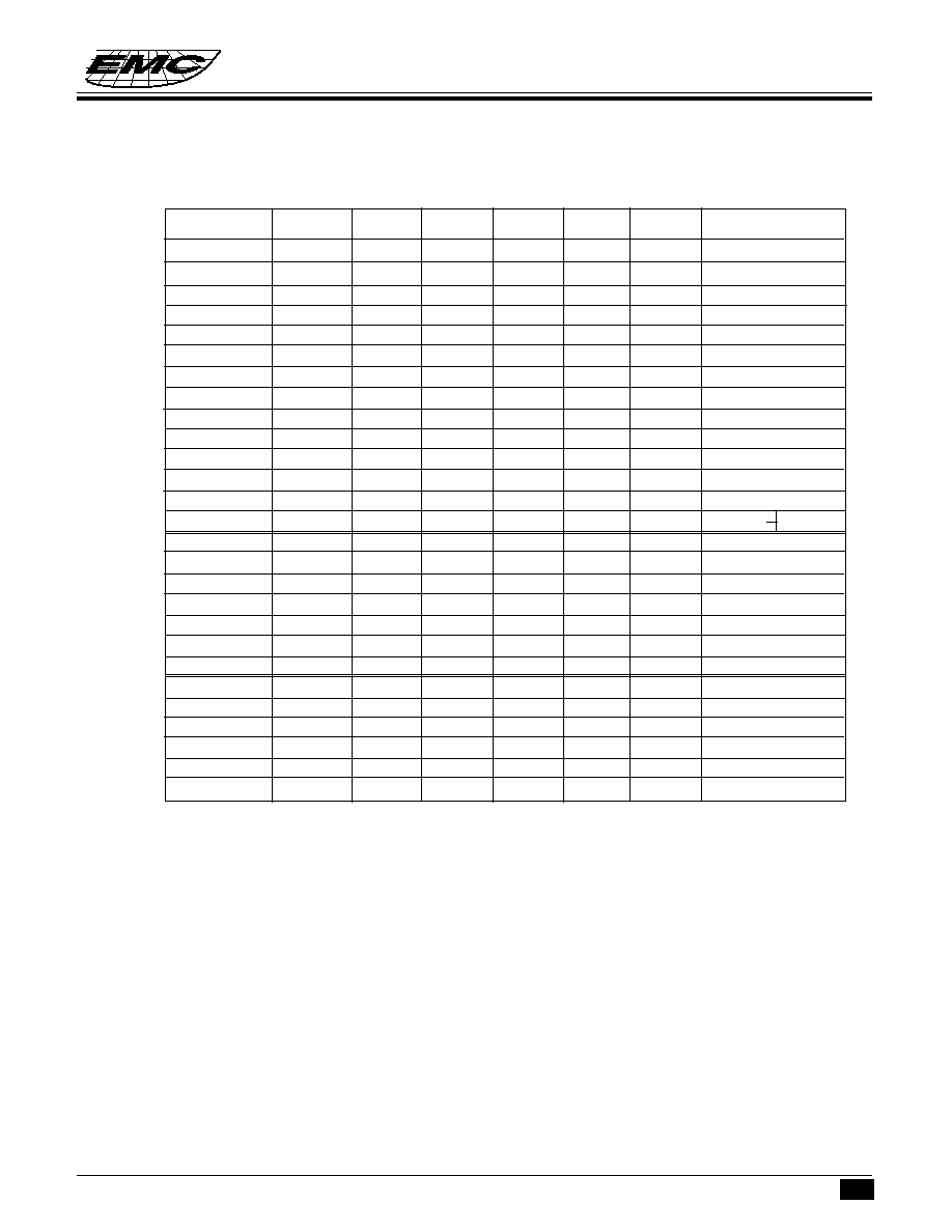
Keypad,SDO format and LCD display reference table:
Keypad
bit5
bit4
bit3
bit2
bit1
bit0
Display
1
0
0
0
0
0
1
1
2
0
0
0
0
1
0
2
3
0
0
0
0
1
1
3
4
0
0
0
1
0
0
4
5
0
0
0
1
0
1
5
6
0
0
0
1
1
0
6
7
0
0
0
1
1
1
7
8
0
0
1
0
0
0
8
9
0
0
1
0
0
1
9
0
0
0
1
0
1
0
0
"*"/T
0
0
1
0
1
1
#
0
0
1
1
0
0
P
0
0
1
1
0
1
P
*/"T"
0
0
1
1
1
0
ST
1
0
0
0
0
0
STORE
HOLD
1
0
1
0
0
0
HOLD
HF
1
0
1
0
1
0
Speaker
Page
1
0
1
1
0
0
PAGE
A
1
0
1
1
1
0
A
F
1
0
1
1
1
1
clear all display
(Lock state)
1
0
0
0
0
1
Lock
MUTE
1
0
0
0
1
0
MUTE
Note 3
1
0
0
0
1
1
ALARM
EM1~EM3
1
1
1
1
0
0
MEMORY
M1~M40
1
1
1
1
0
0
MEMORY
RD
1
1
1
1
0
1
RD
SAVE
1
1
1
1
1
0
SAVE
FUNCTION DESCRIPTION
Operation Modes and System States
Depending on which state the EM32117 is in, the system will operate in one of two modes, namely, RTC mode
and Stop-watch mode. In the State 1, as defined by the State-diagram in figure 4, the system operates in Real-
Time Clock mode, otherwise, the system operates in Stop-Watch mode. The flow chart is as follows: