
EM39LV800
8M Bits (512Kx16) Flash Memory
SPECIFICATION
This specification is subject to change without further notice. (04.09.2004 V1.0)
Page
1
of
25
General Description
The EM39LV800 is an 8M bits Flash memory organized as 512K x 16 bits. The EM39LV800
uses 2.7-3.6V power supply for Program and Erase. Featuring high performance Flash
memory technology, the EM39LV800 provides a typical Word-Program time of 14 µsec and a
typical Sector/Block-Erase time of 18 ms. The device uses Toggle Bit or Data# Polling to
detect the completion of the Program or Erase operation. To protect against inadvertent
write, the device has on-chip hardware and software data protection schemes. The device
offers typical 100,000 cycles endurance and a greater than 10 years data retention. The
EM39LV800 conforms with the JEDEC standard pin outs for x16 memories. The
EM39LV800 is offered in package types of 48-ball FBGA, 48-pin TSOP, and known good dice
(KGD). For KGD, please contact ELAN Microelectronics or its representatives for detailed
information (see Appendix at the bottom of this specification for Ordering Information).
The EM39LV800 devices are developed for applications that require memories with
convenient and economical updating of program, data or configuration, e.g., DVD player, DVD
R/W, WLAN, Router, Set-Top Box, etc.
Features
Single Power Supply
Full voltage range from 2.7 to 3.6 volts
for both read and write operations
Sector-Erase Capability
Uniform 2Kword sectors
Block-Erase Capability
Uniform
32Kword
blocks
Read Access Time
Access time: 55, 70 and 90 ns
Power Consumption
Active current: 20 mA (Typical)
Standby current: 2
µA (Typical)
Erase/Program Features
Sector-Erase Time: 18 ms (Typical)
Block-Erase Time: 18 ms (Typical)
Chip-Erase Time: 45 ms (Typical)
Word-Program
Time:
14
µs (Typical)
Chip Rewrite Time: 8 seconds (Typical)
Automatic Write Timing
Internal
V
PP
Generation
End-of-Program or End-of-Erase
Detection
Data#
Polling
Toggle
Bit
CMOS I/O Compatibility
JEDEC Standard
Pin-out and software command sets
compatible with single-power supply Flash
memory
High Reliability
Endurance cycles: 100K (Typical)
Data retention: 10 years
Package Option
48-pin
TSOP
48-pin
FBGA

EM39LV800
8M Bits (512Kx16) Flash Memory
SPECIFICATION
This specification is subject to change without further notice. (04.09.2004 V1.0)
Page
2
of
25
Functional Block Diagram
X-Decoder
Flash
Mem ory Array
Y-Decoder
I/O Buffers and Data Latches
Address Buffer &
Latches
Control Logic
Mem ory Address
CE#
OE#
W E#
DQ15-DQ0
Figure 0a: Functional Block Diagram
Pin Assignments
TSOP
Standard TSOP
1
2
3
4
5
6
7
8
9
10
11
12
13
14
15
16
17
18
19
20
21
22
23
24
25
26
27
28
29
30
31
32
33
34
35
36
37
38
39
40
41
42
43
44
45
46
47
48
A16
V
SS
DQ15
DQ7
DQ14
DQ6
DQ13
DQ5
DQ12
DQ4
V
DD
DQ11
DQ3
DQ10
DQ2
DQ9
DQ1
DQ8
DQ0
OE#
V
SS
CE#
A0
A1
A2
A3
A4
A5
A6
A7
A17
NC
NC
WE#
A8
A9
A10
A11
A12
A13
NC
NC
A14
A15
NC
A18
NC
NC
Figure 0b: TSOP Pin Assignments
EM39LV800
8M Bits (512Kx16) Flash Memory
SPECIFICATION
This specification is subject to change without further notice. (04.09.2004 V1.0)
Page
3
of
25
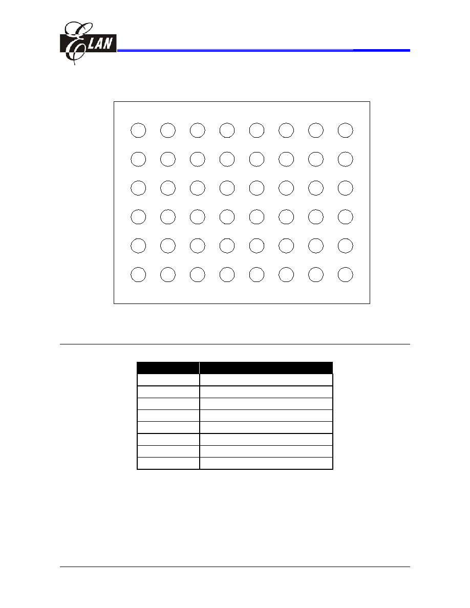
FBGA
A13
A9
W E#
A7
A3
FBGA
Top View, Balls Facing Down
A12
A14
A15
A16
DQ15
V
SS
A8
A10
A11
DQ7
DQ14
DQ13
DQ6
NC
NC
DQ5
DQ12
V
DD
DQ4
NC
A18
NC
DQ2
DQ10
DQ11
DQ3
A17
A4
A6
A2
A5
A1
DQ0
A0
DQ8
CE#
DQ9
OE#
DQ1
V
SS
NC
NC
NC
Figure 0c: FBGA Pin Assignments
Pin Description
Pin Name
Function
A0≠A18 19
addresses
DQ15≠DQ0 Data
inputs/outputs
CE# Chip
enable
OE# Output
enable
WE# Write
enable
V
DD
2.7 ~ 3.6 volt single power supply
V
SS
Device
ground
NC
Pin not connected internally
Table 1: Pin Description

EM39LV800
8M Bits (512Kx16) Flash Memory
SPECIFICATION
This specification is subject to change without further notice. (04.09.2004 V1.0)
Page
4
of
25
Device Operation
The EM39LV800 uses Commands to initiate the memory operation functions. The
Commands are written to the device by asserting WE# Low while keeping CE# Low. The
address bus is latched on the falling edge of WE# or CE#, whichever occurs last. The data
bus is latched on the rising edge of WE# or CE#, whichever occurs first.
Read
The Read operation of the EM39LV800 is controlled by CE# and OE#. Both have to be Low
for the system to obtain data from the outputs. CE# is used for device selection. When CE#
is high, the chip is deselected and only standby power is consumed. OE# is the output
control and is used to gate data from the output pins. The data bus is in high impedance state
when either CE# or OE# is high. Refer to the Read Cycle Timing Diagram in Figure 1 for
further details.
Word Program
The EM39LV800 is programmed on a word-by-word basis. Before programming, the sector
where the word is located must be erased completely. The Program operation is
accomplished in three steps:
The first step is a three-byte load sequence for Software Data Protection.
The second step is to load word address and word data. During the Word Program
operation, the addresses are latched on the falling edge of either CE# or WE#, whichever
occurs last; and the data is latched on the rising edge of either CE# or WE#, whichever
occurs first.
The third step is the internal Program operation which is initiated after the rising edge of
the fourth WE# or CE#, whichever occurs first. The Program operation, once initiated,
will be completed within 20 µs. See Figures 2 and 3 for WE# and CE# controlled
Program operation timing diagrams respectively and Figure 15 for flowchart.
During the Program operation, the only valid reads are Data# Polling and Toggle Bit. During
the internal Program operation, the host is free to perform additional tasks. Any command
issued during the internal Program operation is ignored.
EM39LV800
8M Bits (512Kx16) Flash Memory
SPECIFICATION
This specification is subject to change without further notice. (04.09.2004 V1.0)
Page
5
of
25
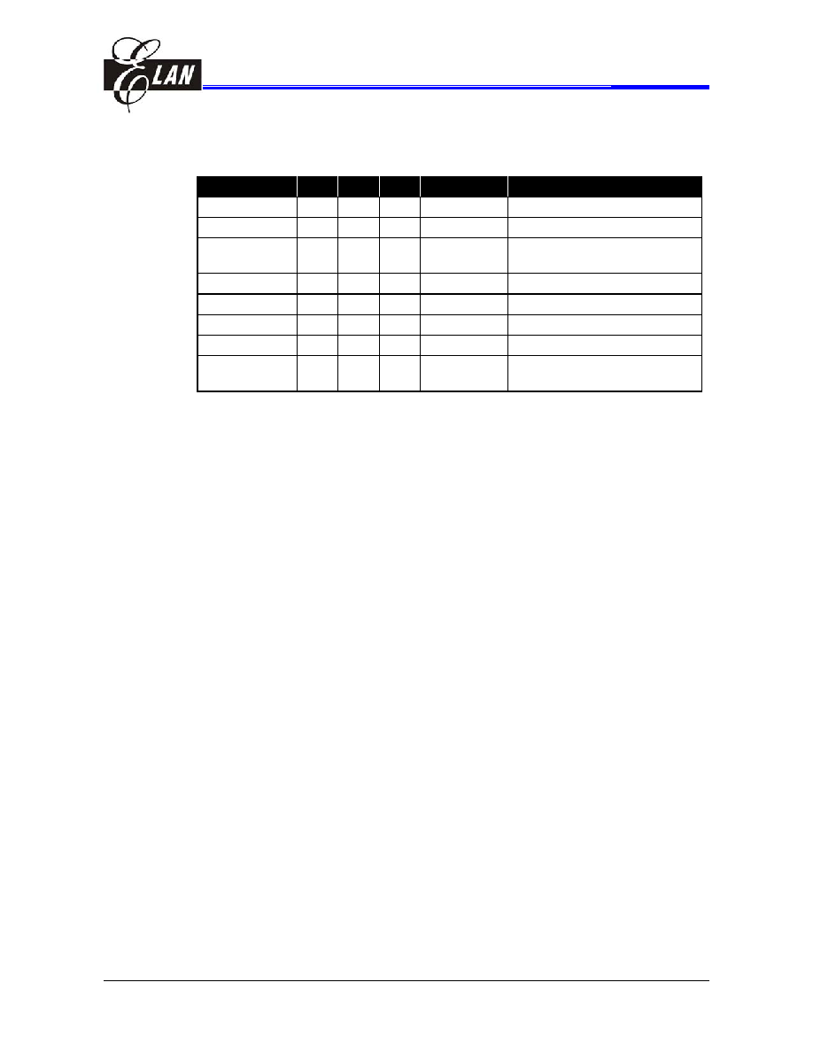
EM39LV800 Device Operation
Operation
CE# OE# WE#
DQ
Address
Read V
IL
V
IL
V
IH
D
OUT
A
IN
Program V
IL
V
IH
V
IL
D
IN
A
IN
Erase V
IL
V
IH
V
IL
X
*
Sector or Block address, XXH for
Chip-Erase
Standby V
IH
X X
High
Z X
Write Inhibit
X
V
IL
X High
Z/D
OUT
X
Write Inhibit
X
X
V
IH
High
Z/D
OUT
X
Software Mode
V
IL
V
IL
V
IH
See
Table
3
Product
Identification
*
X can be V
IL
or V
IH
, but no other value.
Table 2: EM39LV800 Device Operation
Write Command/Command Sequence
The EM39LV800 provides two software methods to detect the completion of a Program or
Erase cycle in order to optimize the system write cycle time. The software detection includes
two status bits: Data# Polling (DQ7) and Toggle Bit (DQ6). The End-of-Write detection mode
is enabled after the rising edge of WE#, which initiates the internal Program or Erase
operation. The actual completion of the write operation is asynchronous with the system;
therefore, either a Data# Polling or Toggle Bit read may be simultaneous with the completion
of the write cycle. If this occurs, the system may possibly get an erroneous result, i.e., valid
data may appear to conflict with either DQ7 or DQ6. In order to prevent such spurious
rejection, when an erroneous result occurs, the software routine should include an additional
two times loop to read the accessed location. If both reads are valid, then the device has
completed the write cycle, otherwise the rejection is valid.
Chip Erase
The EM39LV800 provides Chip-Erase feature, which allows the entire memory array to be
erased to logic "1" state. The Chip-Erase operation is initiated by executing a six-byte
command sequence with Chip-Erase command (10H) at address 5555H in the last byte
sequence. The Erase operation begins with the rising edge of the sixth WE# or CE#,
whichever occurs first. During the Erase operation, the only valid reads are Toggle Bit and
Data# Polling. See Table 3 for the command sequence, Figure 6 for timing diagram, and
Figure 17 for the flowchart. Any commands issued during the Chip-Erase operation are
ignored.