 | –≠–ª–µ–∫—Ç—Ä–æ–Ω–Ω—ã–π –∫–æ–º–ø–æ–Ω–µ–Ω—Ç: EM65H134 | –°–∫–∞—á–∞—Ç—å:  PDF PDF  ZIP ZIP |

ELAN MICROELECTRONICS CORP.
PAGE
1
,
∞
ALL RIGHTS STRICTLY RESERVED, ANY PORTION IN THIS PAPER SHALL NOT BE REPRODUCED, COPIED WITHOUT PERMISSION.
1.2 /2001/ 7/16
240 Channel Segment Driver for Dot matrix STN Liquid
Crystal Display with Low Voltage Drive
EM65H134
Contents
1. General description
2
2. Feature
2
3. Applications
2
4. Pin configurations (package)
3
5. Functional block diagram
4
6. Pin descriptions
5
7. Function description
7
8. Absolute maximum rating
16
9. DC electrical characteristics
18
10. AC electrical characteristics
20
11. Timing diagrams
21
12. Application circuit
22
ELAN MICROELECTRONICS CORP.
PAGE
2
,
∞
ALL RIGHTS STRICTLY RESERVED, ANY PORTION IN THIS PAPER SHALL NOT BE REPRODUCED, COPIED WITHOUT PERMISSION.
1.2 /2001/ 7/16
General Description
The EM65H134 is a 240-channel segment LCD driver LSI, Which drives a dot matrix STN liquid
crystal display at low power. The EM65H134 operates with a low 5V LCD drive voltage and a low 3V
logic voltage. The EM65H134 includes shadowing correction circuit in order to improve image quality.
The EM65H134 is packaged in a fine pitch slim TCP( slim type carrier package) technology, it is deal
for substantially decreasing the size of LCD module frame.
Feature
- Duty cycle: Up to 1/300
- LCD drive voltage: 3.5 to 5.5 V
- 240 LCD drive circuits
- Operating voltage: 2.7 to 5.5 V
- Eight data bits
- Shift clock speed
--
25 MHz max/3 V
--
40 MHz max/5 V
- Shadowing correction circuit
- Display-off function
- Slim-TCP
--
Output lead pitch: 70
m
--
User area: 5.5mm
- Automatic generation of the chip enable signal
- Standby function
Applications
- PDA
- Dictionary
- Message display product
ELAN MICROELECTRONICS CORP.
PAGE
3
,
∞
ALL RIGHTS STRICTLY RESERVED, ANY PORTION IN THIS PAPER SHALL NOT BE REPRODUCED, COPIED WITHOUT PERMISSION.
1.2 /2001/ 7/16
Pin Configuration
S
1
S
2
.
.
.
.
.
.
.
.
.
.
.
.
.
.
.
.
.
.
.
.
.
.
.
.
.
.
.
.
S
2
3
9
S
2
4
0
E M 6 5 H 1 3 4
T o p V i e w
267--------------------------------------------------------------------------------------------241
1----------------------------------------------------------------------------------------------------------------------240
D
I
R
E
I
O
1
/
D
S
P
O
F
D
I
0
D
I
1
D
I
2
D
I
3
D
I
4
D
I
5
D
I
6
D
I
7
X
C
K
L
P
F
R
E
I
O
2
C
C
1
C
C
2
C
C
3
C
C
4
V
S
S
V
1
R
V
0
R
V
M
R
V
M
L
V
0
L
V
1
L
V
D
D
Note: The pin configuration is LSI chip, not TCP.
Figure1. Pin configuration
ELAN MICROELECTRONICS CORP.
PAGE
4
,
∞
ALL RIGHTS STRICTLY RESERVED, ANY PORTION IN THIS PAPER SHALL NOT BE REPRODUCED, COPIED WITHOUT PERMISSION.
1.2 /2001/ 7/16
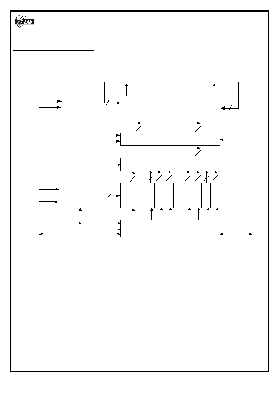
Functional Block Diagram
240 bits 3-level driver
(Liquid crystal display driver circuit)
Correction circuit
Line latch circuit
Shift register
data
latch
....
F R
/ D S P O F
3
3
8
8
8
8
8
8
8
240
240
Data shift and
arithmetic circuit
LP
X C K
DIR
E I O 2
E I O 1
V
0R
V
0L
240
239
2
1
,
........,
..........
..........
,.........
,
S
S
S
S
8
240
DI0~DI7
CC1~CC4
DD
V
SS
V
V
1R
,
V
M R
,
V
1L
,
V
M L
,
8
Figure 2. Block diagram

ELAN MICROELECTRONICS CORP.
PAGE
5
,
∞
ALL RIGHTS STRICTLY RESERVED, ANY PORTION IN THIS PAPER SHALL NOT BE REPRODUCED, COPIED WITHOUT PERMISSION.
1.2 /2001/ 7/16
Pin Descriptions
Table1 pin description
Symbol
Pin No. I/O Connected to
Functions
V
DD
264
I
Power Supply Power supply for internal logic connects to
+2.7 to +5.5V
V
SS
244
I
GND
Connect to Ground
V
0R
, V
0L
V
MR
, V
ML
V
1R
, V
1L
266,242
267,241
256,243
I
Power Supply Power supply for LCD driver level
Ensure that the voltage are set such that
V
1
<V
M
<V
0
, V
M
=0.5(V
0
-V
1
)
DI
0
≠ DI
7
260 t0
253
I
Controller
Input for display data
input data into 8 pins DI
0
≠ DI
7
XCK
252
I
Controller
Clock signal for taking display data
Data is read on the falling of the clock
pulse
LP
251
I
Controller
Latch signal for display data
Data is latched on the falling edge of the
clock pulse
FR
250
I
Controller
AC signal for LCD driver
Input a frame inversion signal
DIR
263
I
Controller
Directional selection for reading display
data
DIR
Data read direction
H
S
240
to S
1
L
S
1
to S
240
/DSPOF
261
I
Controller
When the signal is low
the output (S
1
≠
S
240
) of LCD drive be set to level V
M
EIO
1
EIO
2
262,249 I/O
Controller
Input/output for chip selection
In output state
the output pin must
connect to input pin of next EM65H134
In input state
the input pin of the fist
EM65H134 must connect to Vss
the other
input pin must connect to the output pin of
previous EM65H134.
DIR
EIO
1
EIO
2
H
output
input
L
input
output