
1
* This specification are subject to be changed without notice.
10.8.2001
EM73361A
EM73361A
EM73361A
EM73361A
EM73361A
4-BIT MICRO-CONTROLLER FOR LCD PRODUCT
4-BIT MICRO-CONTROLLER FOR LCD PRODUCT
4-BIT MICRO-CONTROLLER FOR LCD PRODUCT
4-BIT MICRO-CONTROLLER FOR LCD PRODUCT
4-BIT MICRO-CONTROLLER FOR LCD PRODUCT
GENERAL DESCRIPTION
GENERAL DESCRIPTION
GENERAL DESCRIPTION
GENERAL DESCRIPTION
GENERAL DESCRIPTION
EM73361A is an advanced single chip CMOS 4-bit micro-controller. It contains 3K-byte ROM, 52-nibble RAM,
4-bit ALU, 13-level subroutine nesting, 22-stage time base, two 12-bit timer/counters for the kernel function.
EM73361A also contains 3 interrupt sources, 1 input port, 4 bidirection I/O ports, built-in watch-dog-timer
counter, tone generator and LCD driver (27x3 to 13x3).
Except low-power consumption and high speed, EM73361A also have a sleep mode operation for power saving.
FEATURES
FEATURES
FEATURES
FEATURES
FEATURES
∑ Operation voltage
: 2.2V to 3.6V(clock frequency : 32K Hz).
∑ Clock source
: Single clock system for crystal, connect a external resistor or external clock
source available by mask option.
∑ Instruction set
: 109 powerful instructions.
∑ Instruction cycle time
: 122µs for 32K Hz.
∑ ROM capacity
: 3072 X 8 bits.
∑ RAM capacity
: 52 X 4 bits.
∑ Input port
: 1 port (P0)(Pull-up and pull-down resistor with wakeup function available by
mask option).
∑ Bidirection port
: 4 ports (P4, P5, P6, P7) are available by mask option. (each I/O pin is push-pull
and open-drain available by mask option) P4.0 is high current pin (P4.0 and
TONE available by mask option). P4.2~P4.3, P5, P6 and P7 are shared with
SEG26-SEG13 by mask option.
∑ 12-bit timer/counter
: Two 12-bit timer/counters are programmable for timer mode.
∑ Low voltage reset (LVR) : Reset at 1.5V, and reset release at 1.8V.
∑ Tone generator
: There is a built-in tone generator.
∑ Built-in time base counter : 22 stages.
∑ Subroutine nesting
: Up to 13 levels.
∑ Interrupt
: External . . . . . 2 External interrupt (INT0, INT1).
Internal . . . . . . 2 Timer overflow interrupts.
1 Time base interrupt.
∑ LCD driver
: 27 X 3 to 13 X 3 dots available by mask option. Capacitor divider and resistor
divider are available by mask option.1/3, 1/2 and static three kinds of duty (1/2
bias) selectable. The programming method of LCD driver is I/O mapping.
∑ Built-in watch-dog-timer : The WDT is enabled or disabled by mask option.
∑ Power saving function
: Sleep mode and Hold mode.
∑ Package type
: EM73361AAH
Chip form
46 pins.
EM73361AAQ
QFP 100 pins.
APPLICATIONS
APPLICATIONS
APPLICATIONS
APPLICATIONS
APPLICATIONS
EM73361A is suitable for application in family appliance, consumer products, hand held games and the toy
controller.

2
* This specification are subject to be changed without notice.
10.8.2001
EM73361A
EM73361A
EM73361A
EM73361A
EM73361A
4-BIT MICRO-CONTROLLER FOR LCD PRODUCT
4-BIT MICRO-CONTROLLER FOR LCD PRODUCT
4-BIT MICRO-CONTROLLER FOR LCD PRODUCT
4-BIT MICRO-CONTROLLER FOR LCD PRODUCT
4-BIT MICRO-CONTROLLER FOR LCD PRODUCT
PIN CONFIGURATIONS
PIN CONFIGURATIONS
PIN CONFIGURATIONS
PIN CONFIGURATIONS
PIN CONFIGURATIONS
1
2
3
4
5
6
7
8
9
10
11
12
13
14
15
16
17
18
19
20
21
22
23
24
25
26
27
28
29
30
50
49
48
47
46
45
44
43
42
41
40
39
38
37
36
35
34
33
32
31
80
79
78
77
76
75
74
73
72
71
70
69
68
67
66
65
64
63
62
61
60
59
58
57
56
55
54
53
52
51
81
82
83
84
85
86
87
88
89
90
91
92
93
94
95
96
97
98
99
100
NC
NC
NC
NC
P7.1/SEG15
P7.2/SEG14
P7.3/SEG13
SEG12
SEG11
SEG10
SEG9
SEG8
SEG7
SEG6
SEG5
SEG4
SEG3
NC
NC
NC
NC
NC
NC
NC
NC
NC
NC
NC
SEG2
SEG1
SEG0
COM1
COM0
VEE
VB
VA
XIN
XOUT
NC
NC
NC
NC
NC
NC
NC
NC
NC
NC
NC
NC
NC
NC
P4.1/WDT
P4.0/TONE
TONE
P0.3/WAKEUP3
P0.2(INT0)/WAKEUP2
P0.1/WAKEUP1
P0.0(INT1)/WAKEUP0
RESET
NC
NC
NC
NC
NC
NC
NC
NC
NC
NC
TEST
NC
NC
NC
NC
NC
NC
NC
NC
NC
NC
EM73361AAQ
QFP 100
NC
NC
NC
NC
VDD
VSS
P4.3/SEG25
P4.2/SEG26
COM2
P5.0/SEG24
P5.2/SEG22
P5.1/SEG23
P6.0/SEG20
P5.3/SEG21
P6.2/SEG18
P6.1/SEG19
P7.0/SEG16
P6.3/SEG17
NC

3
* This specification are subject to be changed without notice.
10.8.2001
EM73361A
EM73361A
EM73361A
EM73361A
EM73361A
4-BIT MICRO-CONTROLLER FOR LCD PRODUCT
4-BIT MICRO-CONTROLLER FOR LCD PRODUCT
4-BIT MICRO-CONTROLLER FOR LCD PRODUCT
4-BIT MICRO-CONTROLLER FOR LCD PRODUCT
4-BIT MICRO-CONTROLLER FOR LCD PRODUCT
Symbol
Symbol
Symbol
Symbol
Symbol
Pin-type
Pin-type
Pin-type
Pin-type
Pin-type
Function
Function
Function
Function
Function
V
D D
Power supply (+)
V
SS
Power supply (-)
RESET
RESET-A
System reset input signal, low active
mask option :
none
pull-up
XIN
OSC-A/OSC-F
Crystal/external resistor or external clock source connecting pin
XOUT
OSC-A/OSC-F
Crystal/external resistor connecting pin
P0.0(INT1)/WAKEUP0,
INPUT-J
2-bit input port with external interrupt sources input and Sleep/Hold
P0.2(INT0)/WAKEUP2
releasing function
mask option :
wakeup enable, pull-up
wakeup enable, none
wakeup disable, pull-up
wakeup disable, none
wakeup disable, pull-down
P0.1/WAKEUP1,
INPUT-H
2-bit input port with Sleep/Hold releasing function
P0.3/WAKEUP3
mask option :
wakeup enable, pull-up
wakeup enable, none
PIN DESCRIPTIONS
PIN DESCRIPTIONS
PIN DESCRIPTIONS
PIN DESCRIPTIONS
PIN DESCRIPTIONS
FUNCTION BLOCK DIAGRAM
FUNCTION BLOCK DIAGRAM
FUNCTION BLOCK DIAGRAM
FUNCTION BLOCK DIAGRAM
FUNCTION BLOCK DIAGRAM
Interrupt
Control
Time
Base
12-bit
timer
counter
(TA,TB)
System Control
Instruction Decoder
Instruction Register
ROM
PC
Data Bus
Reset
Control
Frequency
doubler
Timing
Generator
Sleep Mode
Control
Data pointer
ACC
ALU
Flag
Z
C
S
G
Stack pointer
Stack
RAM
HR
LR
I/O Control
P0.0(INT1)/WAKEUP0
P0.1/WAKEUP1
P0.2(INT0)/WAKEUP2
P0.3/WAKEUP3
RESET
Clock
Generator
XIN
XOUT
LCD
driver
Tone generator
WDT
VA
VB
VEE
COM0~COM2
SEG0~SEG12
P4.0/TONE
P4.1/WDT
TONE
P4,P5,P6,P7/SEG(26..13)

4
* This specification are subject to be changed without notice.
10.8.2001
EM73361A
EM73361A
EM73361A
EM73361A
EM73361A
4-BIT MICRO-CONTROLLER FOR LCD PRODUCT
4-BIT MICRO-CONTROLLER FOR LCD PRODUCT
4-BIT MICRO-CONTROLLER FOR LCD PRODUCT
4-BIT MICRO-CONTROLLER FOR LCD PRODUCT
4-BIT MICRO-CONTROLLER FOR LCD PRODUCT
FUNCTION DESCRIPTIONS
FUNCTION DESCRIPTIONS
FUNCTION DESCRIPTIONS
FUNCTION DESCRIPTIONS
FUNCTION DESCRIPTIONS
PROGRAM ROM ( 3K X 8 bits )
PROGRAM ROM ( 3K X 8 bits )
PROGRAM ROM ( 3K X 8 bits )
PROGRAM ROM ( 3K X 8 bits )
PROGRAM ROM ( 3K X 8 bits )
3 K x 8 bits program ROM contains user's program and some fixed data .
The basic structure of program ROM can be divided into 4 parts.
1. Address 000h: Reset start address.
2. Address 002h - 00Ch: 4 kinds of interrupt service routine entry addresses .
3. Address 00Eh-086h : SCALL subroutine entry address, only available at 00Eh,016h,01Eh,026h, 02Eh,
036h, 03Eh, 046h, 04Eh, 056h, 05Eh, 066h, 06Eh, 076h ,07Eh, 086h .
4. Address 000h - 7FFh : LCALL subroutine entry address
5. Address 000h - BFFh : Except used as above function, the other region can be used as user's program region.
address 3072 x 8 bits
000h
Reset start address
002h
INT0 ; External interrupt service toutine entry address
004h
006h
TRGA; Timer/counter A interrupt service routine entry address
008h
TRGB; Timer/counter B interrupt service routine entry address
00Ah
TBI; Time base interrupt service routine entry address
00Ch
INT1; External interrupt service routine entry address
00Eh
086h
BFFh
Symbol
Symbol
Symbol
Symbol
Symbol
Pin-type
Pin-type
Pin-type
Pin-type
Pin-type
Function
Function
Function
Function
Function
wakeup disable, pull-up
wakeup disable, pull-down
wakeup disable, none
P4.0/TONE
I/O-O
1-bit bidirection I/O pin or inverse tone generator output
mask option :
TONE enable, push-pull, high current PMOS
TONE disable, open-drain
TONE disable, push-pull, high current PMOS
TONE disable, push-pull, low current PMOS
P4.1/WDT
I/O-D
1-bit bidirection I/O pin with watch-dog-timer output
mask option :
open-drain
push-pull
P4(2..3)/SEG(26..25)
I/O-P
4-bit bidirection I/O ports are shared with LCD segment pins
P5(0..3)/SEG(24..21)
mask option :
segment enable, open-drain
P6(0..3)/SEG(20..17)
segment disable, push-pull
P7(0..3)/SEG(16..13)
segment disable, open-drain
TONE
Built-in tone generator output
VA, VB, VEE
Connect the capacitors for LCD bias voltage
COM0~COM2
LCD common output pins
SEG0~SEG12
LCD segment output pins
TEST
Tie Vss as package type, no connecting as COB type
SCALL, subroutine call entry address
.
.
.
5
* This specification are subject to be changed without notice.
10.8.2001
EM73361A
EM73361A
EM73361A
EM73361A
EM73361A
4-BIT MICRO-CONTROLLER FOR LCD PRODUCT
4-BIT MICRO-CONTROLLER FOR LCD PRODUCT
4-BIT MICRO-CONTROLLER FOR LCD PRODUCT
4-BIT MICRO-CONTROLLER FOR LCD PRODUCT
4-BIT MICRO-CONTROLLER FOR LCD PRODUCT
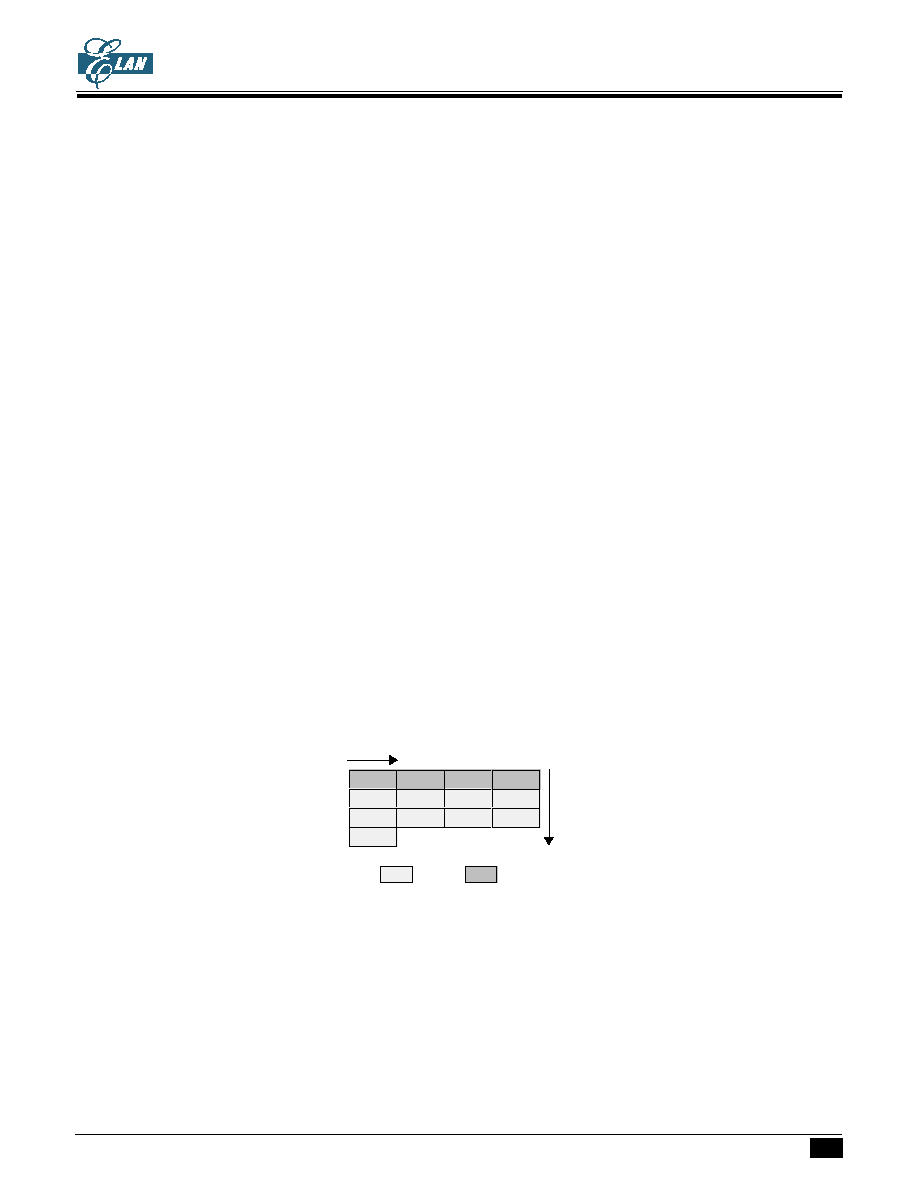
STACK:
There are 13 - level (maximum) stack for user using for subroutine (including interrupt and CALL). User
can assign any level be the starting stack by giving the level number to stack pointer (SP).
ZERO- PAGE:
From 00h to 0Fh is the location of zero-page. It is used as the pointer in zero -page addressing mode for the
instruction of "STD #k,y; ADD #k,y; CLR y,b; CMP k,y".
PROGRAM EXAMPLE: To wirte immediate data "07h" to address "03h" of RAM and to clear bit 2 of RAM.
STD #07h, 03h ; RAM[03]
07h
CLR 0Eh,2 ; RAM[0Eh]
2
0
Increment
Address
20h - 2Fh
30h - 33h
Level 0
Level 4
Level 8
Level 12
Level 1
Level 5
Level 9
Level 2
Level 6
Level 10
Level 3
Level 7
Level 11
Increment
00h - 0Fh
10h - 1Fh
Stack
Zero-page
DATA RAM ( 52-nibble )
DATA RAM ( 52-nibble )
DATA RAM ( 52-nibble )
DATA RAM ( 52-nibble )
DATA RAM ( 52-nibble )
There is total 52 - nibble data RAM from address 00 to 33h
Data RAM includes 3 parts: zero page region, stacks and data area.
LDAX
LDAX
LDAX
LDAX
LDAX
Acc
Acc
Acc
Acc
Acc
ROM[DP]
ROM[DP]
ROM[DP]
ROM[DP]
ROM[DP]
L
L
L
L
L
LDAXI
LDAXI
LDAXI
LDAXI
LDAXI
Acc
Acc
Acc
Acc
Acc
ROM[DP]
ROM[DP]
ROM[DP]
ROM[DP]
ROM[DP]
H
H
H
H
H
,DP+1
,DP+1
,DP+1
,DP+1
,DP+1
DP is a 12-bit data register which can store the program ROM address to be the pointer for the ROM code data.
First, user load ROM address into DP by instruction "STADPL, STADPM, STADPH", then user can get the
lower nibble of ROM code data by instruction "LDAX" and higher nibble by instruction "LDAXI".
PROGRAM EXAMPLE: Read out the ROM code of address 777h by table-look-up instruction.
LDIA #07h;
STADPL ; [DP]
L
07h
STADPM ; [DP]
M
07h
STADPH
; [DP]
H
07h, Load DP=777h
:
LDL #00h;
LDH #03h;
LDAX
; ACC
6h
STAMI
; RAM[30]
6h
LDAXI
; ACC
5h
STAM
; RAM[31]
5h
;
ORG 777h
DATA 56h;
:
Table-look-up instruction is depended on the Data Pointer ( DP ) to indicate to ROM address, then to get the
ROM code data.
User's program and fixed data are stored in the program ROM. User's program is according the PC value
to send next executed instruction code. Fixed data can be read out by table-look-up instruction.