
ELAN MICROELECTRONICS CORP.
No. 12, Innovation 1
st
RD., Science-Based Industrial Park
Hsin Chu City, Taiwan.
TEL: (03) 5639977
FAX: (03) 5630118
EM785830AD
8-BIT MICRO-CONTROLLER
Version 1.5
Version History
Specification Revision History
Version Content
eFH5830AD
1.0 Initial
version
1.1
Add 17.91MHz main CLK
1.2
ADD eFHP5830D, eFHP5830AD, and eFHP5830BD package
1.3
ADD the description about ADC's offset voltage
1.4
Modify stack level from 16 to 12
Modify program ROM size from 4K to 16K
Rename "eFH5830D" to eFH5830AD
Remove IDLE mode
Remove 17.9MHz main CLK
1.5
Rename from eFH5830AD to EM785830AD
Relative to EM785830AD's ROM-less, OTP and mask:
ROM-less OTP
Mask
EM78P5830D
ICE5830
EM78P5830AD
EM785830AD
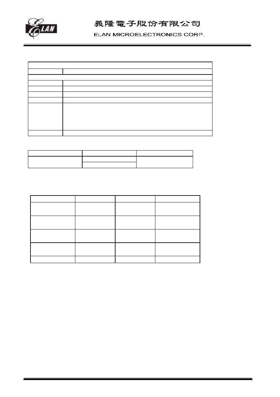
Difference between EM785830AD/EM78P5830D/EM78P5830AD
Some differences are betweenEM785830AD, EM78P5830D and EM78P5830AD, these differences are list at next
table:
EM78P5830D
EM78P5830AD
EM785830AD
ADIS
(code option bit9)
Un-effect Un-effect Must
=
1
VERSEL
(code option bit10)
Un-effect
Must = 0
Must = 0
PHO
(code option bit11)
Un-effect
Must = 0
Must = 0
MS
(
IOCC page1
bit0)
Must = 1
Un-effect
Un-effect
Stack number
16 16 12

EM785830AD
8-bit Micro-controller
__________________________________________________________________________________________________________________________________________________________________
* This specification is subject to be changed without notice.
1
12/14/2004 (V1.4)
User Application Note
(Before using this chip, take a look at the following description note, it includes important messages.)
1. There are some undefined bits in the registers. The values in these bits are unpredicted. These
bits are not allowed to use. We use the symbol "-" in the spec to recognize them. A fixed value
must be write in some specific unused bits by software or some unpredicted wrong will occur
These bits are as below:
Register
Register
PAGE
Bit
Default value Initial Setting value
(by user software)
Effect
R7
1
1
0
0
RAM access will error
RA 2 7 X
1
Un-expect
error
RD
0
5~6
X
0
Power consumption increase
RE 0 1~3 0
0
Un-expect
error
IOC6 1 7
0
0
LCD
display
error
IOC8
0
1~7
1
0
Power consumption increase
IOC8
1
1~7
0
0
Power consumption increase
IOCA
1
3,6
X
0
Power consumption increase
IOCB
0
0~7
1
0
Power consumption increase
IOCC
0
4~7
1
0
Power consumption increase
IOCC 1 0
X
1
AD function will error
IOCC 1 3~7 X
0
Un-expect error
IOCE 0 0~3 0
0
Un-expect
error
IOCF 0 6~7 0
0
Un-expect
error
2. You will see some names for the register bits definitions. Some name will be appear very
frequently in the whole spec. The following describes the meaning for the register's definitions
such as bit type, bit name, bit number and so on.
7
6
5
4
3
2
1
0
RAB7
RAB6
BAB5
RAB4
RAB2
RAB0
R/W -0
R/W -0
R-1
R/W -1
R
R/W
Bit type
Bit name
Bit number
read/write
(default value=0)
read/write
(default value=1)
read only
(w/o default value)
read/write
(w/o default value)
PAGE0
RA
Register name and its page
-
RAB1
(undefined) not allowed to use
R-0
read only
(default value=0)
read only
(default value=1)
3. Always set IOCC PAGE1 bit 0 = 1 otherwise partial ADC function cannot be used.
4. Please do not switch MCU operation mode from normal mode to sleep mode directly. Before into
sleep mode, please switch MCU to green mode.
5. While switching main clock (regardless of high freq to low freq or on the other hand), adding 6
instructions delay (NOP) is required.
6.
Offset voltage will effect ADC
'
s result, please refer to figure 20 to detail.

EM785830AD
8-bit Micro-controller
__________________________________________________________________________________________________________________________________________________________________
* This specification is subject to be changed without notice.
2
12/14/2004 (V1.4)
I. General Description
The EM785830AD is an 8-bit RISC type microprocessor with low power, high speed CMOS technology. There
are 16Kx13 bits Memory within it. This integrated single chip has an on_chip watchdog timer (WDT), program ROM,
data RAM, LCD driver, programmable real time clock/counter, internal interrupt, power down mode, built-in three-wire
SPI, dual PWM(Pulse Width Modulation), 6-channel 10-bit A/D converter and tri-state I/O.
II. Feature
CPU
�
Operating voltage : 2.2V~5.5V at main CLK less then 3.58MHz.
Main CLK(Hz)
Under 3.58M
7.16M
10.74M
14.3M
Operating Voltage(min)
2.2
2.5
3
3.6
�
16k x 13 on chip Program Memory.
�
0.5k x 8 on chip data RAM
�
Up to 31 bi-directional tri-state I/O ports
�
12 level stack for subroutine nesting
�
8-bit real time clock/counter (TCC)
�
two 8-bit counters : COUNTER1 and COUNTER2
�
On-chip watchdog timer (WDT)
�
99.9 single instruction cycle commands
�
Three operating modes (Main clock can be programmed from 447.829k to 14.3MHz generated by internal
PLL)
Mode
CPU status
Main clock
32.768kHz clock status
Sleep mode
Turn off
Turn off
Turn off
Green mode
Turn on
Turn off
Turn on
Normal mode
Turn on
Turn on
Turn on
�
Input port interrupt function
�
12 interrupt source, 4 external, 8 internal
�
Dual clocks operation (Internal PLL main clock , External 32.768KHz)
SPI
�
Serial Peripheral Interface (SPI) : a kind of serial I/O interface
�
Interrupt flag available for the read buffer full or transmitter buffer empty.
�
Programmable baud rates of communication
�
Three-wire synchronous communication. (shared with IO)
PWM
�
Dual PWM (Pulse Width Modulation) with 10-bit resolution
�
Programmable period (or baud rate)
�
Programmable duty cycle
ADC
�
Operating : 2.5V5.5V
�
6-channel 10-bit successive approximation A/D converter
�
Internal (VDD) or external reference
POR
�
Power-on voltage detector reset
LCD
�
Common driver pins : 4
�
Segment driver pins : 13
�
1/3 bias
�
1/4 duty, 1/2 duty
�
16 Level LCD contrast control by software
PACKAGE
�
EM785830ADQ, EM78P5830DQ, EM78P5830ADQ 44 pin QFP

EM785830AD
8-bit Micro-controller
__________________________________________________________________________________________________________________________________________________________________
* This specification is subject to be changed without notice.
3
12/14/2004 (V1.4)
III. Application
Communication or general product.
IV. Pin Configuration
EM78P5830DQ,
EM78P5830ADQ
EM785830ADQ
Fig.1: 44-pin QFP assignment
SEG1
SEG0
COM3
COM2
COM1
COM0
AVDD
PLLC
AVSS
AD
3
/
P
6
2
AD
6
/
P
6
5
AD
5
/
P
6
4
AD
4
/
P
6
3
P67
ADR/P66
AD
1
/
P
6
0
AD
2
/
P
6
1
XIN
XO
UT
/R
E
S
ET
P80
P77
PC2/PWM2
PC1/PWM1
P70/INT0
P73/INT3
P74/SDI
P75/SDO
P76/SCK
P72/INT2
P71/INT1
PC0
PC3
P9
0
/
SE
G
2
0
P9
1
/
SE
G
1
9
P9
2
/
SE
G
1
8
P9
3
/
SE
G
1
7
P9
4
/
SE
G
1
6
P9
5
/
SE
G
1
5
P9
6
/
SE
G
1
4
P9
7
/
SE
G
1
3
P5
7
/
SE
G
1
2
P5
6
/
SE
G
1
1
P5
5
/
SE
G
1
0
1
2
3
4
5
6
7
8
9
10
11
23
22
21
20
19
18
17
16
14
15
12
13
33
32
31
30
29
28
27
26
25
24
34
35
36
37
38
39
40
41
42
43
44