 | –≠–ª–µ–∫—Ç—Ä–æ–Ω–Ω—ã–π –∫–æ–º–ø–æ–Ω–µ–Ω—Ç: EM78P419N | –°–∫–∞—á–∞—Ç—å:  PDF PDF  ZIP ZIP |

EM78P417/8/9N
8-Bit Microprocessor
with OTP ROM
Product
Specification
D
OC
. V
ERSION
1.0
ELAN MICROELECTRONICS CORP.
June 2005

Trademark Acknowledgments:
IBM is a registered trademark and PS/2 is a trademark of IBM.
Windows is a trademark of Microsoft Corporation.
LAN and ELAN logo
are trademarks of ELAN Microelectronics Corporat
E
ion.
LAN Microelectronics Corporation
ed
rinted in Taiwan
ics assumes
ontained in
pecial incidental, or consequential damages arising from the use of such information
e or nondisclosure agreement, and
ces, or systems. Use of
NY MEANS WITHOUT THE EXPRESSED WRITTEN PERMISSION OF ELAN MICROELECTRONICS.
ELAN MICROELECTRONICS CORPORATION
d 1
http://www.emc.com.tw
Copyright
© 2005 by E
All Rights Reserv
P
The contents of this specification are subject to change without further notice. ELAN Microelectron
no responsibility concerning the accuracy, adequacy, or completeness of this specification. ELAN
Microelectronics makes no commitment to update, or to keep current the information and material c
this specification. Such information and material may change to conform to each confirmed order.
In no event shall ELAN Microelectronics be made responsible for any claims attributed to errors, omissions, or
other inaccuracies in the information or material contained in this specification. ELAN Microelectronics shall not
be liable for direct, indirect, s
or material.
The software (if any) described in this specification is furnished under a licens
may be used or copied only in accordance with the terms of such agreement.
ELAN Microelectronics products are not intended for use in life support appliances, devi
ELAN Microelectronics product in such applications is not supported and is prohibited.
NO PART OF THIS SPECIFICATION MAY BE REPRODUCED OR TRANSMITTED IN ANY FORM OR BY
A
Headquarters:
No. 12, Innovation Roa
Hsinchu Science Park
Hsinchu, Taiwan 30077
Tel: +886 3 563-9977
Fax: +886 3 563-9966
Hong Kong:
Elan (HK) Microelectronics
tre
i
G
elanhk@emc.com.hk
Corporation, Ltd.
Rm. 1005B, 10/F Empire Cen
68 Mody Road, Tsimshatsu
Kowloon , HONG KON
Tel: +852 2723-3376
Fax: +852 2723-7780
USA:
Elan Information
Technology Group
1821 Saratoga Ave., Suite 250
ga, CA 95070
Fax: +1 408 366-8220
Sarato
USA
Tel: +1 408 366-8223
Europe:
Elan Microelectronics Corp.
LAND
http://www.elan-europe.com
(Europe)
Siewerdtstrasse 105
8050 Zurich, SWITZER
Tel: +41 43 299-4060
Fax: +41 43 299-4079
Shenzhen:
Elan Microelectronics
k
INA
Fax: +86 755 2601-0500
ibo Roa
Shenzhen, Ltd.
SSMEC Bldg., 3F, Gaoxin S. Ave.
Shenzhen Hi-Tech Industrial Par
Shenzhen, Guandong, CH
Tel: +86 755 2601-0565
Shanghai:
Elan Microelectronics
Shanghai Corporation, Ltd.
23/Bldg. #115 Lane 572, B
d
Zhangjiang Hi-Tech Park
Fax: +86 021 5080-4600
Shanghai, CHINA
Tel: +86 021 5080-3866

Contents
Product Specification (V1.0) 06.23.2005
∑ iii
Contents
1
General Description.................................................................................................. 1
2 Features ..................................................................................................................... 1
3
Pin Configurations (Package).................................................................................. 2
3.1
EM78P417NP/M Pin Description ....................................................................... 2
3.2
EM78P418NP/M Pin Description ....................................................................... 3
3.3
EM78P419NK/M Pin Description ....................................................................... 3
4
Functional Block Diagram........................................................................................ 4
5 Pin
Description.......................................................................................................... 5
5.1
EM78P417NP/M Pin Description ....................................................................... 5
5.2
EM78P418NP/M Pin Description ....................................................................... 6
5.3
EM78P419NK/M Pin Description ....................................................................... 7
6 Function
Description ................................................................................................ 8
6.1
Operational Registers......................................................................................... 8
6.1.1 R0 (Indirect Address Register) ...........................................................................8
6.1.2
R1 (Time Clock /Counter)....................................................................................8
6.1.3
R2 (Program Counter) and Stack........................................................................8
6.1.4
R3 (Status Register) ..........................................................................................11
6.1.5
R4 (RAM Select Register).................................................................................11
6.1.6
R5 ~ R7 (Port 5 ~ Port 7) ..................................................................................12
6.1.7
R8 (AISR: ADC Input Select Register)..............................................................12
6.1.8
R9 (ADCON: ADC Control Register).................................................................13
6.1.9
RA (ADOC: ADC Offset Calibration Register) ...................................................14
6.1.10
RB (ADDATA: Converted Value of ADC)...........................................................15
6.1.11
RC (ADDATA1H: Converted Value of ADC ).....................................................15
6.1.12
RD (ADDATA1L: Converted Value of ADC ) .....................................................15
6.1.13
RE (WUCR: Wake- Up Control Register)..........................................................15
6.1.14
RF (Interrupt Status Register) ...........................................................................17
6.1.15
R10 ~ R3F.........................................................................................................17
6.2
Special Purpose Registers ............................................................................... 18
6.2.1
A (Accumulator).................................................................................................18
6.2.2 CONT (Control Register)...................................................................................18
6.2.3
IOC50 ~ IOC70 (I/O Port Control Register) ......................................................19
6.2.4
IOC80 (PWMCON: PWM Control Register)......................................................19
6.2.5
IOC90 (TMRCON: TIMER Control Register) ....................................................20
6.2.6
IOCA0 (CMPCON: Comparator Control Register)............................................21
6.2.7
IOCB0 (Pull-Down Control Register).................................................................21
6.2.8
IOCC0 (Open-Drain Control Register) ..............................................................22

Contents
iv
∑
Product Specification (V1.0) 06.23.2005
6.2.9
IOCD0 (Pull-high Control Register)...................................................................22
6.2.10
IOCE0 (WDT Control Register).........................................................................23
6.2.11
IOCF0 (Interrupt Mask Register).......................................................................24
6.2.12
IOC51 (PRD1: PWM1 Time Period)..................................................................25
6.2.13
IOC61 (PRD2: PWM2 Time Period)..................................................................25
6.2.14
IOC71 (PRD3: PWM3 Time Period)..................................................................25
6.2.15
IOC81 (DT1L: the Least Significant Byte (Bit 7 ~ Bit 0) of
PWM1 Duty Cycle) ............................................................................................25
6.2.16
IOC91 (DT2L: the Least Significant Byte (Bit 7 ~ Bit 0) of
PWM2 Duty Cycle) ............................................................................................25
6.2.17
IOCA1 (DT3L: the Least Significant Byte (Bit 7 ~ Bit 0) of
PWM3 Duty Cycle) ............................................................................................25
6.2.18
IOCB1 (DTH: the Most Significant Bits of PWM Duty Cycle)............................25
6.2.19
IOCC1 (TMR1L: the Least Significant Byte (Bit 7 ~ Bit 0) of
PWM1
Timer) ....................................................................................................26
6.2.20
IOCD1 (TMR2L: the Least Significant Byte (Bit 7 ~ Bit 0) of
PWM2
Timer) ....................................................................................................26
6.2.21
IOCE1 (TMR3L: the Least Significant Byte (Bit 7 ~ Bit 0) of
PWM3
Timer) ....................................................................................................26
6.2.22
IOCF1 (TMRH: the Most Significant Bits of PWM Timer) .................................26
6.3
TCC/WDT and Prescaler.................................................................................. 26
6.4
I/O Ports ........................................................................................................... 27
6.4.1
Usage of Port 6 Input Change Wake-up/Interrupt Function..............................30
6.5
RESET and Wake-up ....................................................................................... 30
6.5.1 RESET
and
Wake-up Operation .......................................................................30
6.5.2
The T and P Status under STATUS Register ....................................................40
6.6
Interrupt ............................................................................................................ 41
6.7
Analog-To-Digital Converter (ADC) .................................................................. 42
6.7.1
ADC Control Register (AISR/R8, ADCON/R9, ADOC/RA) ...............................43
6.7.2
ADC Data Register (ADDATA/RB, ADDATA1H/RC, ADDATA1L/RD) ...............46
6.7.3
ADC Sampling Time ..........................................................................................46
6.7.4
AD Conversion Time .........................................................................................47
6.7.5
ADC Operation during Sleep Mode...................................................................47
6.7.6
Programming Process/Considerations..............................................................47
6.8
Dual Sets of PWM (Pulse Width Modulation) ................................................... 50
6.8.1
Overview ...........................................................................................................50
6.8.2
Increment Timer Counter (TMRX: TMR1H/TWR1L, TMR2H
/TWR2L,
or
TMR3H/TWR3L) ............................................................................51
6.8.3
PWM Time Period (PRDX : PRD1 or PRD2) ....................................................51
6.8.4
PWM Duty Cycle (DTX: DT1H/ DT1L, DT2H/ DT2L and
DT3H/DT3L; DLX: DL1H/DL1L, DL2H/DL2L and DL3H/DL3L ) ....................52
6.8.5
Comparator X ....................................................................................................52
6.8.6
PWM Programming Process/Steps...................................................................52

Contents
Product Specification (V1.0) 06.23.2005
∑ v
6.9
Timer ................................................................................................................ 52
6.9.1
Overview ...........................................................................................................52
6.9.2
Function Description..........................................................................................53
6.9.3
Programming the Related Registers .................................................................54
6.9.4
Timer Programming Process/Steps...................................................................54
6.10
Comparator ...................................................................................................... 54
6.10.1
External Reference Signal ................................................................................55
6.10.2
Comparator Outputs..........................................................................................55
6.10.3
Using Comparator as an Operation Amplifier....................................................56
6.10.4
Comparator Interrupt .........................................................................................56
6.10.5
Wake-up from SLEEP Mode .............................................................................56
6.11
Oscillator .......................................................................................................... 56
6.11.1
Oscillator Modes................................................................................................56
6.11.2
Crystal Oscillator/Ceramic Resonators (XTAL) .................................................57
6.11.3
External RC Oscillator Mode.............................................................................58
6.11.4
Internal RC Oscillator Mode ..............................................................................59
6.12
Power-on Considerations ................................................................................. 60
6.12.1
External Power-on Reset Circuit .......................................................................60
6.12.2
Residual Voltage Protection ..............................................................................61
6.13
Code Option ..................................................................................................... 61
6.13.1
Code Option Register (Word 0).........................................................................62
6.13.2
Code Option Register (Word 1).........................................................................63
6.13.3
Customer ID Register (Word 2).........................................................................64
6.14
Instruction Set .................................................................................................. 64
7
Absolute Maximum Ratings................................................................................... 66
8
DC Electrical Characteristics................................................................................. 67
8.1
AD Converter Characteristic............................................................................. 68
8.2
Comparator (OP) Characteristic ....................................................................... 69
8.3
Device Characteristics...................................................................................... 69
9
AC Electrical Characteristic................................................................................... 70
10 Timing
Diagrams..................................................................................................... 71

Contents
vi
∑
Product Specification (V1.0) 06.23.2005
APPENDIX
A Package
Types ........................................................................................................ 72
B Packaging
Configurations ..................................................................................... 72
B.1
18-Lead Plastic Dual in line (PDIP) -- 300 mil................................................. 72
B.2
18-Lead Plastic Small Outline (SOP) -- 300 mil .............................................. 73
B.3
20-Lead Plastic Dual in line (PDIP) -- 300 mil................................................. 74
B.4
20-Lead Plastic Small Outline (SOP) -- 300 mil .............................................. 75
B.5
24-Lead Plastic Dual in line (PDIP) -- 300 mil................................................. 76
B.6
24-Lead Plastic Small Outline (SOP) -- 300 mil .............................................. 77
C
Quality Assurance and Reliability ......................................................................... 78
C.1
Address Trap Detect......................................................................................... 78
Specification Revision History
Doc. Version
Revision Description
Date
1.0
Initial official version
2005/06/23

EM78P417N/418N/419N
8-Bit Microprocessor with OTP ROM
Product Specification (V1.0) 06.23.2005
∑ 1
(This specification is subject to change without further notice)
1 General
Description
EM78P417/8/9N is 8-bit microprocessors designed and developed with low-power and
high-speed CMOS technology. It is equipped with a 4K*13-bit Electrical One Time
Programmable Read Only Memory (OTP-ROM). With its OTP-ROM feature, it is able
to offer a convenient way of developing and verifying your programs. Moreover, it
provides a protect bit to guard against code intrusion, as well as 3 Code Option words
to accommodate your requirements. Furthermore you can take advantage of ELAN
Writer to easily write your development code into the EM78P417/8/9N.
2 Features
Operating voltage range: 2.3V~5.5V base on 0
∞C ~ 70∞C (commercial)
2.5V~5.5V base on ≠40
∞C ~ 85∞C (industrial)
Operating frequency range (base on 2 clocks):
∑
Crystal mode: DC ~ 20MHz/2clks, 5V; DC ~ 8MHz/2clks, 3V
∑
RC mode: DC ~ 4MHz/2clks, 5V; DC ~ 4MHz/2clks, 3V
Low power consumption:
∑
Less than 2.2 mA at 5V/4MHz
∑
Typically 15
µA, at 3V/32KHz
∑
Typically 1
µA, during sleep mode
4K
◊ 13 bits on chip ROM
144
◊ 8 bits on chip registers (SRAM)
3 bi-directional I/O ports
8 level stacks for subroutine nesting
8-bit real time clock/counter (TCC) with selective signal sources, trigger edges, and
overflow interrupt
8-bit multi-channel Analog-to-Digital Converter with 12-bit resolution
Three Pulse Width Modulation (PWM ) with 10-bit resolution
One pair of comparators (can be set to act as an OP)
Power-down (SLEEP) mode

EM78P417N/418N/419N
8-Bit Microprocessor with OTP ROM
2
∑
Product Specification (V1.0) 06.23.2005
(This specification is subject to change without further notice)
Six available interruptions:
∑
TCC overflow interrupt
∑
Input-port status changed interrupt (wake-up from sleep mode)
∑
External interrupt
∑
ADC completion interrupt
∑
PWM time period match completion interrupt
∑
Comparator high/low interrupt
Programmable free running watchdog timer
8 Programmable pull-down I/O pins
8 programmable pull-high I/O pins
8 programmable open-drain I/O pins
Two clocks per instruction cycle
Package types:
∑
18 pin DIP 300mil : EM78P417NP
∑
18 pin SOP 300mil : EM78P417NM
∑
20 pin DIP 300mil : EM78P418NP
∑
20 pin SOP 300mil : EM78P418NM
∑
24 pin skinny DIP 300mil : EM78P419NK
∑
24 pin SOP 300mil : EM78P419NM
Power on voltage detector provided (2.0V
± 0.1V)
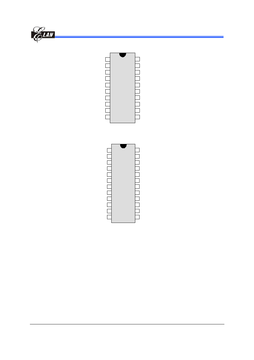
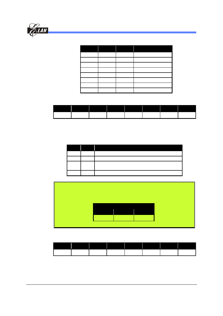
3 Pin Configurations (Package)
3.1 EM78P417NP/M Pin Description
P60/ADC0
P61/ADC1
P62/ADC2
Vss
P63/ADC3
P64/ADC4
P65/ADC5
P66/ADC6
P67/ADC7
P56/TCC
P55/OSCI
P54/OSCO
VDD
P53/PWM3/VREF
P52/PWM2
P51/PWM1
P50/INT
/RESET
EM
78P417NP
EM
78P417NM
1
2
3
4
5
6
7
8
9
18
17
16
15
14
13
12
11
10
Fig. 3-1 Pin Assignment ≠ EM78P417NP/M
EM78P417N/418N/419N
8-Bit Microprocessor with OTP ROM
Product Specification (V1.0) 06.23.2005
∑ 3
(This specification is subject to change without further notice)
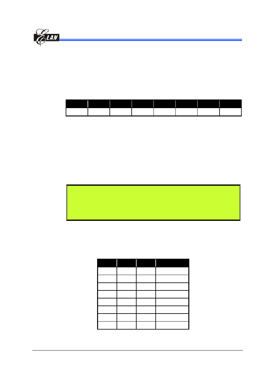
3.2 EM78P418NP/M Pin Description
P70/CIN+
P60/ADC0/CO
P61/ADC1
P62/ADC2
Vss
P63/ADC3
P64/ADC4
P65/ADC5
P66/ADC6
P67/ADC7
P57/CIN-
P56/TCC
P55/OSCI
P54/OSCO
VDD
P53/PWM3/VREF
P52/PWM2
P51/PWM1
P50/INT
/RESET
EM
7
8
P418
NP
EM
7
8
P418
NM
1
2
3
4
5
6
7
8
9
10
20
19
18
17
16
15
14
13
12
11
Fig. 3-2 Pin Assignment ≠ EM78P418NP/M
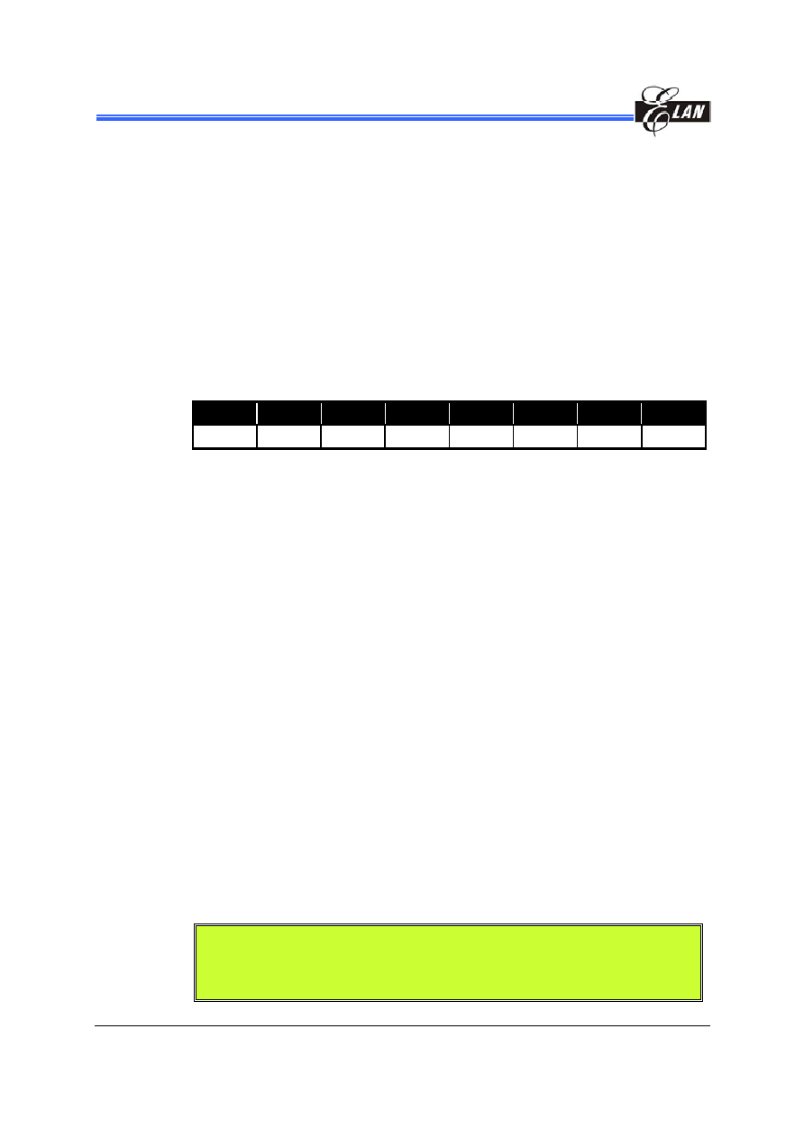
3.3 EM78P419NK/M Pin Description
P70/CIN+
P61/ADC1
P62/ADC2
Vss
P63/ADC3
P64/ADC4
P65/ADC5
P66/ADC6
P67/ADC7
P57/CIN-
P56/TCC
P55/OSCI
P54/OSCO
VDD
P53/PWM3/VREF
P52/PWM2
P51/PWM1
P50/INT
/RESET
EM78P
419
N
K
E
M
78P
419N
M
1
2
3
4
5
6
7
8
9
10
20
19
18
17
16
15
14
13
12
11
P60/ADC0/CO
24
23
22
21
P72
P71
P73
P74
Fig. 3-3 Pin Assignment ≠ EM78P419NK/M
EM78P417N/418N/419N
8-Bit Microprocessor with OTP ROM
4
∑
Product Specification (V1.0) 06.23.2005
(This specification is subject to change without further notice)
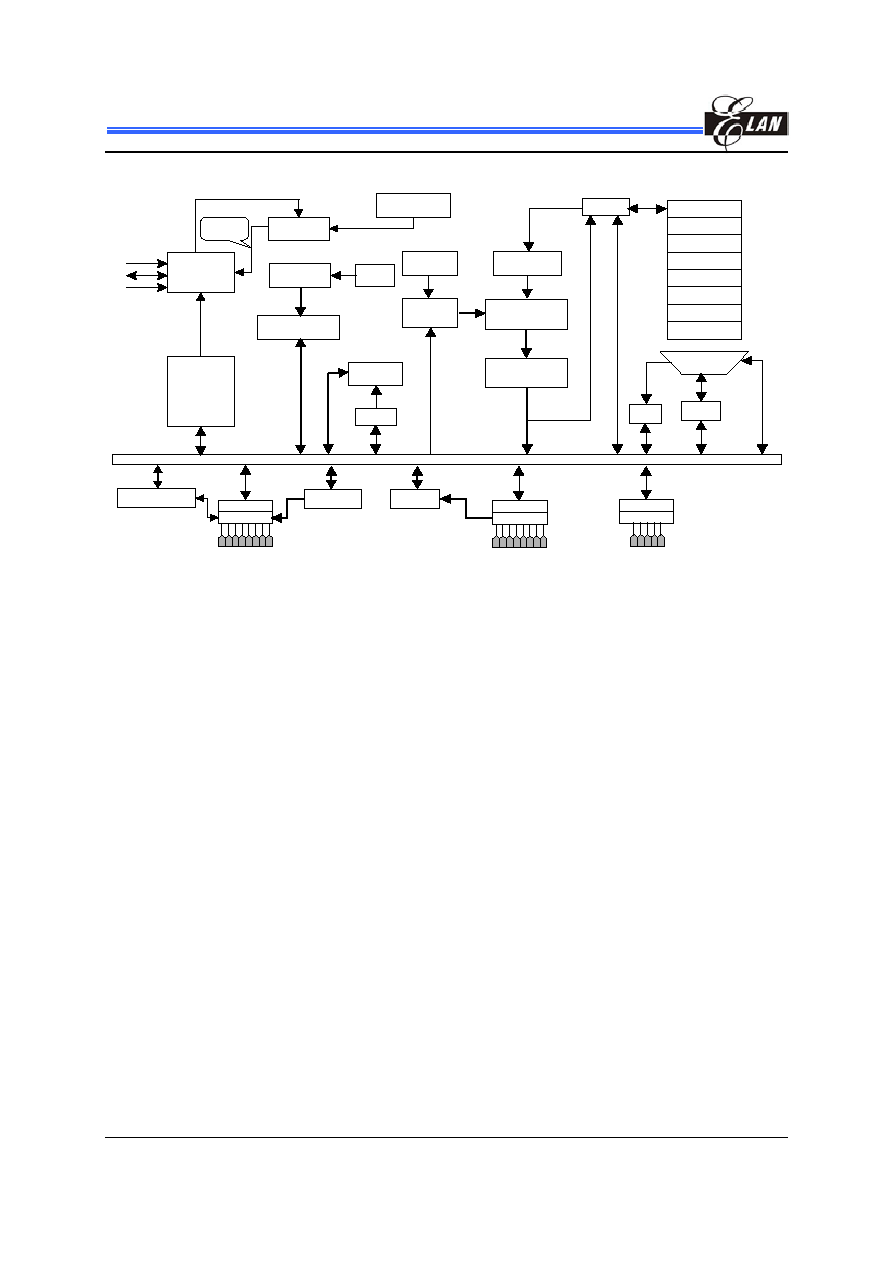
4 Functional Block Diagram
DATA & CO NTROL BUS
IO C 5
R 5
P
5
0
P
5
1
P
5
2
P
5
3
P
5
4
P
5
5
P
5
6
P
5
7
Com parators
12AD C
3 PW M s
IO C6
R 6
P
6
0
P
6
1
P
6
2
P
6
3
P
6
4
P
6
5
P
6
6
P
6
7
ACC
R3
STACK 0
STACK 1
STACK 2
STACK 3
STACK 4
P C
R OM
Instruction
Register
Instruction
D ecoder
ALU
Interrupt
C ontrol
/ INT
R4
R AM
W D T Tim er
Prescaler
O scillator/
Tim m ing
C ontrol
W DT
Time-out
R 1(TC C )
Sleep
&
W ake U p
C ontrol
STACK 5
STACK 6
STACK 7
IO C7
R 7
P
7
0
P
7
1
P
7
2
P
7
3
P
7
4
OSCI
O SCO
/RESET
Prescaler
TC C
Fig. 4-1 EM78P417/8/9N Functional Block Diagram

EM78P417N/418N/419N
8-Bit Microprocessor with OTP ROM
Product Specification (V1.0) 06.23.2005
∑ 5
(This specification is subject to change without further notice)
5 Pin
Description
5.1 EM78P417NP/M Pin Description
Symbol
Pin No. Type
Function
VDD 15
≠
Power
supply
OSCI 17
I
XTAL type Crystal input terminal or external clock input pin
RC type: RC oscillator input pin
OSCO 16
O
XTAL type: Output terminal for crystal oscillator or external clock
input pin
RC type:
Clock output with a duration of one instruction cycle
time. The prescaler is determined by the CONT
register.
External clock signal input
P50 ~ P56
10,12~14,
16 ~ 18
I/O
General-purpose I/O pin
Default value at power-on reset
P60 ~ P67
1 ~ 3,
5 ~ 9
I/O
General-purpose I/O pin
Default value at power-on reset
INT 10
I
External interrupt pin triggered by falling edge
ADC0~ADC7
1 ~ 3,
5 ~ 9
I
Analog to Digital Converter
Defined by ADCON (R9)<0:2>
PWM1,
PWM2,
PWM3
12, 13, 14
O
Pulse width modulation outputs
Defined by PWMCON (IOC80)<5:7>
VREF 14
I
External reference voltage for ADC
Defined by ADCON (R9)<7>
/RESET 11
I
General-purpose Input only
If it remains at logic low, the device will be reset
Wake-up from sleep mode when pin status changes
Voltage on /RESET must not exceed Vdd during normal mode
TCC 18
I
Real time clock/counter with Schmitt trigger input pin. It must be
tied to VDD or VSS if not in use.
VSS 4
≠
Ground.

EM78P417N/418N/419N
8-Bit Microprocessor with OTP ROM
6
∑
Product Specification (V1.0) 06.23.2005
(This specification is subject to change without further notice)
5.2 EM78P418NP/M Pin Description
Symbol
Pin No. Type
Function
VDD 16
≠
Power
supply
OSCI 18
I
XTAL type Crystal input terminal or external clock input pin
RC type: RC oscillator input pin
OSCO 17
O
XTAL type: Output terminal for crystal oscillator or external clock
input pin
RC type:
Clock output with a duration of one instruction cycle
time. The prescaler is determined by the CONT
register.
External clock signal input
P50 ~ P57
11,13~15
17 ~ 20,
I/O
General-purpose I/O pin
Default value at power-on reset
P60 ~ P67
2 ~ 4,
6 ~ 10
I/O
General-purpose I/O pin
Default value at power-on reset
P70 1
I/O
General-purpose I/O pin
Default value at power-on reset
INT 11
I
External interrupt pin triggered by falling edge
ADC0~ADC7
2 ~ 4,
6 ~ 10
I
Analog to Digital Converter
Defined by ADCON (R9)<0:2>
PWM1,
PWM2,
PWM3
13, 14, 15
O
Pulse width modulation outputs
Defined by PWMCON (IOC80)<5:7>
VREF 15
I
External reference voltage for ADC
Defined by ADCON (R9)<7>
CIN-,
CIN+,
CO
20,
1,
2
I
I
O
"≠" ≠> the input pin of Vin≠ of the comparator
"+" ≠> the input pin of Vin+ of the comparator
Pin CO is the output of the comparator
Defined by CMPCON (IOCA0) <0:1>
/RESET 12
I
General-purpose Input only
If it remains at logic low, the device will be reset
Wake-up from sleep mode when pin status changes
Voltage on /RESET must not exceed Vdd during normal mode
TCC 19
I
Real time clock/counter with Schmitt trigger input pin. It must be
tied to VDD or VSS if not in use.
VSS 5
≠
Ground.

EM78P417N/418N/419N
8-Bit Microprocessor with OTP ROM
Product Specification (V1.0) 06.23.2005
∑ 7
(This specification is subject to change without further notice)
5.3 EM78P419NK/M Pin Description
Symbol
Pin No.
Type
Function
VDD 18
-
Power
supply.
OSCI 20
I
XTAL type Crystal input terminal or external clock input pin
RC type: RC oscillator input pin
OSCO 19
O
XTAL type: Output terminal for crystal oscillator or external
clock input pin
RC type:
Clock output with a duration of one instruction
cycle time. The prescaler is determined by the
CONT register.
External clock signal input
P50 ~ P57
13,
15 ~ 17
19 ~ 22,
I/O
General-purpose I/O pin
Default value at power-on reset
P60 ~ P67
4 ~ 6,
8 ~ 12
I/O
General-purpose I/O pin
Default value at power-on reset
P70 ~ P74
3, 2, 1, 24, 23
I/O
General-purpose I/O pin
Default value at power-on reset
INT 13
I
External interrupt pin triggered by falling edge.
ADC0 ~ADC7
4 ~ 6,
8 ~ 12
I
Analog to Digital Converter
Defined by ADCON (R9)<0:2>
PWM1,
PWM2,
PWM3
15, 16, 17
O
Pulse width modulation outputs
Defined by PWMCON (IOC80)<5:7>
VREF 17
I
External reference voltage for ADC
Defined by ADCON (R9)<7>.
CIN≠,
CIN+,
CO
22,
3,
4
I
I
O
"≠" ≠> the input pin of Vin- of the comparator
"+" ≠> the input pin of Vin+ of the comparator
Pin CO is the output of the comparator
Defined by CMPCON (IOCA0) <0:1>
/RESET 14
I
General-purpose Input only
If it remains at logic low, the device will be reset
Wake-up from sleep mode when pin status changes
Voltage on /RESET must not exceed Vdd during normal
mode
TCC 21
I
Real time clock/counter with Schmitt trigger input pin. It must
be tied to VDD or VSS if not in use.
VSS 7
-
Ground.

EM78P417N/418N/419N
8-Bit Microprocessor with OTP ROM
8
∑
Product Specification (V1.0) 06.23.2005
(This specification is subject to change without further notice)
6 Function
Description
6.1 Operational
Registers
6.1.1 R0 (Indirect Address Register)
R0 is not a physically implemented register. Its major function is to perform as an
indirect address pointer. Any instruction using R0 as a pointer, actually accesses the
data pointed by the RAM Select Register (R4).
6.1.2 R1 (Time Clock /Counter)
Increased by an external signal edge through the TCC pin, or by the instruction
cycle clock.
External signal of TCC trigger pulse width must be greater than one instruction.
The signals to increase the counter are determined by Bit 4 and Bit 5 of the CONT
register.
Writable and readable as any other registers.
6.1.3 R2 (Program Counter) and Stack
O n -c h ip P ro g ra m
M e m o ry
A 1 1 A 1 0
R 3
U
s
e
r
Memory
Space
0 0 0 H
0 0 8 H
F F F H
In te rru p t V e c to r
R e s e t V e c to r
A 9 ~ A 0
C A L L
0 0 P A G E 0 0 0 0 0 ~
0 1 P A G E
1 0 P A G E 2 0 8 0 0 ~ 0 B F F
1 1 P A G E 3 0 C 0 0 ~ 0 F F F
R E T
R E T L
R E T I
S ta c k L e v e l 1
0 3 F F
S ta c k L e v e l 3
S ta c k L e v e l 2
1 0 4 0 0 ~ 0 7 F F
S ta c k L e v e l 4
S ta c k L e v e l 5
S ta c k L e v e l 6
S ta c k L e v e l 7
S ta c k L e v e l 8
Fig. 6-1 Program Counter Organization
R2 and hardware stacks are 12-bit wide. The structure is depicted in the table
under Section 6.1.3.1 Data Memory Configuration (next section).
Generates 4K
◊13 bits on-chip ROM addresses to the relative programming
instruction codes. One program page is 1024 words long.
The contents of R2 are all set to "0"s when a RESET condition occurs.

EM78P417N/418N/419N
8-Bit Microprocessor with OTP ROM
Product Specification (V1.0) 06.23.2005
∑ 9
(This specification is subject to change without further notice)
"JMP" instruction allows direct loading of the lower 10 program counter bits. Thus,
"JMP" allows PC to jump to any location within a page.
"CALL" instruction loads the lower 10 bits of the PC, and then PC+1 is pushed into
the stack. Thus, the subroutine entry address can be located anywhere within a
page.
"RET" ("RETL k", "RETI") instruction loads the program counter with the contents
of the top of stack.
"ADD R2, A" allows a relative address to be added to the current PC, and the ninth
and above bits of the PC will increase progressively.
"MOV R2, A" allows loading of an address from the "A" register to the lower 8 bits of
the PC, and the ninth and tenth bits (A8 ~ A9) of the PC will remain unchanged.
Any instruction (except "ADD R2,A") that is written to R2 (e.g., "MOV R2, A", "BC
R2, 6",
) will cause the ninth bit and the tenth bit (A8 ~ A9) of the PC to remain
unchanged.
In the case of EM78P417/8/9N, the most two significant bits (A11 and A10) will be
loaded with the content of PS1 and PS0 in the status register (R3) upon execution
of a "JMP", "CALL", or any other instructions set which write to R2.
All instructions are single instruction cycle (fclk/2 or fclk/4) except for the
instructions that are written to R2. Note that these instructions need one or two
instructions cycle as determined by Code Option Register CYES bit.

EM78P417N/418N/419N
8-Bit Microprocessor with OTP ROM
10
∑
Product Specification (V1.0) 06.23.2005
(This specification is subject to change without further notice)
6.1.3.1 Data Memory Configuration
Address
PAGE Registers
IOC PAGE Registers
IOC PAGE Registers
00
R0 (Indirect Addressing
Register)
Reserve Reserve
01
R1 (Time Clock Counter)
Reserve
Reserve
02
R2 (Program Counter)
Reserve
Reserve
03
R3 (Status Register)
Reserve
Reserve
04
R4 (RAM Select Register)
Reserve
Reserve
05
R5 (Port5)
IOC50 (I/O Port Control
Register)
IOC51 (PRD1: PWM1 time
period)
06
R6 (Port6)
IOC60 (I/O Port Control
Register)
IOC61 (PRD2: PWM2 time
period)
07
R7 (Port7)
IOC70 (I/O Port Control
Register)
IOC71 (PRD3: PWM3 time
period)
08
R8 (ADC Input Select Register) IOC80 (PWM Control Register)
IOC81 (DT1L:Duty cycle of
PWM1)
09
R9 (ADC Control Register)
IOC90 (TIMER Control Register)
IOC91 (DT2L: Duty cycle of
PWM2)
0A
RA (ADC Offset Calibration
Register)
IOCA0
(Comparator Control Register)
IOCA1 (DT3L: Duty cycle of
PWM3)
0B
RB (ADDATA: ADC data
bit11~bit4)
IOCB0
(Pull-down Control Register)
IOCB1 (DTH: Duty cycle of
PWM)
0C
RC (ADDATA1H: ADC data
bit11~bit8)
IOCC0
(Open-drain Control Register)
IOCC1 (TIMER1L: PWM1 timer)
0D
RD (ADDATA1L: ADC data
bit7~bit0)
IOCD0
(Pull-high Control Register)
IOCD1 (TIMER2L: PWM2 timer)
0E
RE (Wake-up Control Register)
IOCE0 (WDT Control Register)
IOCE1 (TIMER3L: PWM3 timer)
0F
RF (Interrupt Status Register)
IOCF0 (Interrupt Mask Register) IOCF1 (TMRH: PWM timer)
10
1F
General Registers
20
3F
Bank 0 Bank 1 Bank 2 Bank 3
EM78P417N/418N/419N
8-Bit Microprocessor with OTP ROM
Product Specification (V1.0) 06.23.2005
∑ 11
(This specification is subject to change without further notice)
6.1.4 R3 (Status Register)
7
6
5
4
3
2
1
0
IOCS PS1 PS0 T
P
Z
DC C
Bit 7 (IOCS): Select the Segment of IO control register.
0 = Segment 0 (IOC50 ~ IOCF0) selected
1 = Segment 1 (IOC51 ~ IOCF1) selected
Bit 6 ~ Bit 5 (PS1 ~ PS0): Page select bits. PS0 ~ PS1 are used to select a program
memory page. When executing a "JMP," "CALL," or other instructions
which cause the program counter to change (e.g., MOV R2, A), PS0 ~
PS1 are loaded into the 11th and 12th bits of the program counter where
it selects one of the available program memory pages. Note that RET
(RETL, RETI) instruction does not change the PS0~PS1 bits. That is,
the return will always be back to the page from where the subroutine was
called, regardless of the current PS0 ~ PS1 bits setting.
PS1
PS0
Program Memory Page [Address]
0
0
Page 0 [000-3FF]
0
1
Page 1 [400-7FF]
1
0
Page 2 [800-BFF]
1
1
Page 3 [C00-FFF]
Bit 4 (T):
Time-out bit. Set to 1 by the "SLEP" and "WDTC" commands, or during
power on and reset to 0 by WDT time-out.
Bit 3 (P):
Power-down bit. Set to 1 during power-on or by a "WDTC" command
and reset to 0 by a "SLEP" command.
NOTE
Bit 4 & Bit 3 (T & P) are read only.
Bit 2 (Z):
Zero flag. Set to "1" if the result of an arithmetic or logic operation is
zero.
Bit 1 (DC): Auxiliary carry flag
Bit 0 (C):
Carry flag
6.1.5 R4 (RAM Select Register)
Bit 7 & Bit 6: are used to select Banks 0 ~ 3.
Bit 5 ~ Bit 0: are used to select registers (address: 00 ~ 3F) in the indirect address
mode.
See the table under Section 6.1.3.1 Data Memory Configuration for the configuration of
the data memory.

EM78P417N/418N/419N
8-Bit Microprocessor with OTP ROM
12
∑
Product Specification (V1.0) 06.23.2005
(This specification is subject to change without further notice)
6.1.6 R5 ~ R7 (Port 5 ~ Port 7)
R5 & R6 are I/O registers.
R7
is I/O registers. The upper 3 bits of R7 are fixed to 0.
6.1.7 R8 (AISR: ADC Input Select Register)
The AISR register defines the pins of Port 6 as analog inputs or as digital I/O,
individually.
7
6
5
4
3
2
1
0
ADE7 ADE6 ADE5 ADE4 ADE3 ADE2 ADE1 ADE0
Bit 7 (ADE7 ): AD converter enable bit of P67 pin
0 = Disable ADC7, P67 acts as I/O pin
1 = Enable ADC7, acts as analog input pin
Bit 6 (ADE6 ): AD converter enable bit of P66 pin
0 = Disable ADC6, P66 acts as I/O pin
1 = Enable ADC6, acts as analog input pin
Bit 5 (ADE5 ): AD converter enable bit of P65 pin
0 = Disable ADC5, P65 acts as I/O pin
1 = Enable ADC5, acts as analog input pin
Bit 4 (ADE4 ): AD converter enable bit of P64 pin
0 = Disable ADC4, P64 acts as I/O pin
1 = Enable ADC4 acts as analog input pin
Bit 3 (ADE3 ): AD converter enable bit of P63 pin
0 = Disable ADC3, P63 acts as I/O pin
1 = Enable ADC3, acts as analog input pin
Bit 2 (ADE2 ): AD converter enable bit of P62 pin
0 = Disable ADC2, P62 acts as I/O pin
1 = Enable ADC2, acts as analog input pin
Bit 1 (ADE1 ): AD converter enable bit of P61 pin
0 = Disable ADC1, P61 acts as I/O pin
1 = Enable ADC1, acts as analog input pin
Bit 0 (ADE0 ): AD converter enable bit of P60 pin.
0 = Disable ADC0, P60 acts as I/O pin
1 = Enable ADC0, acts as analog input pin

EM78P417N/418N/419N
8-Bit Microprocessor with OTP ROM
Product Specification (V1.0) 06.23.2005
∑ 13
(This specification is subject to change without further notice)
NOTE
Note the pin priority of the COS1 and COS0 bits of IOCA0 Control register when
P60/ADE0 acts as analog input or as digital I/O. The Comparator/OP select bits are as
shown in a table under Section 6.2.6, IOCA0 (CMPCON: Comparator Control Register).
The P60/ADE0/CO pin priority is as follows:
6.1.8 R9 (ADCON: ADC Control Register)
7
6
5
4
3
2
1
0
VREFS
CKR1 CKR0 ADRUN
ADPD ADIS2 ADIS1 ADIS0
Bit 7 (VREFS): The input source of the Vref of the ADC
0 = The Vref of the ADC is connected to Vdd (default value), and the
P53/VREF pin carries out the function of P53
1 = The Vref of the ADC is connected to P53/VREF
NOTE
The P53/PWM3/VREF pin cannot be applied to PWM3 and VREF at the same time. If
P53/PWM3/VREF acts as VREF analog input pin, then PWM3E must be "0"..
The P53/PWM3/VREF pin priority is as follows:
Bit 6 & Bit 5 (CKR1 & CKR0): The prescaler of oscillator clock rate of ADC
00 = 1: 4 (default value)
01 = 1: 16
10 = 1: 64
11 = 1: WDT ring oscillator frequency
CKR0:CKR1
Operation Mode
Max. Operation Frequency
00
Fsco/4
1 MHz
01
Fsco/16
4 MHz
10
Fsco/64
16MHz
11
Internal RC
-
P60/ADE0/CO PRIORITY
High
Medium
Low
CO ADE0 P60
P53/PWM3/VREF PIN PRIORITY
High
Medium
Low
VREF PWM3 P53

EM78P417N/418N/419N
8-Bit Microprocessor with OTP ROM
14
∑
Product Specification (V1.0) 06.23.2005
(This specification is subject to change without further notice)
Bit 4 (ADRUN): ADC starts to RUN.
0 = Reset upon completion of the conversion. This bit cannot be
reset through software
1 = an AD conversion is started. This bit can be set by software
Bit 3 (ADPD): ADC Power-down mode
0 = Switch off the resistor reference to save power even while the
CPU is operating
1 = ADC is operating
Bit 2 ~ Bit 0 (ADIS2 ~ADIS0): Analog Input Select
000
=
ADIN0/P60
001
=
ADIN1/P61
010
=
ADIN2/P62
011
=
ADIN3/P63
100
=
ADIN4/P64
101
=
ADIN5/P65
110
=
ADIN6/P66
111
=
ADIN7/P67
These bits can only be changed when the ADIF bit (see Section
6.1.14) and the ADRUN bit are both LOW.
6.1.9 RA (ADOC: ADC Offset Calibration Register)
7
6
5
4
3
2
1
0
CALI
SIGN
VOF[2]
VOF[1]
VOF[0]
"0" "0" "0"
Bit 7 (CALI):
Calibration enable bit for ADC offset
0 = Calibration disable
1 = Calibration enable
Bit 6 (SIGN): Polarity bit of offset voltage
0 = Negative voltage
1 = Positive voltage
Bit 5 ~ Bit 3 (VOF[2] ~ VOF[0]): Offset voltage bits
VOF[2]
VOF[1]
VOF[0]
EM78P417/8/9N
ICE418N
0 0 0
0LSB 0LSB
0 0 1
2LSB 1LSB
0 1 0
4LSB 2LSB
0 1 1
6LSB 3LSB
1 0 0
8LSB 4LSB
1 0 1 10LSB 5LSB
1 1 0 12LSB 6LSB
1 1 1 14LSB 7LSB

EM78P417N/418N/419N
8-Bit Microprocessor with OTP ROM
Product Specification (V1.0) 06.23.2005
∑ 15
(This specification is subject to change without further notice)
Bit 2 ~ Bit 0:
Unimplemented, read as `0'
6.1.10 RB (ADDATA: Converted Value of ADC)
7
6
5
4
3
2
1
0
AD11
AD10 AD9 AD8 AD7 AD6 AD5 AD4
When the AD conversion is completed, the result is loaded into the ADDATA. The
ADRUN bit is cleared, and the ADIF (see Section 6.1.14) is set.
RB is read only.
6.1.11 RC (ADDATA1H: Converted Value of ADC )
7
6
5
4
3
2
1
0
"0" "0" "0" "0"
AD11
AD10
AD9
AD8
When the AD conversion is completed, the result is loaded into the ADDATA1H. The
ADRUN bit is cleared, and the ADIF (see Section 6.1.14) is set.
RC is read only.
6.1.12 RD (ADDATA1L: Converted Value of ADC )
7
6
5
4
3
2
1
0
AD7 AD6 AD5 AD4 AD3 AD2 AD1 AD0
When the AD conversion is completed, the result is loaded into the ADDATA1L. The
ADRUN bit is cleared, and the ADIF (see Section 6.1.14) is set.
RD is read only
6.1.13 RE (WUCR: Wake- Up Control Register)
7
6
5
4
3
2
1
0
EM78P417/8/9N "0" "0" "0" "0"
ADWE CMPWE
ICWE
"0"
ICE418N
Simulator
C3 C2 C1 C0
ADWE CMPWE
ICWE
"0"
Bit 7 ~ Bit 4:
[With EM78P417/8/9N]: Unimplemented, read as `0'.

EM78P417N/418N/419N
8-Bit Microprocessor with OTP ROM
16
∑
Product Specification (V1.0) 06.23.2005
(This specification is subject to change without further notice)
[With Simulator (C3~C0)]: are IRC calibration bits in IRC oscillator mode. Under
IRC oscillator mode of ICE418N simulator, these are the IRC
calibration bits of IRC oscillator mode.
C3
C2
C1
C0
Frequency (MHz)
0 0 0 0 (1-36%)
x
F
0 0 0 1 (1-31.5%)
x
F
0 0 1 0 (1-27%)
x
F
0 0 1 1 (1-22.5%)
x
F
0 1 0 0 (1-18%)
x
F
0 1 0 1 (1-13.5%)
x
F
0 1 1 0 (1-9%)
x
F
0 1 1 1 (1-4.5%)
x
F
1 1 1 1 F
(default)
1 1 1 0 (1+4.5%)
x
F
1 1 0 1 (1+9%)
x
F
1 1 0 0 (1+135%)
x
F
1 0 1 1 (1+18%)
x
F
1 0 1 0 (1+22.5%)
x
F
1 0 0 1 (1+27%)
x
F
1 0 0 0 (1+31.5%)
x
F
1. Frequency values shown are theoretical and taken from an instance of a
high frequency mode. Hence are shown for reference only. Definite
values will depend on the actual process.
2. Similar way of calculation is also applicable to low frequency mode.
Bit 3 (ADWE): ADC wake-up enable bit
0 = Disable ADC wake-up
1 = Enable ADC wake-up
When the ADC Complete is used to enter interrupt vector or to
wake-up EM78P417/8/9N from sleep with AD conversion running, the
ADWE bit must be set to "Enable".
Bit 2 (CMPWE): Comparator wake-up enable bit
0 = Disable Comparator wake-up
1 = Enable Comparator wake-up
When the Comparator output status change is used to enter interrupt
vector or to wake-up EM78P418/9N from sleep, the CMPWE bit must
be set to "Enable".
Bit 1 (ICWE):
Port 6 input change to wake-up status enable bit
0 = Disable Port 6 input change to wake-up status
1 = Enable Port 6 input change wake-up status
When the Port 6 Input Status Change is used to enter interrupt vector
or to wake-up EM78P417/8/9N from sleep, the ICWE bit must be set
to "Enable".
Bit 0:
Not implemented, read as `0'

EM78P417N/418N/419N
8-Bit Microprocessor with OTP ROM
Product Specification (V1.0) 06.23.2005
∑ 17
(This specification is subject to change without further notice)
6.1.14 RF (Interrupt Status Register)
7
6
5
4
3
2
1
0
CMPIF PWM3IF PWM2IF
PWM1IF
ADIF
EXIF
ICIF
TCIF
NOTE
"1" means interrupt request; "0" means no interrupt occurs.
RF can be cleared by instruction but cannot be set.
IOCF0 is the interrupt mask register.
Reading RF will result to "logic AND" of RF and IOCF0.
Bit 7 (CMPIF): Comparator interrupt flag. Set when a change occurs in the output
of Comparator. Reset by software.
Bit 6 (PWM3IF): PWM3 (Pulse Width Modulation) interrupt flag. Set when a selected
duration is reached. Reset by software.
Bit 5 (PWM2IF): PWM2 (Pulse Width Modulation) interrupt flag. Set when a selected
duration is reached. Reset by software.
Bit 4 (PWM1IF): PWM1 (Pulse Width Modulation) interrupt flag. Set when a selected
duration is reached. Reset by software.
Bit 3 (ADIF):
Interrupt flag for analog to digital conversion. Set when AD
conversion is completed. Reset by software.
Bit 2 (EXIF):
External interrupt flag. Set by falling edge on /INT pin. Reset by
software.
Bit 1 (ICIF):
Port 6 input status change interrupt flag. Set when Port 6 input
changes. Reset by software.
Bit 0 (TCIF):
TCC overflow interrupt flag. Set when TCC overflows. Reset by
software.
6.1.15 R10 ~ R3F
All of these are 8-bit general-purpose registers.

EM78P417N/418N/419N
8-Bit Microprocessor with OTP ROM
18
∑
Product Specification (V1.0) 06.23.2005
(This specification is subject to change without further notice)
6.2 Special Purpose Registers
6.2.1 A (Accumulator)
Internal data transfer, or instruction operand holding. It cannot be addressed.
6.2.2 CONT (Control Register)
7
6
5
4
3
2
1
0
INTE INT TS TE PSTE
PST2 PST1 PST0
Bit 7 (INTE): INT signal edge
0 = interrupt occurs at the rising edge on the INT pin
1 = interrupt occurs at the falling edge on the INT pin
Bit 6 (INT): Interrupt enable flag
0 = masked by DISI or hardware interrupt
1 = enabled by the ENI/RETI instructions
This bit is readable only.
Bit 5 (TS): TCC signal source
0 = internal instruction cycle clock. If P56 is used as I/O pin, TS must be
0.
1 = transition on the TCC pin
Bit 4 (TE):
TCC signal edge
0 = increment if the transition from low to high takes place on the TCC
pin
1 = increment if the transition from high to low takes place on the TCC
pin.
Bit 3 (PSTE): Prescaler enable bit for TCC
0 = prescaler disable bit. TCC rate is 1:1.
1 = prescaler enable bit. TCC rate is set as Bit 2 ~ Bit 0.
Bit 2 ~ Bit 0 (PST2 ~ PST0): TCC prescaler bits
PST2
PST1
PST0
TCC Rate
0 0 0
1:2
0 0 1
1:4
0 1 0
1:8
0 1 1 1:16
1 0 0 1:32
1 0 1 1:64
1 1 0 1:128
1 1 1 1:256
EM78P417N/418N/419N
8-Bit Microprocessor with OTP ROM
Product Specification (V1.0) 06.23.2005
∑ 19
(This specification is subject to change without further notice)
NOTE
Tcc timeout period [1/Fosc x prescaler x 256 (Tcc cnt) x 1 (CLK=2)]
Tcc timeout period [1/Fosc x prescaler x 256 (Tcc cnt) x 2 (CLK=4)]
6.2.3 IOC50 ~ IOC70 (I/O Port Control Register)
"1" puts the relative I/O pin into high impedance, while "0" defines the relative I/O pin as
output.
IOC50, IOC60, and IOC70 registers are all readable and writable.
NOTE
Using EM78P417N and EM78P418N type bit9 of the code option register (word0) must
set to "1".Using EM78P417N type must set extra bit7 of IOC50 and bit0 of IOC70 to
"0".Then pin status set to "0".Following the rules will have no addition power
consumption.
6.2.4 IOC80 (PWMCON: PWM Control Register)
7
6
5
4
3
2
1
0
PWM3E
PWM2E
PWM1E
"0" T1EN T1P2 T1P1 T1P0
Bit 7 (PWM3E): PWM3 enable bit
0 = PWM3 is off (default value), and its related pin carries out the P53
function.
1 = PWM3 is on, and its related pin is automatically set to output.
NOTE
The P53/PWM3/VREF pin cannot be applied to PWM3 and VREF at the same time. IF
P53/PWM3/VREF acts as VREF analog input pin, then PWM3E must be "0"..
The P53/PWM3/VREF pin priority is as follows:
P53/PWM3/VREF PIN PRIORITY
High
Medium
Low
VREF PWM3 P53
Bit 6 (PWM2E): PWM2 enable bit
0 = PWM2 is off (default value), and its related pin carries out the P52
function.
1 = PWM2 is on, and its related pin is automatically set to output.

EM78P417N/418N/419N
8-Bit Microprocessor with OTP ROM
20
∑
Product Specification (V1.0) 06.23.2005
(This specification is subject to change without further notice)
Bit 5 (PWM1E): PWM1 enable bit
0 = PWM1 is off (default value), and its related pin carries out the P51
function;
1 = PWM1 is on, and its related pin is automatically set to output.
Bit 4:
Unimplemented, read as `0'
Bit 3 (T1EN):
TMR1 enable bit
0 = TMR1 is off (default value)
1 = TMR1 is on
Bit 2 ~ Bit 0 (T1P2 ~ T1P0): TMR1 clock prescale option bits
T1P2
T1P1
T1P0
Prescale
0 0 0 1:2
(default)
0 0 1 1:4
0 1 0 1:8
0 1 1 1:16
1 0 0 1:32
1 0 1 1:64
1 1 0 1:128
1 1 1 1:256
6.2.5 IOC90 (TMRCON: TIMER Control Register)
7
6
5
4
3
2
1
0
T3EN T2EN T3P2 T3P1 T3P0 T2P2 T2P1 T2P0
Bit 7 (T3EN): TMR3 enable bit
0 = TMR3 is off (default value)
1 = TMR3 is on
Bit 6 (T2EN): TMR2 enable bit
0 = TMR2 is off (default value)
1 = TMR2 is on
Bit 5 ~ Bit 3 (T3P2 ~ T3P0): TMR3 clock prescale option bits
T3P2
T3P1
T3P0
Prescale
0 0 0 1:2(default)
0 0 1 1:4
0 1 0 1:8
0 1 1 1:16
1 0 0 1:32
1 0 1 1:64
1 1 0 1:128
1 1 1 1:256
EM78P417N/418N/419N
8-Bit Microprocessor with OTP ROM
Product Specification (V1.0) 06.23.2005
∑ 21
(This specification is subject to change without further notice)
Bit 2: Bit 0 ( T2P2:T2P0 ): TMR2 clock prescale option bits
T2P2
T2P1
T2P0
Prescale
0 0 0 1:2(default)
0 0 1 1:4
0 1 0 1:8
0 1 1 1:16
1 0 0 1:32
1 0 1 1:64
1 1 0 1:128
1 1 1 1:256
6.2.6 IOCA0 (CMPCON: Comparator Control Register)
7
6
5
4
3
2
1
0
"0" "0" "0" "0" "0"
CPOUT
COS1
COS0
Bit 7 ~ Bit 3: Unimplemented, read as `0'
Bit 2 (CPOUT): the result of the comparator output
Bit 1 ~ Bit 0 (COS1 ~ COS0): Comparator/OP Select bits
COS1 COS0
Function Description
0
0
Comparator and OP not used. P60 acts as normal I/O pin
0
1
Acts as Comparator and P60 acts as normal I/O pin
1 0
Acts as Comparator and P60 acts as Comparator output
pin (CO)
1
1
Acts as OP and P60 acts as OP output pin (CO)
NOTE
The CO and ADEO of the P60/ADE0/CO pins cannot be used at the same time.
The P60/ADE0/CO pin priority is as follows:
P60/ADE0/CO PRIORITY
High
Medium
Low
CO ADE0 P60
6.2.7 IOCB0 (Pull-Down Control Register)
7
6
5
4
3
2
1
0
/PD7 /PD6 /PD5 /PD4 /PD3 /PD2 /PD1 /PD0
IOCB0 register is both readable and writable
Bit 7 (/PD7): Control bit is used to enable the pull-down of the P67 pin
0 = Enable internal pull-down
1 = Disable internal pull-down

EM78P417N/418N/419N
8-Bit Microprocessor with OTP ROM
22
∑
Product Specification (V1.0) 06.23.2005
(This specification is subject to change without further notice)
Bit 6 (/PD6): Control bit is used to enable the pull-down of the P66 pin
Bit 5 (/PD5): Control bit is used to enable the pull-down of the P65 pin
Bit 4 (/PD4): Control bit is used to enable the pull-down of the P64 pin
Bit 3 (/PD3): Control bit is used to enable the pull-down of the P63 pin
Bit 2 (/PD2): Control bit is used to enable the pull-down of the P62 pin
Bit 1 (/PD1): Control bit is used to enable the pull-down of the P61 pin
Bit 0 (/PD0): Control bit is used to enable the pull-down of the P60 pin.
6.2.8 IOCC0 (Open-Drain Control Register)
7
6
5
4
3
2
1
0
/OD7 /OD6 /OD5 /OD4 /OD3 /OD2 /OD1 /OD0
IOCC0 register is both readable and writable.
Bit 7 (OD7): Control bit is used to enable the open-drain of the P57 pin.
0 = Enable open-drain output
1 = Disable open-drain output
Bit 6 (OD6): Control bit is used to enable the open-drain of the P56 pin.
Bit 5 (OD5): Control bit is used to enable the open-drain of the P55 pin.
Bit 4 (OD4): Control bit is used to enable the open-drain of the P54 pin.
Bit 3 (OD3): Control bit is used to enable the open-drain of the P53 pin.
Bit 2 (OD2): Control bit is used to enable the open-drain of the P52 pin.
Bit 1 (OD1): Control bit is used to enable the open-drain of the P51 pin.
Bit 0 (OD0): Control bit is used to enable the open-drain of the P50 pin.
6.2.9 IOCD0 (Pull-high Control Register)
7
6
5
4
3
2
1
0
/PH7 /PH6 /PH5 /PH4 /PH3 /PH2 /PH1 /PH0
IOCD0 register is both readable and writable.
Bit 7 (/PH7): Control bit is used to enable the pull-high of the P67 pin.
0 = Enable internal pull-high;
1 = Disable internal pull-high.
Bit 6 (/PH6): Control bit is used to enable the pull-high of the P66 pin.
Bit 5 (/PH5): Control bit is used to enable the pull-high of the P65 pin.
Bit 4 (/PH4): Control bit is used to enable the pull-high of the P64 pin.
EM78P417N/418N/419N
8-Bit Microprocessor with OTP ROM
Product Specification (V1.0) 06.23.2005
∑ 23
(This specification is subject to change without further notice)
Bit 3 (/PH3): Control bit is used to enable the pull-high of the P53 pin.
Bit 2 (/PH2): Control bit is used to enable the pull-high of the P52 pin.
Bit 1 (/PH1): Control bit is used to enable the pull-high of the P51 pin.
Bit 0 (/PH0): Control bit is used to enable the pull-high of the P50 pin.
6.2.10 IOCE0 (WDT Control Register)
7
6
5
4
3
2
1
0
WDTE EIS PSWE
PSW2 PSW1 PSW0 "0" "0"
Bit 7 (WDTE): Control bit is used to enable Watchdog Timer
0 = Disable WDT
1 = Enable WDT
WDTE is both readable and writable
Bit 6 (EIS):
Control bit is used to define the function of the P50 (/INT) pin
0 = P50, normal I/O pin
1 = /INT, external interrupt pin. In this case, the I/O control bit of P50
(Bit 0 of IOC50) must be set to "1"
NOTE
When EIS is "0," the path of /INT is masked. When EIS is "1," the status of /INT pin
can also be read by way of reading Port 5 (R5). Refer to Fig. 6-4
(I/O Port and I/O
Control Register Circuit for P50(/INT)
) under Section 6.4 (
I/O Ports
).
EIS is both readable and writable.
Bit 5 (PSWE): Prescaler enable bit for WDT
0 = prescaler disable bit. WDT rate is 1:1
1 = prescaler enable bit. WDT rate is set as Bit4~Bit2
Bit 4 ~ Bit 2 (PSW2 ~ PSW0): WDT prescaler bits.
PSW2
PSW1
PSW0
WDT Rate
0 0 0
1:2
0 0 1
1:4
0 1 0
1:8
0 1 1 1:16
1 0 0 1:32
1 0 1 1:64
1 1 0 1:128
1 1 1 1:256
Bit 1 ~ Bit 0: Unimplemented, read as `0'

EM78P417N/418N/419N
8-Bit Microprocessor with OTP ROM
24
∑
Product Specification (V1.0) 06.23.2005
(This specification is subject to change without further notice)
6.2.11 IOCF0 (Interrupt Mask Register)
7
6
5
4
3
2
1
0
CMPIE PWM3IE PWM2IE
PWM1IE
ADIE
EXIE
ICIE
TCIE
NOTE
IOCF0 register is both readable and writable
Individual interrupt is enabled by setting its associated control bit in the IOCF0 to "1."
Global interrupt is enabled by the ENI instruction and is disabled by the DISI
instruction. Refer to Fig. 6-8 (
Interrupt Input Circuit
) under Section 6.6 (
Interrupt
).
Bit 7 (CMPIE): CMPIF interrupt enable bit
0 = Disable CMPIF interrupt
1 = Enable CMPIF interrupt
When the Comparator output status change is used to enter
interrupt vector or to enter next instruction, the CMPIE bit must be
set to "Enable."
Bit 6 (PWM3IE): PWM3IF interrupt enable bit
0 = Disable PWM3 interrupt
1 = Enable PWM3 interrupt
Bit 5 (PWM2IE): PWM2IF interrupt enable bit
0 = Disable PWM2 interrupt
1 = Enable PWM2 interrupt
Bit 4 (PWM1IE): PWM1IF interrupt enable bit
0 = Disable PWM1 interrupt
1 = Enable PWM1 interrupt
Bit 3 (ADIE):
ADIF interrupt enable bit
0 = Disable ADIF interrupt
1 = Enable ADIF interrupt
When the ADC Complete is used to enter interrupt vector or to enter
next instruction, the ADIE bit must be set to "Enable."
Bit 2 (EXIE):
EXIF interrupt enable bit
0 = Disable EXIF interrupt
1 = Enable EXIF interrupt
Bit 1 (ICIE):
ICIF interrupt enable bit
0 = Disable ICIF interrupt
1 = Enable ICIF interrupt
If Port6 Input Status Change Interrupt is used to enter interrupt
vector or to enter next instruction, the ICIE bit must be set to
"Enable."

EM78P417N/418N/419N
8-Bit Microprocessor with OTP ROM
Product Specification (V1.0) 06.23.2005
∑ 25
(This specification is subject to change without further notice)
Bit 0 (TCIE):
TCIF interrupt enable bit.
0 = Disable TCIF interrupt
1 = Enable TCIF interrupt
6.2.12 IOC51 (PRD1: PWM1 Time Period)
The content of IOC51 is the time period (time base) of PWM1. The frequency of PWM1
is the reverse of the period.
6.2.13 IOC61 (PRD2: PWM2 Time Period)
The content of IOC61 is the time period (time base) of PWM2. The frequency of PWM2
is the reverse of the period.
6.2.14 IOC71 (PRD3: PWM3 Time Period)
The content of IOC71 is the time period (time base) of PWM3. The frequency of PWM3
is the reverse of the period.
6.2.15 IOC81 (DT1L: the Least Significant Byte (Bit 7 ~ Bit 0) of
PWM1 Duty Cycle)
A specified value keeps the output of PWM1 to stay high until the value matches with
TMR1.
6.2.16 IOC91 (DT2L: the Least Significant Byte (Bit 7 ~ Bit 0) of
PWM2 Duty Cycle)
A specified value keeps the output of PWM2 to stay high until the value matches with
TMR2.
6.2.17 IOCA1 (DT3L: the Least Significant Byte (Bit 7 ~ Bit 0) of
PWM3 Duty Cycle)
A specified value keeps the output of PWM3 to stay high until the value matches with
TMR3.
6.2.18 IOCB1 (DTH: the Most Significant Bits of PWM Duty Cycle)
7
6
5
4
3
2
1
0
"0" "0"
PWM3[9]
PWM3[8]
PWM2[9]
PWM2[8] PWM1[9] PWM1[8]
Bit 7 & Bit 6:
Unimplemented, read as `0'.
Bit 5 & Bit 4 (PWM3[9], PWM3[8]): The Most Significant Bits of PWM3 Duty Cycle.
Bit 3 & Bit 2 (PWM2[9], PWM2[8]): The Most Significant Bits of PWM2 Duty Cycle.
Bit 1 & Bit 0 (PWM1[9], PWM1[8]): The Most Significant Bits of PWM1 Duty Cycle.
EM78P417N/418N/419N
8-Bit Microprocessor with OTP ROM
26
∑
Product Specification (V1.0) 06.23.2005
(This specification is subject to change without further notice)
6.2.19 IOCC1 (TMR1L: the Least Significant Byte (Bit 7 ~ Bit 0) of
PWM1 Timer)
The content of IOCC1 is read-only.
6.2.20 IOCD1 (TMR2L: the Least Significant Byte (Bit 7 ~ Bit 0) of
PWM2 Timer)
The content of IOCD1 is read-only.
6.2.21 IOCE1 (TMR3L: the Least Significant Byte (Bit 7 ~ Bit 0) of
PWM3 Timer)
The content of IOCE1 is read-only.
6.2.22 IOCF1 (TMRH: the Most Significant Bits of PWM Timer)
7
6
5
4
3
2
1
0
"0" "0"
TMR3[9]
TMR3[8]
TMR2[9]
TMR2[8] TMR1[9] TMR1[8]
The content of IOCF1 is read-only.
Bit 7 & Bit 6:
Unimplemented, read as `0'.
Bit 5 & Bit 4 (TMR3[9], TMR3[8]): The Most Significant Bits of PWM1Timer
Bit 3 & Bit 2 (TMR2[9], TMR2[8]): The Most Significant Bits of PWM2Timer
Bit 1 & Bit 0 (TMR1[9], TMR1[8]): The Most Significant Bits of PWM3Timer
6.3 TCC/WDT and Prescaler
There are two 8-bit counters available as prescalers for the TCC and WDT respectively.
The PST0 ~ PST2 bits of the CONT register are used to determine the ratio of the TCC
prescaler, and the PWR0 ~ PWR2 bits of the IOCE0 register are used to determine the
prescaler of WDT. The prescaler counter is cleared by the instructions each time such
instructions are written into TCC. The WDT and prescaler will be cleared by the
"WDTC" and "SLEP" instructions. Fig. 6-2 (next page) depicts the block diagram of
TCC/WDT.
TCC (R1) is an 8-bit timer/counter. The TCC clock source can be internal clock or
external signal input (edge selectable from the TCC pin). If TCC signal source is from
internal clock, TCC will increase by 1 at every instruction cycle (without prescaler).
Referring to Fig. 6-2, CLK=Fosc/2 or CLK=Fosc/4 is dependent to the CODE Option bit
<CLKS>. CLK=Fosc/2 if the CLKS bit is "0," and CLK=Fosc/4 if the CLKS bit is "1." If
TCC signal source is from external clock input, TCC will increase by 1 at every falling
edge or rising edge of the TCC pin. TCC pin input time length (kept in High or Low
level) must be greater than 1CLK.
NOTE
The internal TCC will stop running when sleep mode occurs. However, during AD
conversion, when TCC is set to "SLEP" instruction, if the ADWE bit of RE register is
enabled, the TCC will keep on running

EM78P417N/418N/419N
8-Bit Microprocessor with OTP ROM
Product Specification (V1.0) 06.23.2005
∑ 27
(This specification is subject to change without further notice)
The watchdog timer is a free running on-chip RC oscillator. The WDT will keep on
running even when the oscillator driver has been turned off (i.e., in sleep mode).
During normal operation or sleep mode, a WDT time-out (if enabled) will cause the
device to reset. The WDT can be enabled or disabled at any time during normal mode
through software programming. Refer to WDTE bit of IOCE0 register (Section 6.2.10
IOCE0 (WDT Control Register). With no prescaler, the WDT time-out duration is
approximately 18ms.
1
8-Bit counter
WDT
Prescaler
8 to 1 MUX
WDT Time out
WDTE
(IOCE0)
TCC Pin
MUX
CLK (Fosc/2 or Fosc/4)
8-Bit Counter (IOCC1)
8 to 1 MUX
TE (CONT)
Data Bus
TCC overflow
interrupt
TS (CONT)
SYNC
2 cycles
TCC (R1)
0
1
PSW2~0
(IOCE0)
Prescaler
PSR2~0
(CONT)
Fig. 6-2 TCC and WDT Block Diagram
6.4 I/O
Ports
The I/O registers (Port 5, Port 6, Port7) are bi-directional tri-state I/O ports. The
Pull-high, Pull-down, and Open-drain functions can be set internally by IOCB0, IOCC0,
and IOCD0 respectively. Port 6 features an input status change interrupt (or wake-up)
function. Each I/O pin can be defined as "input" or "output" pin by the I/O control
registers (IOC50 ~ IOC70). The I/O registers and I/O control registers are both
readable and writable. The I/O interface circuits for Port 5, Port 6, and Port7 are
illustrated in Figures 6-3, 6-4, & 6-5 respectively (see next page). Port 6 with Input
Change Interrupt/Wake-up is shown in Fig. 6-6.
VDD=5V, Setup time period = 16.5ms ± 30%.
VDD=3V, Setup time period = 18ms ± 30%.
1

EM78P417N/418N/419N
8-Bit Microprocessor with OTP ROM
28
∑
Product Specification (V1.0) 06.23.2005
(This specification is subject to change without further notice)
M
U
X
PORT
PCWR
PDWR
IOD
PDRD
0
1
PCRD
D
D
Q
Q
Q
Q
_
_
C
L
C
L
P
R
CLK
CLK
P
R
NOTE: Pull-high and Open-drain are not shown in the figure.
Fig. 6-3 I/O Port and I/O Control Register Circuit for Port 5 and Port7
PCRD
M
U
X
IOD
0
1
INT
PDRD
P50, /INT
Bit 6 of IOCE0
PCWR
D
Q
Q
_
CLK
P
R
C
L
PDWR
D
Q
Q
_
CLK
P
R
C
L
P
R
C
L
CLK
D
Q
Q
_
PORT
TI 0
NOTE: Pull-high and Open-drain are not shown in the figure.
Fig. 6-4 I/O Port and I/O Control Register Circuit for P50(/INT)

EM78P417N/418N/419N
8-Bit Microprocessor with OTP ROM
Product Specification (V1.0) 06.23.2005
∑ 29
(This specification is subject to change without further notice)
PCRD
M
U
X
IOD
0
1
PDRD
P60 ~ P67
PCWR
D
Q
Q
_
CLK
P
R
C
L
PDWR
D
Q
Q
_
CLK
P
R
C
L
P
R
C
L
CLK
D
Q
Q
_
TI n
PORT
NOTE: Pull-high (down) and Open-drain are not shown in the figure.
Fig. 6-5 I/O Port and I/O Control Register Circuit for Port 6
/SLEP
T17
T10
T11
IOCE.1
Interrupt
ENI Instruction
DISI Instruction
Interrupt
(Wake-up from SLEEP)
Next Instruction
(Wake-up from SLEEP)
CLK
CLK
CLK
Q
Q
Q
Q
Q
Q
_
_
_
D
D
D
P
P
P
L
L
L
R
R
R
C
C
C
RE.1
Fig. 6-6 Port 6 Block Diagram with Input Change Interrupt/Wake-up

EM78P417N/418N/419N
8-Bit Microprocessor with OTP ROM
30
∑
Product Specification (V1.0) 06.23.2005
(This specification is subject to change without further notice)
6.4.1 Usage of Port 6 Input Change Wake-up/Interrupt Function
(1) Wake-up
(2) Wake-up and Interrupt
(a) Before SLEEP
(a) Before SLEEP
1. Disable WDT
1. Disable WDT
2. Read I/O Port 6 (MOV R6,R6)
2. Read I/O Port 6 (MOV R6,R6)
3. Execute "ENI" or "DISI"
3. Execute "ENI" or "DISI"
4. Enable wake-up bit (Set RE ICWE =1)
4. Enable wake-up bit (Set RE ICWE =1)
5. Execute "SLEP" instruction
5. Enable interrupt (Set IOCF0 ICIE =1)
(b) After wake-up
6. Execute "SLEP" instruction
Next instruction
(b) After wake-up
1. IF "ENI"
Interrupt vector (008H)
2. IF "DISI"
Next instruction
(3) Interrupt
(a) Before Port 6 pin change
1. Read I/O Port 6 (MOV R6,R6)
2. Execute "ENI" or "DISI"
3. Enable interrupt (Set IOCF0 ICIE =1)
(b) After Port 6 pin changed (interrupt)
1. IF "ENI"
Interrupt vector (008H)
2. IF "DISI"
Next instruction
6.5 RESET and Wake-up
6.5.1 RESET and Wake-up Operation
A RESET is initiated by one of the following events:
1. Power-on reset
2. /RESET pin input "low"
3. WDT time-out (if enabled).
A device is kept in a RESET condition for the duration of approximately 18ms.
2
after the
reset is detected. When in LXT mode, the reset time is 500ms. Once RESET occurs,
the following functions are performed (the initial address is 000h):
The oscillator continues running, or will be started (if under sleep mode)
The Program Counter (R2) is set to all "0"
All I/O port pins are configured as input mode (high-impedance state)
The Watchdog Timer and prescaler are cleared
When power is switched on, the upper 3 bits of R3 and upper 2 bits of R4 are
cleared
The CONT register bits are set to all "1" except for the Bit 6 (INT flag)
VDD=5V, WDT Time-out period = 16.5ms ± 30%.
VDD=3V, WDT Time-out period = 18ms ± 30%.
2

EM78P417N/418N/419N
8-Bit Microprocessor with OTP ROM
Product Specification (V1.0) 06.23.2005
∑ 31
(This specification is subject to change without further notice)
The IOCB0 register bits are set to all "1"
The IOCC0 register bits are set to all "1"
The IOCD0 register bits are set to all "1"
Bit 7 of the IOCE0 register is set to "1", and Bit 6~0 are cleared
Bits 0~6 of RF register and bits 0~6 of IOCF0 register are cleared
Executing the "SLEP" instruction will assert the sleep (power down) mode. While
entering sleep mode, the Oscillator, TCC, TIMER1, TIMER2, and TIMER3 are stopped.
The WDT (if enabled) is cleared but keeps on running.
The controller can be awakened by-
Case 1 External reset input on /RESET pin
Case 2 WDT time-out (if enabled)
Case 3 Port 6 input status changes (if ICWE is enabled)
Case 4 Comparator output status changes (if CMPWE is enabled)
Case 5 AD conversion completed (if ADWE enable).
The first two cases (1 & 2) will cause the EM78P417/8/9N to reset. The T and P flags of
R3 can be used to determine the source of the reset (wake-up). Cases 3, 4, & 5 are
considered the continuation of program execution and the global interrupt ("ENI" or
"DISI" being executed) decides whether or not the controller branches to the interrupt
vector following wake-up. If ENI is executed before SLEP, the instruction will begin to
execute from address 0x8 after wake-up. If DISI is executed before SLEP, the
execution will restart from the instruction next to SLEP after wake-up. All sleep mode
wake up time is150
µs, no matter what the oscillator type or mode is (except when it's in
low XTAL mode). Under low XATL mode, wake up time is 500ms.
Only one of the Cases 1 to 5 can be enabled before entering into sleep mode. That is:
Case [a] If WDT is enabled before SLEP, all of the RE bit is disabled. Hence, the
EM78P417/8/9N can be awaken only with Case 1 or Case 2. Refer to the
section on Interrupt (Section 6.6) for further details.
Case [b] If Port 6 Input Status Change is used to wake -up EM78P417/8/9N and ICWE
bit of RE register is enabled before SLEP, WDT must be disabled. Hence,
the EM78P417/8/9N can be awaken only with Case 3.
Wake-up time is
dependent on oscillator mode. Under RC mode the reset time is 32 clocks
(for oscillator stables).
In High XTAL mode, reset time is 2ms and 32clocks(for oscillator stables);
and in low XTAL mode, the reset time is 500ms.

EM78P417N/418N/419N
8-Bit Microprocessor with OTP ROM
32
∑
Product Specification (V1.0) 06.23.2005
(This specification is subject to change without further notice)
Case [c] If Comparator output status change is used to wake-up EM78P418/9N and
CMPWE bit of RE register is enabled before SLEP, WDT must be disabled by
software. Hence, the EM78P418/9N can be awaken only with Case 4.
Wake-up time is dependent on oscillator mode. Under RC mode the reset
time is 32 clocks (for oscillator stables). In High XTAL mode, reset time is
2ms and 32 clocks (for oscillator stables); and in low XTAL mode, the reset
time is 500ms.
Case [d] If AD conversion completed is used to wake-up EM78P417/8/9N and ADWE
bit of RE register is enabled before SLEP, WDT must be disabled by
software. Hence, the EM78P417/8/9N can be awaken only with Case 5.
The
wake-up time is 15 TAD (ADC clock period).
If Port 6 Input Status Change Interrupt is used to wake up the EM78P417/8/9N (as in
Case b above), the following instructions must be executed before SLEP:
BC R3,
7 ; Select Segment 0
MOV A,
@001110xxb
; Select WDT prescaler and Disable WDT
IOW IOCE0
WDTC
; Clear WDT and prescaler
MOV
R6, R6
; Read Port 6
ENI (or DISI)
; Enable (or disable) global interrupt
MOV
A, @00000x1xb
; Enable Port 6 input change wake-up bit
MOV
RE
MOV
A, @00000x1xb
; Enable Port 6 input change interrupt
IOW
IOCF0
SLEP
; Sleep
Similarly, if the Comparator Interrupt is used to wake up the EM78P418/9N (as in Case
[c] above), the following instructions must be executed before SLEP:
BC R3,
7
; Select Segment 0
MOV A,
@xxxxxx10b
; Select an comparator and P60 act as CO
pin
IOW
IOCA0
MOV A,
@001110xxb
; Select WDT prescaler and Disable WDT
IOW
IOCE0
WDTC
; Clear WDT and prescaler
ENI (or DISI)
; Enable (or disable) global interrupt
MOV
A, @000001xxb ; Enable comparator output status change
wake-up bit
MOV
RE
MOV
A, @000001xxb ; Enable comparator output status change
interrupt
IOW
IOCF0
SLEP
; Sleep

EM78P417N/418N/419N
8-Bit Microprocessor with OTP ROM
Product Specification (V1.0) 06.23.2005
∑ 33
(This specification is subject to change without further notice)
6.5.1.1 Wake-Up and Interrupt Modes Operation Summary
All categories under Wake-up and Interrupt modes are summarized below.
Signal
Sleep Mode
Normal Mode
DISI + IOCF0 (TCIE) bit0=1
Next Instruction+ Set RF (TCIF)=1
ENI + IOCF0 (TCIE) bit0=1
TCC Over Flow
N/A
Interrupt Vector (0x08)+ Set RF (TCIF)=1
RE (ICWE) bit1=0, IOCF0 (ICIE) bit1=0
IOCF0 (ICIE) bit1=0
Oscillator, TCC and TIMERX are stopped.
Port6 input status changed wake-up is invalid.
Port6 input status change interrupted is invalid
RE (ICWE) bit1=0, IOCF0 (ICIE) bit1=1
Set RF (ICIF)=1,
Oscillator, TCC and TIMERX are stopped.
Port6 input status changed wake-up is invalid.
RE (ICWE) bit1=1, IOCF0 (ICIE) bit1=0
Wake-up+ Next Instruction
Oscillator, TCC and TIMERX are stopped.
RE (ICWE) bit1=1, DISI + IOCF0 (ICIE) bit1=1
DISI + IOCF0 (ICIE) bit1=1
Wake-up+ Next Instruction+ Set RF (ICIF)=1
Oscillator, TCC and TIMERX are stopped.
Next Instruction+ Set RF (ICIF)=1
RE (ICWE) bit1=1, ENI + IOCF0 (ICIE) bit1=1
ENI + IOCF0 (ICIE) bit1=1
Port 6 Input Status Change
Wake-up+ Interrupt Vector (0x08)+ Set RF (ICIF)=1
Oscillator, TCC and TIMERX are stopped.
Interrupt Vector (0x08)+ Set RF (ICIF)=1
DISI + IOCF0 (EXIE) bit2=1
Next Instruction+ Set RF (EXIF)=1
ENI + IOCF0 (EXIE) bit2=1
INT Pin
N/A
Interrupt Vector (0x08)+ Set RF (EXIF)=1
RE (ADWE) bit3=0, IOCF0 (ADIE) bit3=0
IOCF0 (ADIE) bit1=0
Clear R9 (ADRUN)=0, ADC is stopped,
AD conversion wake-up is invalid.
Oscillator, TCC and TIMERX are stopped.
AD conversion interrupted is invalid
RE (ADWE) bit3=0, IOCF0 (ADIE) bit3=1
Set RF (ADIF)=1, R9 (ADRUN)=0,
ADC is stopped,
AD conversion wake-up is invalid.
Oscillator, TCC and TIMERX are stopped.
RE (ADWE) bit3=1, IOCF0 (ADIE) bit3=0
Wake-up+ Next Instruction,
Oscillator, TCC and TIMERX keep on running.
Wake-up when ADC completed.
RE (ADWE) bit3=1, DISI + IOCF0 (ADIE) bit3=1
DISI + IOCF0 (ADIE) bit3=1
Wake-up+ Next Instruction+ RF (ADIF)=1,
Oscillator, TCC and TIMERX keep on running.
Wake-up when ADC completed.
Next Instruction+ RF (ADIF)=1
RE (ADWE) bit3=1, ENI + IOCF0 (ADIE) bit3=1
ENI + IOCF0 (ADIE) bit3=1
AD Conversion
Wake-up+ Interrupt Vector (0x08)+ RF (ADIF)=1,
Oscillator, TCC and TIMERX keep on running.
Wake-up when ADC completed.
Interrupt Vector (0x08)+ Set RF (ADIF)=1
DISI + IOCF0 (PWMXIE)=1
Next Instruction+ Set RF (PWMXIF)=1
ENI + IOCF0 (PWMXIE)=1
PWMX (PWM1,PWM2,PWM3)
(When TimerX matches PRDX)
N/A
Interrupt Vector (0x08)+ Set RF (PWMXIF)=1

EM78P417N/418N/419N
8-Bit Microprocessor with OTP ROM
34
∑
Product Specification (V1.0) 06.23.2005
(This specification is subject to change without further notice)
Signal
Sleep Mode
Normal Mode
RE (CMPWE) bit2=0, IOCF0 (CMPIE) bit7=0
IOCF0 (CMPIE) bit7=0
Comparator output status changed wake-up is
invalid.
Oscillator, TCC and TIMERX are stopped.
Comparator output status change interrupted
is invalid.
RE (CMPWE) bit2=0, IOCF0 (CMPIE) bit7=1
Set RF (CMPIF)=1,
Comparator output status changed wake-up is
invalid.
Oscillator, TCC and TIMERX are stopped.
RE (CMPWE) bit2=1, IOCF0 (CMPIE) bit7=0
Wake-up+ Next Instruction,
Oscillator, TCC and TIMERX are stopped.
RE (CMPWE) bit2=1, DISI + IOCF0 (CMPIE)
bit7=1
DISI + IOCF0 (CMPIE) bit7=1
Wake-up+ Next Instruction+ Set RF (CMPIF)=1,
Oscillator, TCC and TIMERX are stopped.
Next Instruction+ Set RF (CMPIF)=1
RE (CMPWE) bit2=1, ENI + IOCF0 (CMPIE)
bit7=1
ENI + IOCF0 (CMPIE) bit7=1
Comparator
(Comparator Output Status
Change)
Wake-up+ Interrupt Vector (0x08)+ Set RF
(CMPIF)=1,
Oscillator, TCC and TIMERX are stopped.
Interrupt Vector (0x08)+ Set RF (CMPIF)=1
WDT Time Out
IOCE (WDTE) Bit7=1
Wake-up+ Reset (address 0x00)
Reset (address 0x00)
6.5.1.2 Register Initial Values after Reset
The following summarizes the initialized values for registers.
Address
Name
Reset Type
Bit 7
Bit 6
Bit 5
Bit 4
Bit 3
Bit 2
Bit 1
Bit 0
Bit Name
C57 C56 C55 C54 C53 C52 C51 C50
Power-on
1 1 1 1 1 1 1 1
/RESET & WDT
1 1 1 1 1 1 1 1
N/A IOC50
Wake-up from
Pin Change
P P P P P P P P
Bit Name
C67
C66
C65
C64
C63 C62 C61 C60
Power-on
1 1 1 1 1 1 1 1
/RESET & WDT
1 1 1 1 1 1 1 1
N/A IOC60
Wake-up from
Pin Change
P P P P P P P P
Bit Name
-
-
-
C74
C73 C72 C71 C70
Power-on
0
0
0
1
1 1 1 1
/RESET & WDT
0
0
0
1
1 1 1 1
N/A IOC70
Wake-up from
Pin Change
P
P
P
P
P P P P
Bit Name
PWM3E PWM2E PWM1E
-
T1EN
T1P2 T1P1 T1P0
Power-on
0
0
0
0
0 0 0 0
/RESET &WDT
0
0
0
0
0 0 0 0
N/A
IOC80
(PWMCON)
Wake-up from
Pin Change
P
P
P
P
P P P P

EM78P417N/418N/419N
8-Bit Microprocessor with OTP ROM
Product Specification (V1.0) 06.23.2005
∑ 35
(This specification is subject to change without further notice)
Address
Name
Reset Type
Bit 7
Bit 6
Bit 5
Bit 4
Bit 3
Bit 2
Bit 1
Bit 0
Bit Name
T3EN
T2EN
T3P2
T3P1
T3P0
T2P2 T2P1 T2P0
Power-on
0
0
0
0
0 0 0 0
/RESET & WDT
0
0
0
0
0 0 0 0
N/A
IOC90
(TMRCON)
Wake-up from
Pin Change
P
P
P
P
P P P P
Bit Name
-
-
-
-
- CPOUT
COS1
COS0
Power-on
0 0 0 0 0 0 0 0
/RESET & WDT
0 0 0 0 0 0 0 0
N/A
IOCA0
(CMPCON)
Wake-up from
Pin Change
P P P P P P P P
Bit Name
/PD7
/PD6
/PD5
/PD4
/PD3
/PD2 /PD1 /PD0
Power-on
1 1 1 1 1 1 1 1
/RESET & WDT
1 1 1 1 1 1 1 1
N/A IOCB0
Wake-up from
Pin Change
P P P P P P P P
Bit Name
/OD7
/OD6
/OD5
/OD4
/OD3
/OD2 /OD1 /OD0
Power-on
1 1 1 1 1 1 1 1
/RESET & WDT
1 1 1 1 1 1 1 1
N/A IOCC0
Wake-up from
Pin Change
P P P P P P P P
Bit Name
/PH7
/PH6
/PH5
/PH4
/PH3
/PH2
/PH1
/PH0
Power-on
1 1 1 1 1 1 1 1
/RESET & WDT
1 1 1 1 1 1 1 1
N/A IOCD0
Wake-up from
Pin Change
P P P P P P P P
Bit Name
WDTE
EIS
PSWE
PSW2
PSW1
PSW0 -
-
Power-on
0 0 0 0 0 0 0 0
/RESET & WDT
0 0 0 0 0 0 0 0
N/A IOCE0
Wake-up from
Pin Change
P P P P P P P P
Bit Name
CMPIE
PMW3IE PMW2IE PWM1IE
ADIE
EXIE ICIE TCIE
Power-on
0 0 0 0 0 0 0 0
/RESET & WDT
0 0 0 0 0 0 0 0
N/A IOCF0
Wake-up from
Pin Change
P P P P P P P P
Bit Name
PRD1[7] PRD1[6] PRD1[5] PRD1[4] PRD1[3] PRD1[2] PRD1[1] PRD1[0]
Power-on
0 0 0 0 0 0 0 0
/RESET & WDT
0 0 0 0 0 0 0 0
N/A
IOC51
(PRD1)
Wake-up from
Pin Change
P P P P P P P P

EM78P417N/418N/419N
8-Bit Microprocessor with OTP ROM
36
∑
Product Specification (V1.0) 06.23.2005
(This specification is subject to change without further notice)
Address
Name
Reset Type
Bit 7
Bit 6
Bit 5
Bit 4
Bit 3
Bit 2
Bit 1
Bit 0
Bit Name
PRD2[7] PRD2[6] PRD2[5] PRD2[4] PRD2[3] PRD2[2] PRD2[1] PRD2[0]
Power-on
0 0 0 0 0 0 0 0
/RESET & WDT
0 0 0 0 0 0 0 0
N/A
IOC61
(PRD2)
Wake-up from
Pin Change
P P P P P P P P
Bit Name
PRD3[7] PRD3[6] PRD3[5] PRD3[4] PRD3[3] PRD3[2] PRD3[1] PRD3[0]
Power-on
0 0 0 0 0 0 0 0
/RESET & WDT
0 0 0 0 0 0 0 0
N/A
IOC71
(PRD3)
Wake-up from
Pin Change
P P P P P P P P
Bit Name
DT1[7] DT1[6] DT1[5] DT1[4] DT1[3] DT1[2] DT1[1] DT1[0]
Power-on
0 0 0 0 0 0 0 0
/RESET & WDT
0 0 0 0 0 0 0 0
N/A
IOC81
(DT1L)
Wake-up from
Pin Change
P P P P P P P P
Bit Name
DT2[7] DT2[6] DT2[5] DT2[4] DT2[3] DT2[2] DT2[1] DT2[0]
Power-on
0 0 0 0 0 0 0 0
/RESET & WDT
0 0 0 0 0 0 0 0
N/A
IOC91
(DT2L)
Wake-up from
Pin Change
P P P P P P P P
Bit Name
DT3[7] DT3[6] DT3[5] DT3[4] DT3[3] DT3[2] DT3[1] DT3[0]
Power-on
0 0 0 0 0 0 0 0
/RESET & WDT
0 0 0 0 0 0 0 0
N/A
IOCA1
(DT3L)
Wake-up from
Pin Change
P P P P P 0 P P
Bit Name
- -
DT3[9] DT3[8] DT2[9] DT2[8] DT1[9] DT1[8]
Power-on
0 0 0 0 0 0 0 0
/RESET & WDT
0 0 0 0 0 0 0 0
N/A
IOCB1
(DT1H,
2H, 3H)
Wake-up from
Pin Change
P P P P P P P P
Bit Name
TMR1[7] TMR1[6] TMR1[5] TMR1[4] TMR1[3] TMR1[2] TMR1[1] TMR1[0]
Power-on
0 0 0 0 0 0 0 0
/RESET & WDT
0 0 0 0 0 0 0 0
N/A
IOCC1
(TMR1L)
Wake-up from
Pin Change
P P P P P P P P
Bit Name
TMR2[7] TMR2[6] TMR2[5] TMR2[4] TMR2[3] TMR2[2] TMR2[1] TMR2[0]
Power-on
0 0 0 0 0 0 0 0
/RESET & WDT
0 0 0 0 0 0 0 0
N/A
IOCD1
(TMR2L)
Wake-up from
Pin Change
P P P P P P P P

EM78P417N/418N/419N
8-Bit Microprocessor with OTP ROM
Product Specification (V1.0) 06.23.2005
∑ 37
(This specification is subject to change without further notice)
Address
Name
Reset Type
Bit 7
Bit 6
Bit 5
Bit 4
Bit 3
Bit 2
Bit 1
Bit 0
Bit Name
TMR3[7] TMR3[6] TMR3[5] TMR3[4] TMR3[3] TMR3[2] TMR3[1] TMR3[0]
Power-on
0 0 0 0 0 0 0 0
/RESET & WDT
0 0 0 0 0 0 0 0
N/A
IOCE1
(TMR3L)
Wake-up from
Pin Change
P P P P P P P P
Bit Name
- -
TMR3[9] TMR3[8] TMR2[9] TMR2[8] TMR1[9] TMR1[8]
Power-on
0 0 0 0 0 0 0 0
/RESET & WDT
0 0 0 0 0 0 0 0
N/A
IOCF1
(TMR1H,
2H, 3H)
Wake-up from
Pin Change
P P P P P P P P
Bit Name
INTE
INT
TS
TE
PSTE
PST2 PST1 PST0
Power-on
0 0 0 0 0 0 0 0
/RESET & WDT
0 0 0 0 0 0 0 0
N/A CONT
Wake-up from
Pin Change
P P P P P P P P
Bit Name
- - - - - - - -
Power-on
U U U U U U U U
/RESET & WDT
P P P P P P P P
0x00 R0(IAR)
Wake-up from
Pin Change
P P P P P P P P
Bit Name
- - - - - - - -
Power-on
0 0 0 0 0 0 0 0
/RESET & WDT
0 0 0 0 0 0 0 0
0x01 R1(TCC)
Wake-up from
Pin Change
P P P P P P P P
Bit Name
- - - - - - - -
Power-on
0 0 0 0 0 0 0 0
/RESET & WDT
0 0 0 0 0 0 0 0
0x02 R2(PC)
Wake-up from Pi
Change
Jump to address 0x08 or continue to execute next instruction
Bit Name
IOCS
PS1
PS0
T
P
Z
DC
C
Power-on
0 0 0 1 1 U U U
/RESET & WDT
0 0 0 t t P P P
0x03 R3(SR)
Wake-up from
Pin Change
P P P t t P P P
Bit Name
BS7
BS6
-
- - - - -
Power-on
0 0 U U U U U U
/RESET & WDT
0 0 P P P P P P
0x04 R4(RSR)
Wake-up from
Pin Change
P P P P P P P P

EM78P417N/418N/419N
8-Bit Microprocessor with OTP ROM
38
∑
Product Specification (V1.0) 06.23.2005
(This specification is subject to change without further notice)
Address
Name
Reset Type
Bit 7
Bit 6
Bit 5
Bit 4
Bit 3
Bit 2
Bit 1
Bit 0
Bit Name
P57 P56 P55 P54 P53 P52 P51 P50
Power-on
1 1 1 1 1 1 1 1
/RESET & WDT
1 1 1 1 1 1 1 1
0x05 R5
Wake-up from
Pin Change
P P P P P P P P
Bit Name
P67
P66
P65
P64
P63 P62 P61 P60
Power-on
1 1 1 1 1 1 1 1
/RESET & WDT
1 1 1 1 1 1 1 1
0x06 P6
Wake-up from
Pin Change
P P P P P P P P
Bit Name
-
-
- P74 P73 P72 P71 P70
Power-on
0 0 0 1 1 1 1 1
/RESET & WDT
0 0 0 1 1 1 1 1
0x7 R7
Wake-up from
Pin Change
P P P P P P P P
Bit Name
ADE7
ADE6
ADE5
ADE4
ADE3
ADE2 ADE1 ADE0
Power-on
0 0 0 0 0
0
0
0
/RESET & WDT
0 0 0 0 0
0
0
0
0x8
R8
(AISR)
Wake-up from
Pin Change
P P P P P
P
P
P
Bit Name
VREFS CKR1
CKR0 ADRUN ADPD
ADIS2 ADIS1 ADIS0
Power-on
0 0 0 0 0 0 0 0
/RESET and WDT
0 0 0 0 0 0 0 0
0x9
R9
(ADCON)
Wake-up from
Pin Change
P P P P P P P P
Bit Name
CALI
SIGN
VOF[2] VOF[1] VOF[0]
- - -
Power-on
0 0 0 0 0 0 0 0
/RESET and WDT
0 0 0 0 0 0 0 0
0xA
RA
(ADOC)
Wake-up from
Pin Change
P P P P P P P P
Bit Name
AD11
AD10
AD9
AD8
AD7
AD6
AD5
AD4
Power-on
U U U U U U U U
/RESET and WDT
U U U U U U U U
0xB
RB
(ADDDATA)
Wake-up from
Pin Change
P P P P P P P P
Bit Name
- - - -
AD11
AD10
AD9
AD8
Power-on
0 0 0 0 U U U U
/RESET and WDT
0 0 0 0 U U U U
0xC
RC
(ADDATA1H)
Wake-up from
Pin Change
P P P P P P P P

EM78P417N/418N/419N
8-Bit Microprocessor with OTP ROM
Product Specification (V1.0) 06.23.2005
∑ 39
(This specification is subject to change without further notice)
Address
Name
Reset Type
Bit 7
Bit 6
Bit 5
Bit 4
Bit 3
Bit 2
Bit 1
Bit 0
Bit Name
AD7
AD6
AD5
AD4
AD3
AD2
AD1
AD0
Power-on
U U U U U U U U
/RESET and WDT
U U U U U U U U
0xD
RD
(ADDATA1L)
Wake-up from
Pin Change
P P P P P P P P
Bit Name
- - - -
ADWE CMPWE ICWE
-
Power-on
0 0 0 0 0 0 0 0
/RESET and WDT
0 0 0 0 0 0 0 0
0xE
RE
(WUCR)
Wake-up from
Pin Change
P P P P P P P P
Bit Name
CMPIF PWM3IF PWM2IF PWM1IF ADIF
EXIF
ICIF
TCIF
Power-on
0 0 0 0 0 0 0 0
/RESET and WDT
0 0 0 0 0 0 0 0
0xF
RF
(ISR)
Wake-up from
Pin Change
P P P P P P P P
Bit Name
- - - - - - - -
Power-on
U U U U U U U U
/RESET and WDT
P P P P P P P P
0x10 ~
0x3F
R10 ~ R3F
Wake-up from
Pin Change
P P P P P P P P
LEGEND: ≠
: not used.
U: unknown or don't care
t: check "Reset Type" table in Section 6.5.2
P:
previous value before reset
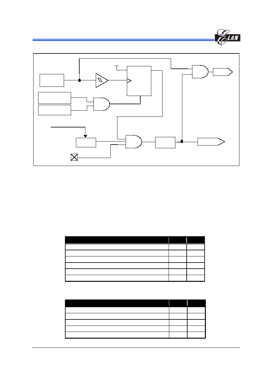
EM78P417N/418N/419N
8-Bit Microprocessor with OTP ROM
40
∑
Product Specification (V1.0) 06.23.2005
(This specification is subject to change without further notice)
6.5.1.3 Controller Reset Block Diagram
W DT Timeout
Oscillator
D Q
CLK
CLR
WDT
VDD
Setup time
Reset
CLK
/RESET
Power-On Reset
Voltage Detector
WTE
Fig. 6-7 Controller Reset Block Diagram
6.5.2 The T and P Status under STATUS Register
A RESET condition is initiated by one of the following events:
1. Power-on reset
2. /RESET pin input "low"
3. WDT time-out (if enabled).
The values of T and P as listed in the table below, are used to check how the processor
wakes up.
Reset Type
T
P
Power-on 1
1
/RESET during Operating mode
*
P
*
P
/RESET wake-up during SLEEP mode
1
0
WDT during Operating mode
0
*
P
WDT wake-up during SLEEP mode
0
0
Wake-up on pin change during SLEEP mode
1
0
*
P: Previous status before reset
The following shows the events that may affect the status of T and P.
Event
T
P
Power-on 1
1
WDTC instruction
1
1
WDT time-out
0
*
P
SLEP instruction
1
0
Wake-up on pin changed during SLEEP mode
1
0
*
P: Previous value before reset

EM78P417N/418N/419N
8-Bit Microprocessor with OTP ROM
Product Specification (V1.0) 06.23.2005
∑ 41
(This specification is subject to change without further notice)
6.6 Interrupt
The EM78P417/8/9N has six interrupts as listed below:
1. TCC overflow interrupt
2. Port 6 Input Status Change Interrupt
3. External interrupt [(P50, /INT) pin]
4. Analog to Digital conversion completed
5. When TMR1/TMR2/TIMER3 matches with PRD1/PRD2/PRD3 respectively in PWM
6. When the comparators output changes (for EM78P418/9N only)
Before the Port 6 Input Status Change Interrupt is enabled, reading Port 6 (e.g., "MOV
R6, R6") is necessary. Each Port 6 pin will have this feature if its status changes. Any
pin configured as output, including the P50 pin configured as /INT, is excluded from this
function. Port 6 Input Status Change Interrupt will wake up the EM78P417/8/9N from
sleep mode if it is enabled prior to going into the sleep mode by executing SLEP. When
wake-up occurs, the controller will continue to execute the succeeding program if the
global interrupt is disabled. If enabled, it will branch out to the interrupt vector 008H.
External interrupt equipped with digital noise rejection circuit (input pulse less than 8
system clocks time) is eliminated as noise. Edge selection is possible with /INT. Refer
to the Word 1 Bits 8~7 (Section 6.14.2, Code Option Register (Word 1)) for digital noise
rejection definition.
RF is the interrupt status register that records the interrupt requests in the relative
flags/bits. IOCF0 is an interrupt mask register. The global interrupt is enabled by the
ENI instruction and is disabled by the DISI instruction. When one of the interrupts
(when enabled) occurs, the next instruction will be fetched from address 008H. Once in
the interrupt service routine, the source of an interrupt can be determined by polling the
flag bits in RF. The interrupt flag bit must be cleared by instructions before leaving the
interrupt service routine to avoid recursive interrupts.
The flag (except ICIF bit) in the Interrupt Status Register (RF) is set regardless of the
status of its mask bit or of the ENI execution. Note that the result of RF will be the logic
AND of RF and IOCF0 (refer to figure below). The RETI instruction ends the interrupt
routine and enables the global interrupt (the ENI execution).

EM78P417N/418N/419N
8-Bit Microprocessor with OTP ROM
Fig. 6-8 Interrupt Input Circuit
6.7 Analog-To-Digital Converter (ADC)
The analog-to-digital circuitry consists of an 8-bit analog multiplexer; three control
registers (AISR/R8, ADCON/R9, & ADOC/RA), three data registers (ADDATA1/RB,
ADDATA1H/RC, & ADDATA1L/RD) and an ADC with 12-bit resolution as shown in the
functional block diagram below. The analog reference voltage (Vref) and the analog
ground are connected via separate input pins.
The ADC module utilizes successive approximation to convert the unknown analog
signa
TA1H and
ADDATA1L. Input channels are selected by the analog input multiplexer via the
ADCON register Bits.
l into a digital value. The result is fed to the ADDATA, ADDA
ADDATA1H
DATA BUS
ADC3
ADC2
ADC1
ADC0
ADC4
ADC5
ADC6
ADC7
Vref
Power-Down
Fsco
Internal RC
4-1
MUX
7 ~ 0
3
4
ADC
( successive approximation )
3
5
6
ADCON
RF
AISR
ADCON
Start to Convert
0
1
2
ADCON
8
-
1
A
n
a
l
o
g
S
w
i
t
c
h
0
1
2
3
4
5
6
7
8
9
10
11
ADDATA1L
Fig. 6-9 Analog-to-Digital Conversion Functional Block Diagram
42
∑
Product Specification (V1.0) 06.23.2005
(This specification is subject to change without further notice)

EM78P417N/418N/419N
8-Bit Microprocessor with OTP ROM
Product Specification (V1.0) 06.23.2005
∑ 43
(This specification is subject to change without further notice)
6.7.1 ADC Control Register (AISR/R8, ADCON/R9, ADOC/RA)
6.7.1.1 R8 (AISR: ADC Input Select Register)
7
6
5
4
3
2
1
0
SYMBOL
ADE7 ADE6 ADE5 ADE4 ADE3 ADE2 ADE1
*Init_Value
0 0 0 0 0 0 0
AISR register defines the Port 6 pins as analog inputs or as digital I/O, individually.
Bit 7 (ADE7 ): AD converter enable bit of P67 pin
0 = Disable ADC7, P67 acts as I/O pin
1 = Enable ADC7 acts as analog input pin
Bit 6 (ADE6 ): AD converter enable bit of P66 pin
0 = Disable ADC6, P66 acts as I/O pin
1 = Enable ADC6 acts as analog input pin
Bit 5 (ADE5 ): AD converter enable bit of P65 pin
0 = Disable ADC5, P65 acts as I/O pin
1 = Enable ADC5 acts as analog input pin
Bit 4 (ADE4 ): AD converter enable bit of P64 pin
0 = Disable ADC4, P64 acts as I/O pin
1 = Enable ADC4 acts as analog input pin
Bit 3 (ADE3 ): AD converter enable bit of P63 pin
0 = Disable ADC3, P63 acts as I/O pin
1 = Enable ADC3 acts as analog input pin
Bit 2 (ADE2 ): AD converter enable bit of P62 pin
0 = Disable ADC2, P63 acts as I/O pin
1 = Enable ADC2 acts as analog input pin
Bit 1 (ADE1 ): AD converter enable bit of P61 pin
0 = Disable ADC1, P61 acts as I/O pin
1 = Enable ADC1 acts as analog input pin

EM78P417N/418N/419N
8-Bit Microprocessor with OTP ROM
44
∑
Product Specification (V1.0) 06.23.2005
(This specification is subject to change without further notice)
Bit 0 (ADE0 ): AD converter enable bit of P60 pin
0 = Disable ADC0, P60 acts a s I/O pin
1 = Enable ADC0 acts as analog input pin
NOTE
Note the pin priority of the COS1 and COS0 bits of IOCA0 Control register when
P60/ADE0 acts as analog input or as digital I/O. The Comparator/OP select bits are as
shown in a table under Section 6.2.6.
The P60/ADE0/CO pin priority is as follows:
6.7.1.2 R9 (ADCON: ADC Control Register)
Bit
7
6
5
4
3
2
1
0
SYMBOL VREFS CKR1
CKR0
ADRUN
ADPD
ADIS2 ADIS1 ADIS0
*
Init_Value
0 0 0 0 0 0 0 0
*
Init_Value: Initial value at power on reset
ADCON register controls the operation of the AD conversion and decides which pin
should be currently active.
Bit 7(VREFS): The input source of the Vref of the ADC
0 = The Vref of the ADC is connected to Vdd (default value), and the
P53/VREF pin carries out the function of P53
1 = The Vref of the ADC is connected to P53/VREF
NOTE
The P53/PWM3/VREF pin cannot be applied to PWM3 and VREF at the same time. IF
P53/PWM3/VREF acts as VREF analog input pin, then PWM3E must be "0"..
The P53/PWM3/VREF pin priority is as follows:
P60/ADE0/CO PRIORITY
High
Medium
Low
CO ADE0 P60
P53/PWM3/VREF PIN PRIORITY
High
Medium
Low
VREF PWM3 P53

EM78P417N/418N/419N
8-Bit Microprocessor with OTP ROM
Product Specification (V1.0) 06.23.2005
∑ 45
(This specification is subject to change without further notice)
Bit 6 ~ Bit 5 (CKR1 ~ CKR0): The prescaler oscillator clock rate of ADC
00 = 1: 4 (default value)
01 = 1: 16
10 = 1: 64
11 = 1: WDT ring oscillator frequency
CKR0:CKR1 Operation Mode Max. Operation Frequency
00
Fsco/4
1 MHz
01
Fsco/16
4 MHz
10
Fsco/64
16MHz
11
Internal RC
-
Bit 4 (ADRUN):
ADC starts to RUN.
0 = reset on completion of the conversion. This bit
cannot be reset though software.
1 = an AD conversion is started. This bit can be set by
software.
Bit 3 (ADPD):
ADC Power-down mode.
0 = switch off the resistor reference to save power even
while the CPU is operating.
1 = ADC is operating
Bit 2 ~ Bit 0 (ADIS2 ~ ADIS0): Analog Input Select.
000
=
AN0/P60
001
=
AN1/P61
010
=
AN2/P62
011
=
AN3/P63
100
=
AN4/P64
101
=
AN5/P65
110
=
AN6/P66
111
=
AN7/P67
These bits can only be changed when the ADIF bit and
the ADRUN bit are both LOW.
EM78P417N/418N/419N
8-Bit Microprocessor with OTP ROM
46
∑
Product Specification (V1.0) 06.23.2005
(This specification is subject to change without further notice)
6.7.1.3 RA (ADOC: ADC Offset Calibration Register)
7
6
5
4
3
2
1
0
CALI
SIGN
VOF[2]
VOF[1]
VOF[0]
"0" "0" "0"
Bit 7 (CALI): Calibration enable bit for ADC offset
0 = Calibration disable;
1 = Calibration enable.
Bit 6 (SIGN): Polarity bit of offset voltage
0 = Negative voltage;
1 = Positive voltage.
Bit 5 ~ Bit 3 (VOF[2] ~ VOF[0]): Offset voltage bits.
VOF[2]
VOF[1]
VOF[0]
EM78P417/8/9N
ICE418N
0 0 0
0LSB 0LSB
0 0 1
2LSB 1LSB
0 1 0
4LSB 2LSB
0 1 1
6LSB 3LSB
1 0 0
8LSB 4LSB
1 0 1 10LSB 5LSB
1 1 0 12LSB 6LSB
1 1 1 14LSB 7LSB
Bit 2 ~ Bit 0: Unimplemented, read as `0'.
6.7.2 ADC Data Register (ADDATA/RB, ADDATA1H/RC,
ADDATA1L/RD)
When the AD conversion is completed, the result is loaded to the ADDATA, ADDATA1H
and ADDATA1L registers. The ADRUN bit is cleared, and the ADIF is set.
6.7.3 ADC Sampling Time
The accuracy, linearity, and speed of the successive approximation of AD converter are
dependent on the properties of the ADC and the comparator. The source impedance
and the internal sampling impedance directly affect the time required to charge the
sample holding capacitor. The application program controls the length of the sample
time to meet the specified accuracy. Generally speaking, the program should wait for
2
µs for each K of the analog source impedance and at least 2µs for the
low-impedance source. The maximum recommended impedance for analog source is
10K
at Vdd=5V. After the analog input channel is selected, this acquisition time must
be done before the conversion is started.

EM78P417N/418N/419N
8-Bit Microprocessor with OTP ROM
Product Specification (V1.0) 06.23.2005
∑ 47
(This specification is subject to change without further notice)
6.7.4 AD Conversion Time
CKR0 and CKR1 select the conversion time (Tct), in terms of instruction cycles. This
allows the MCU to run at the maximum frequency without sacrificing the AD conversion
accuracy. For the EM78P417/8/9N, the conversion time per bit is about 4
µs. The table
below shows the relationship between Tct and the maximum operating frequencies.
CKR0:CKR1
Operation
Mode
Max. Operation
Frequency
Max. Conversion
Rate/Bit
Max. Conversion Rate
00 Fsco/4 1
MHz
250kHz (4us)
15*4us=60us(16.7kHz)
01 Fsco/16 4MHz
250kHz (4us)
15*4us=60us(16.7kHz)
10
Fsco/64
16MHz
250kHz( 4us)
15*4us=60us(16.7kHz)
11
Internal RC
-
14kHz (71us)
15*71us=1065us(0.938kHz)
NOTE
Pin not used as an analog input pin can be used as regular input or output pin.
During conversion, do not perform output instruction to maintain precision for all of
the pins.
6.7.5 ADC Operation during Sleep Mode
In order to obtain a more accurate ADC value and reduce power consumption, the AD
conversion remains operational during sleep mode. As the SLEP instruction is
executed, all the MCU operations will stop except for the Oscillator, TCC, TIMER1,
TIMER2, TIMER3, and AD conversion.
The AD Conversion is considered completed as determined by:
1. ADRUN bit of R9 register is cleared ("0" value)
2. Wake-up from AD conversion (where it remains in operation during sleep mode)
The results are fed into the ADDATA, ADDATA1H, and ADDATA1L registers when the
conversion is completed. If the ADWE is enabled, the device will wake up. Otherwise,
the AD conversion will be shut off, no matter what the status of ADPD bit is.
6.7.6 Programming Process/Considerations
6.7.6.1 Programming Process
Follow these steps to obtain data from the ADC:
1. Write to the eight bits (ADE7:ADE0) on the R8 (AISR) register to define the
characteristics of R6 (digital I/O, analog channels, or voltage reference pin)
2. Write to the R9/ADCON register to configure AD module:
a) Select ADC input channel ( ADIS2:ADIS0 )
b) Define AD conversion clock rate ( CKR1:CKR0 )
c) Select the VREFS input source of the ADC
d) Set the ADPD bit to 1 to begin sampling

EM78P417N/418N/419N
8-Bit Microprocessor with OTP ROM
48
∑
Product Specification (V1.0) 06.23.2005
(This specification is subject to change without further notice)
3. Set the ADWE bit, if the wake-up function is employed
4. Set the ADIE bit, if the interrupt function is employed
5. Write "ENI" instruction, if the interrupt function is employed
6. Set the ADRUN bit to 1
7. Write "SLEP" instruction or Polling.
8. Wait for wake-up or for ADRUN bit to be cleared ("0" value)
9. Read the ADDATA or ADDATA1H and ADDATA1L conversion data registers. If
ADC input channel changes at this time, the ADDATA, ADDATA1H, and
ADDATA1L values can be cleared to `0'.
10. Clear the interrupt flag bit (ADIF).
11. For next conversion, go to Step 1 or Step 2 as required. At least 2 Tct is required
before the next acquisition starts.
NOTE
In order to obtain accurate values, it is necessary to avoid any data transition on I/O
pins during AD conversion
6.7.6.2 Sample Demo Programs
A. Define a General Registers
R_0 == 0
; Indirect addressing register
PSW == 3
; Status register
PORT5 == 5
PORT6 == 6
RE== 0XE
; Wake-up control resister
RF== 0XF
; Interrupt status register
B. Define a Control Register
IOC50 == 0X5
; Control Register of Port 5
IOC60 == 0X6
; Control Register of Port 6
C_INT== 0XF
; Interrupt Control Register
C. ADC Control Register
ADDATA == 0xB
; The contents are the results of ADC
AISR == 0x08
; ADC Input select register
ADCON == 0x9
; 7 6 5 4 3 2 1 0
; VREFS CKR1 CKR0 ADRUN ADPD ADIS2 ADIS1 ADIS0
D. Define Bits in ADCON
ADRUN == 0x4
; ADC is executed as the bit is set
ADPD == 0x3
; Power Mode of ADC

EM78P417N/418N/419N
8-Bit Microprocessor with OTP ROM
Product Specification (V1.0) 06.23.2005
∑ 49
(This specification is subject to change without further notice)
E. Program Starts
ORG 0
; Initial address
JMP INITIAL
;
ORG 0x08
; Interrupt vector
;
;
;(User program section)
;
;
CLR RF
; To clear the ADIF bit
BS ADCON, ADRUN
; To start to execute the next AD conversion
if necessary
RETI
INITIAL:
MOV A,@0B00000001 ; To define P60 as an analog input
MOV AISR,A
MOV A,@0B00001000 ; To select P60 as an analog input channel, and
AD power on
MOV ADCON,A
; To define P60 as an input pin and set clock
rate at fosc/16
En_ADC:
MOV A, @0BXXXXXXX1 ; To define P50 as an input pin, and the others
IOW PORT6
; are dependent on applications
MOV A, @0BXXXX1XXX ; Enable the ADWE wake-up function of ADC, "X"
by application
MOV RE,A
MOV A, @0BXXXX1XXX ; Enable the ADIE interrupt function of ADC,
"X" by application
IOW C_INT
ENI
; Enable the interrupt function
BS ADCON, ADRUN
; Start to run the ADC
; If the interrupt function is employed, the following three lines
may be ignored
POLLING:
JBC ADCON, ADRUN
; To check the ADRUN bit continuously;
JMP POLLING
; ADRUN bit will be reset as the AD conversion
is completed
;
;
;(User program section)
;
;

EM78P417N/418N/419N
8-Bit Microprocessor with OTP ROM
50
∑
Product Specification (V1.0) 06.23.2005
(This specification is subject to change without further notice)
6.8 Dual Sets of PWM (Pulse Width Modulation)
6.8.1 Overview
In PWM mode, PWM1, PWM2, and PWM3 pins produce up to a 10-bit resolution PWM
output (see. the functional block diagram below). A PWM output consisted of a time
period and a duty cycle, and it keeps the output high. The baud rate of the PWM is the
inverse of the time period. Fig. 6-11 (PWM Output Timing) depicts the relationships
between a time period and a duty cycle.
Data Bus
Data Bus
PRD1
Comparator
Comparator
TMR1H + TMR1L
S
R Q
MUX
Duty Cycle
Match
Period
Match
PWM1
T1P2 T1P1 T1P0 T1EN
IOC80, 5
PRD2
Comparator
Comparator
S
R Q
Duty Cycle
Match
Period
Match
PWM2
IOC80, 6
To PWM1IF
To PWM2IF
reset
reset
latch
latch
1:4
1:8
1:32
Fosc
1:64
Fosc
TMR2H + TMR2L
DT2H
+
DT2L
DT2H
+
DT2L
DL2H + DL2L
DL2H + DL2L
T2P2 T2P1 T2P0 T2EN
1:2
1:16
1:128
1:256
MUX
1:4
1:8
1:32
1:64
1:2
1:16
1:128
1:256
Data Bus
Data Bus
PRD3
Comparator
Comparator
TMR3H + TMR3L
S
R Q
MUX
Duty Cycle
Match
Period
Match
PWM3
T3P2 T3P1 T3P0 T3EN
IOC80, 7
To PWM3IF
reset
latch
1:4
1:8
1:32
Fosc
1:64
DT3H
+
DT3L
DL3H + DL3L
1:2
1:16
1:128
1:256
Fig. 6-10 The Three PWMs Functional Block Diagram

EM78P417N/418N/419N
8-Bit Microprocessor with OTP ROM
Product Specification (V1.0) 06.23.2005
∑ 51
(This specification is subject to change without further notice)
Period
Duty Cycle
DT1 = TMR1
PRD1 = TMR1
Fig. 6-11 PWM Output Timing
6.8.2 Increment Timer Counter (TMRX: TMR1H/TWR1L, TMR2H
/TWR2L, or TMR3H/TWR3L)
TMRX are ten-bit clock counters with programmable prescalers. They are designed for
the PWM module as baud rate clock generators. TMRX can be read only. If employed,
they can be turned off for power saving by setting the T1EN bit [IOC80<3>], T2EN bit
[IOC90<6>]. or T3EN bit [IOC90<7>] to 0.
6.8.3 PWM Time Period (PRDX : PRD1 or PRD2)
The PWM time period is defined by writing to the PRDX register. When TMRX is equal
to PRDX, the following events occur on the next increment cycle:
TMRX is cleared
The PWMX pin is set to 1
The PWM duty cycle is latched from DT1/DT2/DT3 to DL1/DL2/DL3
NOTE
The PWM output will not be set, if the duty cycle is 0
The PWMXIF pin is set to 1
The following formula describes how to calculate the PWM time period:
PERIOD = (PRDX + 1) * 4 * (1/Fosc) * CLKS/2 * (TMRX prescale value )
Example:
PRDX=49; Fosc=4MHz; CLKS bit of Code Option Register =0 (2
oscillator periods); TMRX(0,0,0)=1:2, then PERIOD=(49 + 1) * 4 *
(1/4M) * 2/2 * 2 =100us

EM78P417N/418N/419N
8-Bit Microprocessor with OTP ROM
52
∑
Product Specification (V1.0) 06.23.2005
(This specification is subject to change without further notice)
6.8.4 PWM Duty Cycle (DTX: DT1H/ DT1L, DT2H/ DT2L and
DT3H/DT3L; DLX: DL1H/DL1L, DL2H/DL2L
and DL3H/DL3L )
The PWM duty cycle is defined by writing to the DTX register, and is latched from DTX
to DLX while TMRX is cleared. When DLX is equal to TMRX, the PWMX pin is cleared.
DTX can be loaded anytime. However, it cannot be latched into DLX until the current
value of DLX is equal to TMRX.
The following formula describes how to calculate the PWM duty cycle:
Duty Cycle = (DTX) * (1/Fosc) * CLKS/2 * (TMRX prescale value )
Example:
DTX=10; Fosc=4MHz; CLKS bit of Code Option Register =0 (2 oscillator
periods); TMRX(0,0,0)=1:2, then Duty Cycle=10 * (1/4M) * 2/2 * 2
=5us
6.8.5 Comparator X
Changing the output status while a match occurs, will set the TMRXIF flag at the same
time.
6.8.6 PWM Programming Process/Steps
Load PRDX with the PWM time period.
1. Load DTX with the PWM Duty Cycle.
2. Enable interrupt function by writing IOCF0, if required.
3. Set PWMX pin to be output by writing a desired value to IOC80.
4. Load a desired value to IOC51 with TMRX prescaler value and enable both PWMX
and TMRX.
6.9 Timer
6.9.1 Overview
Timer1 (TMR1), Timer2 (TMR2), and Timer3 (TMR3) (TMRX) are 10-bit clock counters
with programmable prescalers. They are designed for the PWM module as baud rate
clock generators. TMRX can be read only. The TIMER1, TIMER2, and TIMER3 will
stop running when sleep mode occurs with AD conversion not running. However, if AD
conversion is running when sleep mode occurs, the TIMER1, TIMER2 and TIMER3 will
keep on running.
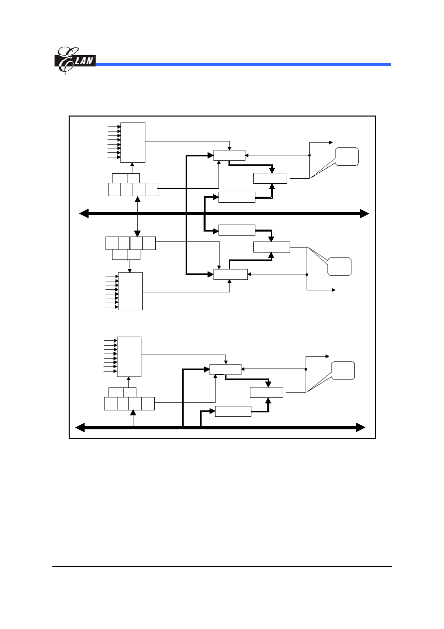
EM78P417N/418N/419N
8-Bit Microprocessor with OTP ROM
Product Specification (V1.0) 06.23.2005
∑ 53
(This specification is subject to change without further notice)
6.9.2 Function Description
The following figure shows the TMRX block diagram followed by descriptions of its
signals and blocks:
Data Bus
Data Bus
PRD1
Comparator
TMR1X
Period
Match
PRD2
Comparator
TMR2X
Period
Match
To PWM1IF
To PWM2IF
reset
reset
*TMR1X = TMR1H + TMR1L;
*TMR2X = TMR2H + TMR2L;
MUX
T1P2 T1P1 T1P0 T1EN
1:4
1:8
1:32
1:64
1:2
1:16
1:128
1:256
Fosc
Fosc
T2P2 T2P1 T2P0 T2EN
MUX
1:4
1:8
1:32
1:64
1:2
1:16
1:128
1:256
Data Bus
Data Bus
PRD3
Comparator
TMR3X
Period
Match
To PWM13F
reset
MUX
T3P2 T3P1 T3P0 T3EN
1:4
1:8
1:32
1:64
1:2
1:16
1:128
1:256
Fosc
*TMR3X = TMR3H + TMR3L
Fig. 6-12 TMRX Block Diagram
Fosc: Input clock.
Prescaler (T1P2, T1P1 and T1P0 / T2P2, T2P1 and T2P0 / T3P2, T3P1 and T3P0):
The options 1:2, 1:4, 1:8, 1:16, 1:32, 1:64, 1:128, and 1:256 are defined by
TMRX. It is cleared when any type of reset occurs.
TMR1X, TMR2X and TMR3X (TMR1H/TWR1L, TMR2H/TMR2L, & TMR3H/TMR3L):
Timer X register; TMRX is increased until it matches with PRDX, and then is
reset to 1 (default valve).

EM78P417N/418N/419N
8-Bit Microprocessor with OTP ROM
54
∑
Product Specification (V1.0) 06.23.2005
(This specification is subject to change without further notice)
PRDX (PRD1, PRD2 and PRD3):
PWM time period register.
ComparatorX (Comparator 1 and Comparator 2):
Reset TMRX while a match occurs. The TMRXIF flag is set at the same time.
6.9.3 Programming the Related Registers
When defining TMRX, refer to the related registers of its operation as shown in the
table below. It must be noted that the PWMX bits must be disabled if their related
TMRXs are employed. That is, Bit 7 ~ Bit 5 of the PWMCON register must be set to `0'.
6.9.3.1 Related Control Registers of TMR1, TMR2, and TMR3
Address
Name
Bit 7
Bit 6
Bit 5
Bit 4
Bit 3
Bit 2 Bit 1
Bit 0
IOC80 PWMCON/IOC80
PWM3E PWM2E PWM1E
"0" T1EN
T1P2 T1P1 T1P0
IOC90 TMRCON/IOC90 T3EN
T2EN
T3P2
T3P1
T3P0
T2P2 T2P1 T2P0
6.9.4 Timer Programming Process/Steps
1. Load PRDX with the TIMER duration
2. Enable interrupt function by writing IOCF0, if required
3. Load a desired a TMRX prescaler value to PWMCON and TMRCON and enable
TMRX and disable PWMX
6.10 Comparator
EM78P418/9N has one comparator comprising of two analog inputs and one output.
The comparator can be utilized to wake up EM78P418/9N from sleep mode. The
comparator circuit diagram is depicted in the figure below.
Cin -
-
+
CMP
Cin+
CO
Cin+
Cin-
Output
30mV
Fig. 6-13 Comparator Circuit Diagram & Operating Mode

EM78P417N/418N/419N
8-Bit Microprocessor with OTP ROM
Product Specification (V1.0) 06.23.2005
∑ 55
(This specification is subject to change without further notice)
6.10.1 External Reference Signal
The analog signal that is presented at Cin≠ compares to the signal at Cin+, and the
digital output (CO) of the comparator is adjusted accordingly by taking the following
notes into considerations:
NOTE
The reference signal must be between Vss and Vdd.
The reference voltage can be applied to either pin of comparator.
Threshold detector applications may be of the same reference.
The comparator can operate from the same or different reference sources.
6.10.2 Comparator
Outputs
The compared result is stored in the CMPOUT of IOCA0.
The comparator outputs are sent to CO(P60) through programming Bit 1,
Bit 0<COS1, COS0> of the IOCA0 register to <1,0>. See Section 6.2.6, IOCA0
(CMPCON: Comparator Control Register) for Comparator/OP select bits function
description.
NOTE
The CO and ADEO of the P60/ADE0/CO pins cannot be used at the same time.
The P60/ADE0/CO pin priority is as follows:
P60/ADE0/CO PRIORITY
High
Medium
Low
CO ADE0 P60
The following figure shows the Comparator Output block diagram.
Q
Q
EN
EN
D
D
To C0
To CPIF
To CMPOUT
CMRD
CMRD
From other
comparator
RESET
From OP I/O
Fig. 6-14 Comparator Output Configuration

EM78P417N/418N/419N
8-Bit Microprocessor with OTP ROM
56
∑
Product Specification (V1.0) 06.23.2005
(This specification is subject to change without further notice)
6.10.3 Using Comparator as an Operation Amplifier
The comparator can be used as an operation amplifier if a feedback resistor is
connected from the input to the output externally. In this case, the Schmitt trigger can
be disabled for power saving by setting Bit 1, Bit 0<COS1, COS0> of the IOCA0
register to <1,1>. See Section 6.2.6, IOCA0 (CMPCON: Comparator Control Register)
for Comparator/OP select bits function description.
6.10.4 Comparator
Interrupt
CMPIE (IOCF0.7) must be enabled for the "ENI" instruction to take effect
Interrupt is triggered whenever a change occurs on the comparator output pin
The actual change on the pin can be determined by reading the Bit CMPOUT,
IOCA0<2>
CMPIF (RF.7), the comparator interrupt flag, can only be cleared by software
6.10.5 Wake-up from SLEEP Mode
If enabled, the comparator remains active and the interrupt remains functional, even
under SLEEP mode.
If a mismatch occurs, the interrupt will wake up the device from SLEEP mode.
The power consumption should be taken into consideration for the benefit of energy
conservation.
If the function is unemployed during SLEEP mode, turn off comparator before
entering into sleep mode.
6.11 Oscillator
6.11.1 Oscillator
Modes
The EM78P417/8/9N can be operated in four different oscillator modes, such as High
XTAL oscillator mode (HXT), Low XTAL oscillator mode (LXT), External RC oscillator
mode (ERC), and RC oscillator mode with Internal RC oscillator mode (IRC). You can
select one of them by programming the OSC2, OCS1, and OSC0 in the CODE Option
register.
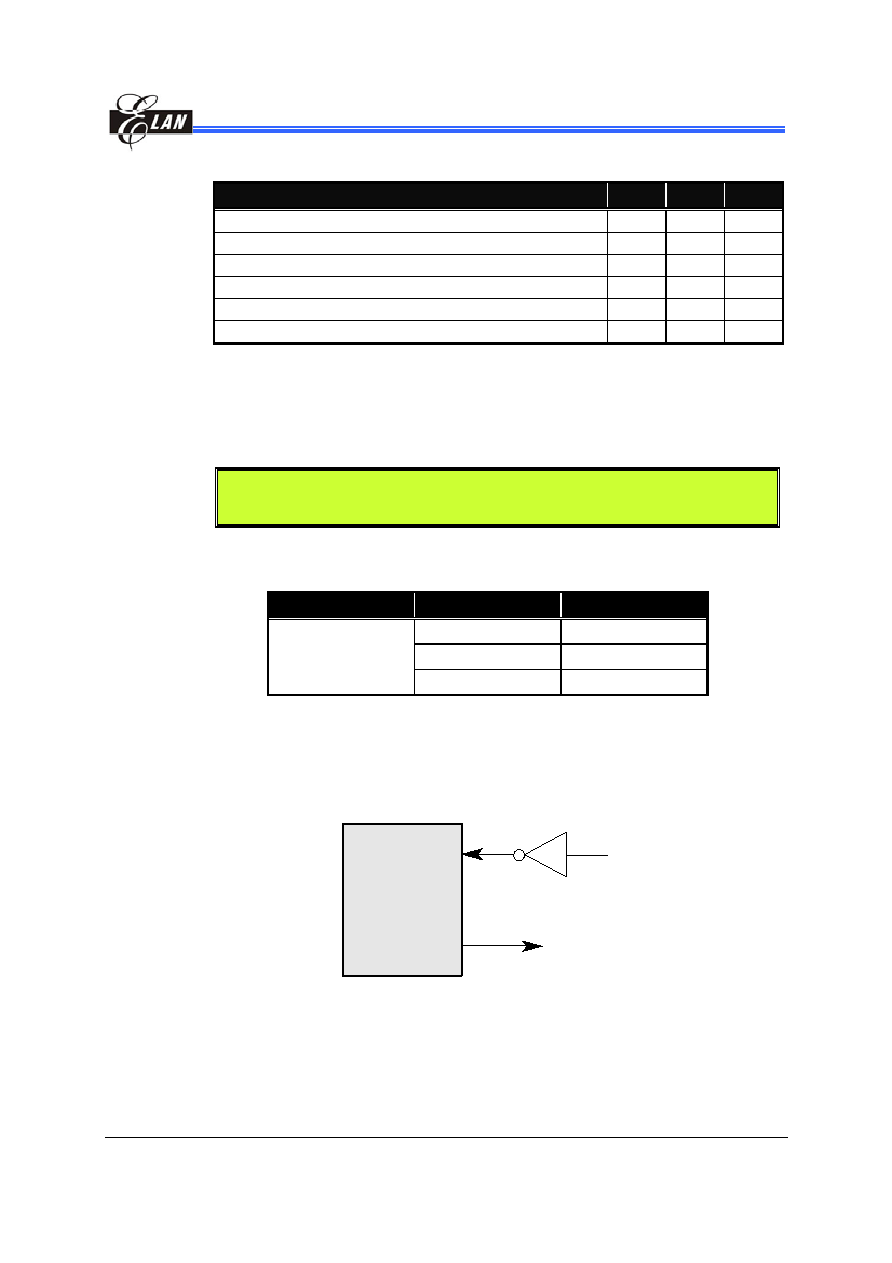
EM78P417N/418N/419N
8-Bit Microprocessor with OTP ROM
Product Specification (V1.0) 06.23.2005
∑ 57
(This specification is subject to change without further notice)
The Oscillator modes defined by OSC2, OCS1, and OSC0 are described below.
Oscillator Modes
OSC2 OSC1 OSC0
ERC
1
(External RC oscillator mode); P54/OSCO acts as P54
0
0
0
ERC
1
(External RC oscillator mode); P54/OSCO acts as OSCO
0
0
1
IRC
2
(Internal RC oscillator mode); P54/OSCO acts as P54
0
1
0
IRC
2
(Internal RC oscillator mode); P54/OSCO acts as OSCO
0
1
1
LXT
3
(Low XTAL oscillator mode)
1
1
0
HXT
3
High XTAL oscillator mode) (default)
1
1
1
1
Under ERC mode, OSCI is used as oscillator pin. OSCO/P54 is defined by code
option WORD0 Bit6 ~ Bit4.
2
Under IRC mode, P55 is normal I/O pin. OSCO/P54 is defined by code
option WORD0 Bit6 ~ Bit4.
3
Under LXT and HXT modes; OSCI and OSCO are used as oscillator pins. These
pins cannot and should not be defined as normal I/O pins.
NOTE
The transient point of the system frequency between HXT and LXY is around 400kHz.
The maximum operating frequency limit of crystal/resonator at different VDDs, are as
follows:
Conditions
VDD
Max. Freq. (MHz)
2.3 4
3.0 8
Two clocks
5.0 20
6.11.2 Crystal Oscillator/Ceramic Resonators (XTAL)
EM78P417/8/9N can be driven by an external clock signal through the OSCI pin as
illustrated below.
OSCI
OSCO
Ext.
Clock
EM78P417/ 8/ 9N
Fig. 6.15 External Clock Input Circuit
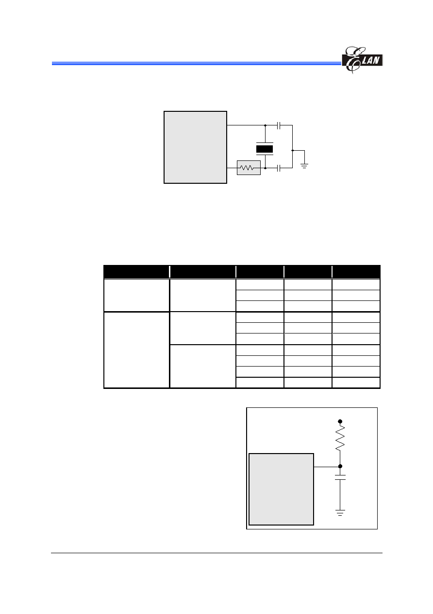
EM78P417N/418N/419N
8-Bit Microprocessor with OTP ROM
58
∑
Product Specification (V1.0) 06.23.2005
(This specification is subject to change without further notice)
In the most applications, Pin OSCI and Pin OSCO can be connected with a crystal or
ceramic resonator to generate oscillation. Fig. 6-16 below depicts such circuit. The
same applies to the HXT mode and the LXT mode.
OSCI
OSCO
C1
C2
XTAL
RS
EM78P417/ 8/ 9N
Fig. 6-16 Crystal/Resonator Circuit
The following table provides the recommended values for C1 and C2. Since each
resonator has its own attribute, you should refer to the resonator specifications for
appropriate values of C1 and C2. RS, a serial resistor, may be required for AT strip cut
crystal or low frequency mode.
Capacitor selection guide for crystal oscillator or ceramic resonators:
Oscillator Type
Frequency Mode
Frequency
C1(pF)
C2(pF)
455 kHz
100~150
100~150
2.0 MHz
20~40
20~40
Ceramic Resonators
HXT
4.0 MHz
10~30
10~30
32.768kHz
25
15
100KHz
25
25
LXT
200KHz
25
25
455KHz 20~40 20~150
1.0MHz 15~30 15~30
2.0MHz 15
15
Crystal Oscillator
HXT
4.0MHz 15
15
6.11.3 External RC Oscillator Mode
For some applications that do not require
precise timing calculation, the RC
oscillator (Fig. 6-17 right) could offer you
with effective cost savings. Nevertheless,
it should be noted that the frequency of
the RC oscillator is influenced by the
supply voltage, the values of the resistor
(Rext), the capacitor (Cext), and even by
the operation temperature. Moreover, the
frequency also changes slightly from one
chip to another due to the manufacturing
process variation.
OSCI
Vcc
Rext
Cext
EM78P417/ 8/ 9N
Fig. 6-17 External RC Oscillator Mode Circuit
EM78P417N/418N/419N
8-Bit Microprocessor with OTP ROM
Product Specification (V1.0) 06.23.2005
∑ 59
(This specification is subject to change without further notice)
In order to maintain a stable system frequency, the values of the Cext should be no less
than 20pF, and that the value of Rext should be no greater than 1M
. If the frequency
cannot be kept within this range, the frequency can be affected easily by noise,
humidity, and leakage.
The smaller the Rext in the RC oscillator is, the faster its frequency will be. On the
contrary, for very low Rext values, for instance, 1 K
, the oscillator will become
unstable because the NMOS cannot discharge the capacitance current correctly.
Based on the above reasons, it must be kept in mind that all supply voltage, the
operation temperature, the components of the RC oscillator, the package types, and
the way the PCB is layout, have certain effect on the system frequency.
The RC Oscillator frequencies:
Cext
Rext
Average Fosc 5V,25
∞C
Average Fosc 3V,25
∞C
3.3k
3.5 MHz
3.2 MHz
5.1k
2.5 MHz
2.3 MHz
10k
1.30 MHz
1.25 MHz
20 pF
100k
140 KHz
140 KHz
3.3k
1.27 MHz
1.21 MHz
5.1k
850 KHz
820 KHz
10k
450 KHz
450 KHz
100 pF
100k
48 KHz
50 KHz
3.3k
560 KHz
540 KHz
5.1k
370 KHz
360 KHz
10k
196 KHz
192 KHz
300 pF
100k
20 KHz
20 KHz
NOTE: 1. Measured on DIP packages.
2. Design reference only
3. The frequency drift is about ±30%
6.11.4 Internal RC Oscillator Mode
EM78P417/8/9N offers a versatile internal RC mode with default frequency value of
4MHz. Internal RC oscillator mode has other frequencies (1MHz, 8MHz, and 455KHz)
that can be set by CODE OPTION (WORD1), RCM1, and RCM0. Table below
describes the EM78P417/8/9N internal RC drift with the variation of voltage,
temperature, and process.
EM78P417N/418N/419N
8-Bit Microprocessor with OTP ROM
60
∑
Product Specification (V1.0) 06.23.2005
(This specification is subject to change without further notice)
Internal RC Drift Rate (Ta=25, VDD=5V±5%, VSS=0V)
Drift Rate
Internal
RC Frequency
Temperature
(-40~+80)
Voltage
(2.3V~5.5V)
Process
Total
4MHz ±10%
±5%
±4% ±19%
8MHz ±10%
±6%
±4% ±20%
1MHz ±10%
±5%
±4% ±19%
455MHz ±10%
±5%
±4%
±19%
Theoretical values are for reference only. Actual values may vary depending on actual process.
6.12 Power-on Considerations
Any microcontroller is not warranted to start operating properly before the power supply
stabilizes in steady state. EM78P417/8/9N is equipped with Power On Voltage
Detector (POVD) with detection level range of 1.9V to 2.1V. The circuitry eliminates the
extra external reset circuit. It will work well if Vdd rises quickly enough (50 ms or less).
However, under critical applications, extra devices are still required to assist in solving
power-on problems.
6.12.1 External Power-on Reset Circuit
The circuit shown in the
following figure implements
an external RC to produce a
reset pulse. The pulse
width (time constant) should
be kept long enough to
allow Vdd to reach the
minimum operating voltage.
This circuit is used when the
power supply has a slow
power rise time. Because
EM78P417/ 8/ 9N
/RESET
VDD
D
R
Rin
C
Fig. 6-18 External Power on Reset Circuit
the current leakage from the /RESET pin is about
±5µA, it is recommended that R
should not be great than 40 K. This way, the voltage at Pin /RESET is held below 0.2V.
The diode (D) acts as a short circuit at power-down. The "C" capacitor is discharged
rapidly and fully. Rin, the current-limited resistor, prevents high current discharge or
ESD (electrostatic discharge) from flowing into Pin /RESET.
EM78P417N/418N/419N
8-Bit Microprocessor with OTP ROM
Product Specification (V1.0) 06.23.2005
∑ 61
(This specification is subject to change without further notice)
6.12.2 Residual Voltage Protection
When the battery is replaced, device power (Vdd) is removed but residual voltage
remains. The residual voltage may trips below Vdd minimum, but not to zero. This
condition may cause a poor power on reset. Fig. 6-16 and Fig. 6-20 show how to
create a protection circuit against residual voltage.
EM78P417/ 8/ 9N
/RESET
VDD
100K
Q1
1N4684
10K
33K
VDD
Fig. 6-19 Residual Voltage Protection Circuit 1
EM78P417/ 8/ 9N
/RESET
VDD
Q1
VDD
R3
R2
R1
Fig. 6-20 Residual Voltage Protection Circuit 2
6.13 Code Option
EM78P417/8/9N has two CODE option words and one Customer ID word that are not a
part of the normal program memory.
Word 0
Word1
Word 2
Bit12 ~ Bit0
Bit12 ~ Bit0
Bit12 ~ Bit0
EM78P417N/418N/419N
8-Bit Microprocessor with OTP ROM
62
∑
Product Specification (V1.0) 06.23.2005
(This specification is subject to change without further notice)
6.13.1 Code Option Register (Word 0)
WORD 0
Bit 12 Bit 11 Bit 10 Bit 9 Bit 8 Bit 7
Bit 6
Bit 5
Bit 4
Bit 3
Bit 2 Bit 1 Bit 0
≠ ≠ ≠
TYPE
CLKS
ENWDTB
OSC2
OSC1
OSC0
HLP
PR2 PR1 PR0
Bit 12 ~ 10:
Not used (reserved). These bits are set to "1" all the time
Bit 9 (TYPE):
Type selection for EM78P419N or EM78P418N or EM78P417N.
0 = EM78P419N
1 = EM78P417N/EM78P418N (default)
Bit 8 (CLKS):
Instruction time period option bit
0 = two oscillator time periods
1 = four oscillator time periods (default)
Refer to the Section 6.15 for Instruction Set
Bit 7 (ENWDTB): Watchdog timer enable bit
0 = Enable
1 = Disable (default)
Bit 6, 5 & 4 (OSC2, OSC1 & OSC0): Oscillator Modes Selection bits
Oscillator Modes
OSC2 OSC1 OSC0
ERC
1
(External RC oscillator mode); P54/OSCO acts as P54
0
0
0
ERC
1
(External RC oscillator mode); P54/OSCO acts as OSCO
0
0
1
IRC
2
(Internal RC oscillator mode); P54/OSCO acts as P54
0
1
0
IRC
2
(Internal RC oscillator mode); P54/OSCO acts as OSCO
0
1
1
LXT
3
(Low XTAL oscillator mode)
1
1
0
HXT
3
High XTAL oscillator mode) (default)
1
1
1
1
Under ERC mode, OSCI is used as oscillator pin. OSCO/P54 is defined by code
option WORD0 Bit6 ~ Bit4.
2
Under IRC mode, P55 is normal I/O pin. OSCO/P54 is defined by code
option WORD0 Bit6 ~ Bit4.
3
Under LXT and HXT modes; OSCI and OSCO are used as oscillator pins. These
pins cannot and should not be defined as normal I/O pins.
NOTE
The transient point of the system frequency between HXT and LXY is around 400kHz.
Bit 3 (HLP):
Power consumption selection
0 = Low power consumption, applies to working frequency
at 4MHz or below 4MHz
1 = High power consumption, applies to working frequency
above 4MHz
EM78P417N/418N/419N
8-Bit Microprocessor with OTP ROM
Product Specification (V1.0) 06.23.2005
∑ 63
(This specification is subject to change without further notice)
Bit 2 ~ 0 (PR2 ~ PR0):
Protect Bit
PR2 ~ PR0 are protect bits. Each protect status is as
follows:
PR2
PR1
PR0
Protect
0 0 0 Enable
0 0 1 Enable
0 1 0 Enable
0 1 1 Enable
1 0 0 Enable
1 0 1 Enable
1 1 0 Enable
1 1 1 Disable
6.13.2 Code Option Register (Word 1)
WORD 1
Bit 12 Bit 11 Bit 10 Bit 9 Bit 8 Bit 7
Bit 6
Bit 5
Bit 4
Bit 3
Bit 2 Bit 1 Bit 0
≠ ≠ ≠ ≠
NRHL
NRE
CYES
C3
C2
C1
C0
RCM1
RCM0
Bits 12 ~ 9:
Not used (reserved). These bits are set to "1" all the time
Bit 8 (NRHL):
Noise rejection high/low pulses define bit. INT pin is falling edge
trigger
0 = Pulses equal to 8/fc [s] is regarded as signal.
1 = Pulses equal to 32/fc [s] is regarded as signal.
(default)
NOTE
The noise rejection function is turned off under the LXT and sleep mode.
Bit 7 (NRE):
Noise rejection enable
0 = disable noise rejection
1 = enable noise rejection (default). However under Low XTAL
oscillator (LXT) mode, the noise rejection circuit always
disabled.
Bit 6 (CYES):
Instruction cycle selection bit
0 = one instruction cycle
1 = two instruction cycles (default)
Bits 5, 4, 3 & Bit2 ( C3, C2, C1, & C0 ): Calibrator of internal RC mode. These bits
must always be set to "1" only (auto calibration)

EM78P417N/418N/419N
8-Bit Microprocessor with OTP ROM
64
∑
Product Specification (V1.0) 06.23.2005
(This specification is subject to change without further notice)
Bit 1 & Bit 0 (RCM1 & RCM0): RC mode selection bits
RCM 1
RCM 0
Frequency(MHz)
1 1
4
1 0
8
0 1
1
0 0
455kHz
6.13.3 Customer ID Register (Word 2)
WORD 2
Bit 12 Bit 11 Bit 10 Bit 9 Bit 8 Bit 7
Bit 6
Bit 5
Bit 4
Bit 3
Bit 2 Bit 1 Bit 0
X X X X X X X X X X X X X
Bit 12 ~ 0 : Customer's ID code
6.14 Instruction Set
Each instruction in the instruction set is a 13-bit word divided into an OP code and one
or more operands. Normally, all instructions are executed within one single instruction
cycle (one instruction consists of 2 oscillator time periods), unless the program counter
is changed by instructions "MOV R2,A," "ADD R2,A," or by instructions of arithmetic or
logic operation on R2 (e.g., "SUB R2,A," "BS(C) R2,6," "CLR R2," etc.). In this case,
these instructions need one or two instruction cycles as determined by Code Option
Register CYES bit.
In addition, the instruction set has the following features:
1. Every bit of any register can be set, cleared, or tested directly.
2. The I/O registers can be regarded as general registers. That is, the same
instruction can operate on I/O registers.
The symbol "R" represents a register designator that specifies which one of the
registers (including operational registers and general-purpose registers) is to be
utilized by the instruction. The symbol "b" represents a bit field designator that selects
the value for the bit located in the register "R" that is affected by the operation. The
symbol "k" represents an 8 or 10-bit constant or literal value.

EM78P417N/418N/419N
8-Bit Microprocessor with OTP ROM
Product Specification (V1.0) 06.23.2005
∑ 65
(This specification is subject to change without further notice)
The following are the list of the EM78P417/8/9N instruction set
Instruction Binary HEX Mnemonic
Operation
Status Affected
0 0000 0000 0000
0000 NOP
No Operation
None
0 0000 0000 0001
0001 DAA
Decimal Adjust A
C
0 0000 0000 0010
0002 CONTW
A
CONT
None
0 0000 0000 0011
0003 SLEP
0
WDT, Stop oscillator
T,P
0 0000 0000 0100
0004 WDTC
0
WDT
T,P
0 0000 0000 rrrr
000r IOW R
A
IOCR
None
1
0 0000 0001 0000
0010 ENI
Enable Interrupt
None
0 0000 0001 0001
0011 DISI
Disable Interrupt
None
0 0000 0001 0010
0012 RET
[Top of Stack]
PC
None
0 0000 0001 0011
0013 RETI
[Top of Stack]
PC, Enable Interrupt
None
0 0000 0001 0100
0014 CONTR
CONT
A
None
0 0000 0001 rrrr
001r IOR R
IOCR
A
None
1
0 0000 01rr rrrr
00rr
MOV R,A
A
R
None
0 0000 1000 0000
0080 CLRA
0
A
Z
0 0000 11rr rrrr
00rr
CLR R
0
R
Z
0 0001 00rr rrrr
01rr
SUB A,R
R-A
A
Z,C,DC
0 0001 01rr rrrr
01rr
SUB R,A
R-A
R
Z,C,DC
0 0001 10rr rrrr
01rr
DECA R
R-1
A
Z
0 0001 11rr rrrr
01rr
DEC R
R-1
R
Z
0 0010 00rr rrrr
02rr
OR A,R
A
VR A
Z
0 0010 01rr rrrr
02rr
OR R,A
A
VR R
Z
0 0010 10rr rrrr
02rr
AND A,R
A & R
A
Z
0 0010 11rr rrrr
02rr
AND R,A
A & R
R
Z
0 0011 00rr rrrr
03rr
XOR A,R
A
R A
Z
0 0011 01rr rrrr
03rr
XOR R,A
A
R R
Z
0 0011 10rr rrrr
03rr
ADD A,R
A + R
A
Z,C,DC
0 0011 11rr rrrr
03rr
ADD R,A
A + R
R
Z,C,DC
0 0100 00rr rrrr
04rr
MOV A,R
R
A
Z
0 0100 01rr rrrr
04rr
MOV R,R
R
R
Z
0 0100 10rr rrrr
04rr
COMA R
/R
A
Z
0 0100 11rr rrrr
04rr
COM R
/R
R
Z
0 0101 00rr rrrr
05rr
INCA R
R+1
A
Z
0 0101 01rr rrrr
05rr
INC R
R+1
R
Z
0 0101 10rr rrrr
05rr
DJZA R
R-1
A, skip if zero
None
0 0101 11rr rrrr
05rr
DJZ R
R-1
R, skip if zero
None
0 0110 00rr rrrr
06rr
RRCA R
R(n)
A(n-1),R(0) C, C A(7)
C
0 0110 01rr rrrr
06rr
RRC R
R(n)
R(n-1),R(0) C, C R(7)
C
0 0110 10rr rrrr
06rr
RLCA R
R(n)
A(n+1),R(7) C, C A(0)
C
0 0110 11rr rrrr
06rr
RLC R
R(n)
R(n+1),R(7) C, C R(0)
C
0 0111 00rr rrrr
07rr
SWAPA R
R(0-3)
A(4-7),R(4-7) A(0-3)
None
0 0111 01rr rrrr
07rr
SWAP R
R(0-3)
R(4-7)
None
0 0111 10rr rrrr
07rr
JZA R
R+1
A, skip if zero
None
0 0111 11rr rrrr
07rr
JZ R
R+1
R, skip if zero
None
0 100b bbrr rrrr
0xxx BC R,b
0
R(b)
None
2
0 101b bbrr rrrr
0xxx BS R,b
1
R(b)
None
3
0 110b bbrr rrrr
0xxx JBC R,b
if R(b)=0, skip
None
0 111b bbrr rrrr
0xxx JBS R,b
if R(b)=1, skip
None
1 00kk kkkk kkkk
1kkk CALL k
PC+1
[SP],(Page, k) PC
None

EM78P417N/418N/419N
8-Bit Microprocessor with OTP ROM
66
∑
Product Specification (V1.0) 06.23.2005
(This specification is subject to change without further notice)
Instruction Binary HEX Mnemonic
Operation
Status Affected
1 01kk kkkk kkkk
1kkk JMP k
(Page, k)
PC
None
1 1000 kkkk kkkk
18kk MOV A,k
k
A
None
1 1001 kkkk kkkk
19kk OR A,k
A
k A
Z
1 1010 kkkk kkkk
1Akk AND A,k
A & k
A
Z
1 1011 kkkk kkkk
1Bkk XOR A,k
A
k A
Z
1 1100 kkkk kkkk
1Ckk RETL k
k
A,[Top of Stack] PC
None
1 1101 kkkk kkkk
1Dkk SUB A,k
k-A
A
Z,C,DC
1 1111 kkkk kkkk
1Fkk ADD A,k
k+A
A
Z,C,DC
1
This instruction is applicable to IOC50 ~ IOCF0, IOC51 ~ IOCF1 only.
2
This instruction is not recommended for RF operation.
3
This instruction cannot operate under RF.
7 Absolute Maximum Ratings
Items
Rating
Temperature under bias
-40
∞C to
85
∞C
Storage temperature
-65
∞C to
150
∞C
Input voltage
Vss-0.3V to
Vdd+0.5V
Output voltage
Vss-0.3V
to
Vdd+0.5V
Working Voltage
2.5V
to
5.5V
Working Frequency
DC
to
20MHz

EM78P417N/418N/419N
8-Bit Microprocessor with OTP ROM
Product Specification (V1.0) 06.23.2005
∑ 67
(This specification is subject to change without further notice)
8 DC Electrical Characteristics
(Ta= 25
∞C, VDD= 5.0V, VSS= 0V )
Symbol
Parameter
Condition
Min.
Typ.
Max.
Unit
XTAL: VDD to 5V
DC
20
MHz
XTAL: VDD to 3V
Two cycle with two clocks
DC
8 MHz
FXT
ERC: VDD to 5V
R: 5.1K
, C: 100 pF
F
±30% 850
F
±30% KHz
IRC1 IRC:VDD to 5V
RCM0:RCM1=1:1 3.84
4.0
4.16
MHz
IRC2 IRC:VDD to 5V
RCM0:RCM1=1:0 7.68
8.0
8.32
MHz
IRC3 IRC:VDD to 5V
RCM0:RCM1=0:1 0.96
1.0
1.06
MHz
IRC4 IRC:VDD to 5V
RCM0:RCM1=0:0 436.8
455
473.2
KHz
VIHRC
Input High Threshold
Voltage (Schmitt trigger )
OSCI in RC mode
3.5
V
VILRC
Input Low Threshold Voltage
(Schmitt trigger )
OSCI in RC mode
1.5
V
IIL
Input Leakage Current for
input pins
VIN = VDD, VSS
≠1.0
0
1.0
µA
VIH1
Input High Voltage (Schmitt
trigger )
Ports 5, 6, 7
3.75
V
VIL1
Input Low Voltage (Schmitt
trigger )
Ports 5, 6, 7
1.25
V
VIHT1
Input High Threshold
Voltage (Schmitt trigger )
/RESET
2.0
V
VILT1
Input Low Threshold Voltage
(Schmitt trigger )
/RESET
1.0
V
VIHT2
Input High Threshold
Voltage (Schmitt trigger )
TCC,INT
3.75
V
VILT2
Input Low Threshold Voltage
(Schmitt trigger )
TCC,INT
1.25
V
VIHX1 Clock Input High Voltage
OSCI in crystal mode
3.5
V
VILX1 Clock Input Low Voltage
OSCI in crystal mode
1.5
V
IOH1
Output High Voltage
(Ports 5, 6, 7)
VOH = VDD-0.5V (IOH =-6mA)
-6.0
mA
IOL1
Output Low Voltage
(Ports 5, 6,7)
VOL = GND+0.5V (IOL =12mA)
12.0
mA
IPH Pull-high current
Pull-high active, input pin at VSS ≠50
≠75
≠240
µA
IPL
Pull-low current
Pull-low active, input pin at Vdd
25
40
120
µA
ISB1
Power down current
All input and I/O pins at VDD,
output pin floating, WDT disabled
1.0
2.0
µA
ISB2
Power down current
All input and I/O pins at VDD,
output pin floating, WDT enabled
15
µA
ICC1
Operating supply current
at two clocks
/RESET= 'High', Fosc=32KHz
(Crystal type,CLKS="0"), output
pin floating, WDT disabled
15 20 35
µA
ICC2
Operating supply current
at two clocks
/RESET= 'High', Fosc=32KHz
(Crystal type,CLKS="0"), output
pin floating, WDT enabled
25 35
µA
ICC3
Operating supply current
at two clocks
/RESET= 'High', Fosc=4MHz
(Crystal type, CLKS="0"), output
pin floating, WDT enabled
1.7
2.2
mA
ICC4
Operating supply current
at two clocks
/RESET= 'High', Fosc=10MHz
(Crystal type, CLKS="0"), output
pin floating, WDT enabled
3.0
3.5
mA

EM78P417N/418N/419N
8-Bit Microprocessor with OTP ROM
68
∑
Product Specification (V1.0) 06.23.2005
(This specification is subject to change without further notice)
8.1 AD Converter Characteristic
(Vdd=2.5V to 5.5V,Vss=0V,Ta=25)
Symbol
Parameter
Condition
Min.
Typ.
Max.
Unit
V
AREF
2.5 Vdd
V
V
ASS
Analog reference voltage
V
AREF
- V
ASS
2.5V
Vss
Vss
V
VAI
Analog input voltage
V
V
ASS
AREF
V
Ivdd 750
850
1000
uA
IAI1
Ivref
Analog supply current
Vdd=V
AREF
=5.0V, V
ASS
=0.0V(V reference from Vdd)
-10 0 +10
uA
Ivdd 500
600
820
uA
IAI2
IVref
Analog supply current
Vdd=V
AREF
=5.0V, V
ASS
=0.0V(V reference from
VREF)
200 250 300
uA
IOP OP
current
Vdd=5.0V, OP used
Output voltage swing 0.2V to
4.8V
450 550 650
uA
RN Resolution
Vdd=V
AREF
=5.0V, V
ASS
=0.0V
10
11
Bits
LN
Linearity error
Vdd = 2.5 to 5.5V Ta=25 0 ±4 ±8
LSB
DNL
Differential nonlinear error
Vdd = 2.5 to 5.5V Ta=25 0 ±0.5
±0.9
LSB
FSE
Full scale error
Vdd=V
AREF
=5.0V, V
ASS
=0.0V
±0
±4
±8
LSB
OE Offset
error
Vdd=V
AREF
=5.0V, V
ASS
=0.0V
±0
±2
±4
LSB
ZAI
Recommended impedance of
analog voltage source
0
8
10
K
TAD
ADC clock duration
Vdd=V
AREF
=5.0V, V
ASS
=0.0V
4
us
TCN
AD conversion time
Vdd=V
AREF
=5.0V, V
ASS
=0.0V
15
15
TAD
ADIV
ADC OP input voltage range
Vdd=V
AREF
=5.0V, V
ASS
=0.0V
0
V
AREF
V
0 0.2 0.3
ADOV
ADC OP output voltage swing
Vdd=V
AREF
=5.0V, V
ASS
=0.0V,RL=10K
4.7 4.8 5
V
ADSR
ADC OP slew rate
Vdd=V
AREF
=5.0V, V
ASS
=0.0V
0.1
0.3
V/us
PSR
Power Supply Rejection
Vdd=5.0V±0.5V
±0
±2
LSB
NOTE: 1. These parameters are hypothetical (not tested) and are provided for design reference only.
2. There is no current consumption when ADC is off other than minor leakage current.
3. AD conversion result will not decrease when the input voltage is increased, and no missing code
will result.
4. These parameters are subject to change without further notice.

EM78P417N/418N/419N
8-Bit Microprocessor with OTP ROM
Product Specification (V1.0) 06.23.2005
∑ 69
(This specification is subject to change without further notice)
8.2 Comparator (OP) Characteristic
(Vdd = 5.0V,Vss=0V,Ta=25)
Symbol
Parameter
Condition
Min.
Typ.
Max.
Unit
SR Slew
rate
0.1
0.2 V/us
IVR
Input voltage range
Vdd =5.0V, V
SS
=0.0V
0 5 V
0 0.2 0.3
OVS
Output voltage swing
Vd =5.0V, V
SS
=0.0V,RL=10K
4.7 4.8 5
V
Iop
Supply current of OP
250
350
500
uA
Ico
Supply current of Comparator
300
uA
PSRR
Power-supply Rejection Ration
for OP
Vdd= 5.0V, V
SS
=0.0V
50
60
70
dB
Vs Operating
range
2.5 5.5
V
NOTE: 1. These parameters are hypothetical (not tested) and are provided for design reference only.
2. These parameters are subject to change without further notice.
8.3 Device
Characteristics
The graphs below were derived based on a limited number of samples and they are
provided for reference only. Hence, the device characteristic shown herein cannot be
guaranteed as fully accurate. In these graphs, the data maybe out of the specified
operating warranted range.
IRC OSC Frequency (VDD=3V)
0
1
2
3
4
5
6
7
8
9
-40
-20
0
25
70
50
85
Temperature ()
Frequency (M Hz) .
Fig. 8-1 Internal RC OSC Frequency vs. Temperature, VDD=3V
EM78P417N/418N/419N
8-Bit Microprocessor with OTP ROM
70
∑
Product Specification (V1.0) 06.23.2005
(This specification is subject to change without further notice)
IRC OSC Frequency (VDD=5V)
0
5
6
c
y (
M
1
2
3
F
r
e
q
4
7
8
9
10
-2
0
50
70
85
Temp
e ()
u
e
n
H
z
)
.
-40
0
25
eratur
. 8-2 Inter
Frequency vs. Temperature, VDD=
9
E
aract
Fig
nal RC OSC
5V
AC lectrical Ch
eristic
(Ta=25
∞C, VDD=5V±5%, VSS=0V)
Symbol
Parameter
Conditions
Min
Type
Max
Unit
Dclk
Input CLK duty cycle
45
50
55
%
Crystal type
100
DC
ns
Tins
Instruction cycle time
(CLKS="0")
RC type
500
DC
ns
Ttcc
TCC input time period
(Tins+20)/N
*
ns
Tdrh
Device reset hold time
Ta = 25
∞C 11.3
16.2 21.6 ms
Trst
/RESET pulse width
Ta = 25
∞C 2000
ns
Twdt
Watchdog timer duration
Ta = 25
∞C 11.3
16.2 21.6 ms
Tset
Input pin setup time
0
ns
Thold
Input pin hold time
15
20
25
ns
Tdelay
Output pin delay time
Cload=20pF
45
50
55
ns
Tdrc
ERC delay time
Ta = 25
∞C 1
3
5 ns
*
N = selected prescaler ratio
EM78P417N/418N/419N
8-Bit Microprocessor with OTP ROM
Product Specification (V1.0) 06.23.2005
∑ 71
(This specification is subject to change without further notice)
10 Timing Diagrams
RESET Timing (CLK="0")
CLK
/RESET
NOP
Instruction 1
Executed
Tdrh
TCC Input Timing (CLKS="0")
CLK
TCC
Ttcc
Tins
AC Testing : Input is driven at VDD-0.5V for logic "1",and GND+0.5V for logic "0".Timing
measurements are made at 0.75VDD for logic "1",and 0.25VDD for logic "0".
AC Test Input/Output Waveform
VDD-0.5V
GND+0.5V
0.75VDD
0.25VDD
TEST POINTS
0.75VDD
0.25VDD
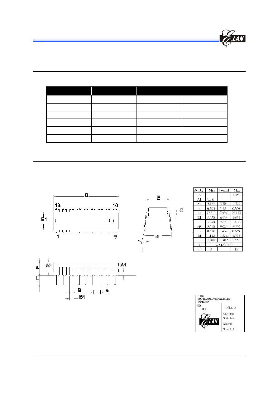
EM78P417N/418N/419N
8-Bit Microprocessor with OTP ROM
72
∑
Product Specification (V1.0) 06.23.2005
(This specification is subject to change without further notice)
APPENDIX
A Package
Types
OTP MCU
Package Type
Pin Count
Package Size
EM78P417NP DIP
18
pin
300mil
EM78P417NM SOP
18
pin
300mil
EM78P418NP DIP
20
pin
300mil
EM78P418NM SOP
20
pin
300mil
EM78P419NK
Skinny DIP
24 pin
300mil
EM78P419NM SOP
24
pin
300mil
B Packaging Configurations
B.1 18-Lead Plastic Dual in line (PDIP) -- 300 mil
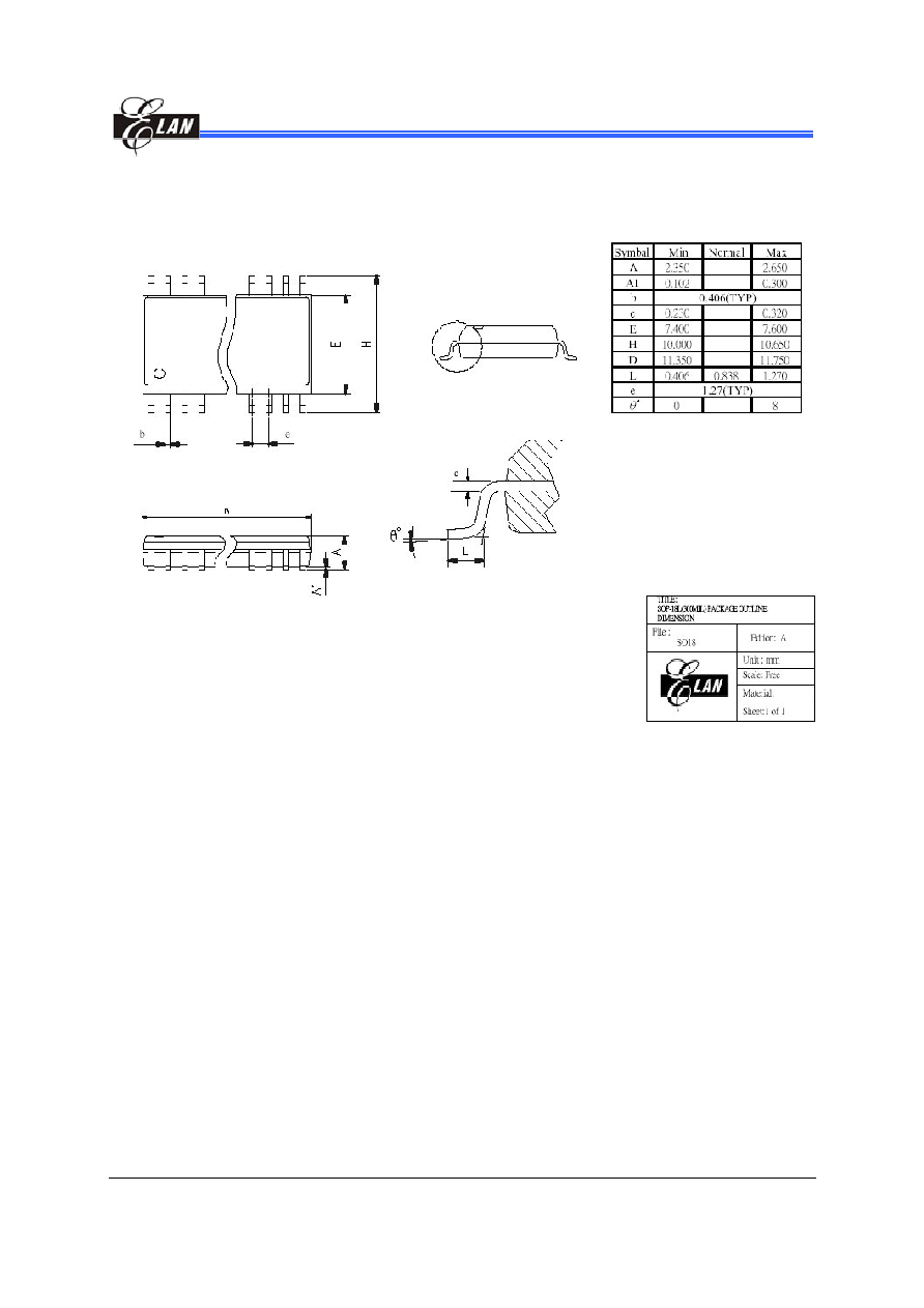
EM78P417N/418N/419N
8-Bit Microprocessor with OTP ROM
Product Specification (V1.0) 06.23.2005
∑ 73
(This specification is subject to change without further notice)
B.2 18-Lead Plastic Small Outline (SOP) -- 300 mil
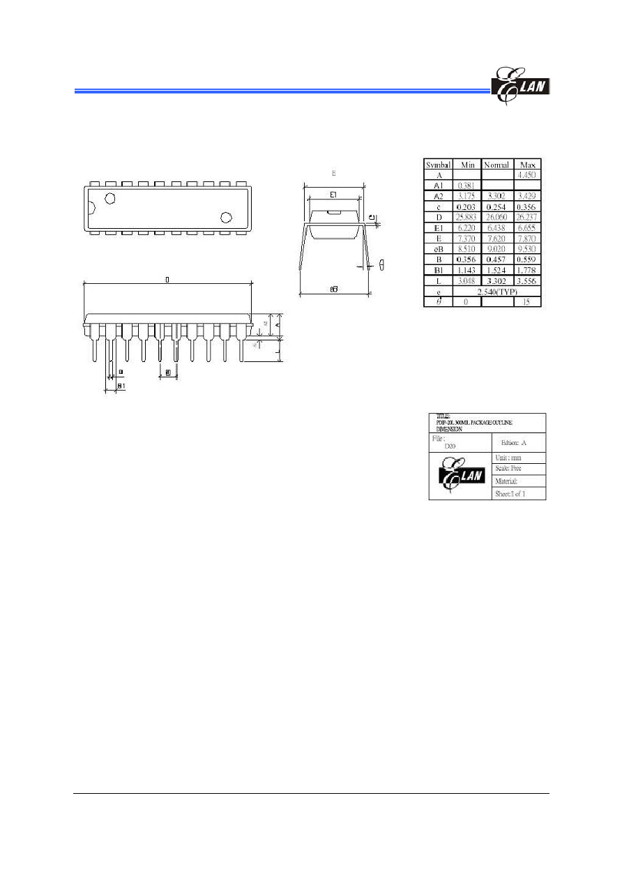
EM78P417N/418N/419N
8-Bit Microprocessor with OTP ROM
74
∑
Product Specification (V1.0) 06.23.2005
(This specification is subject to change without further notice)
B.3 20-Lead Plastic Dual in line (PDIP) -- 300 mil
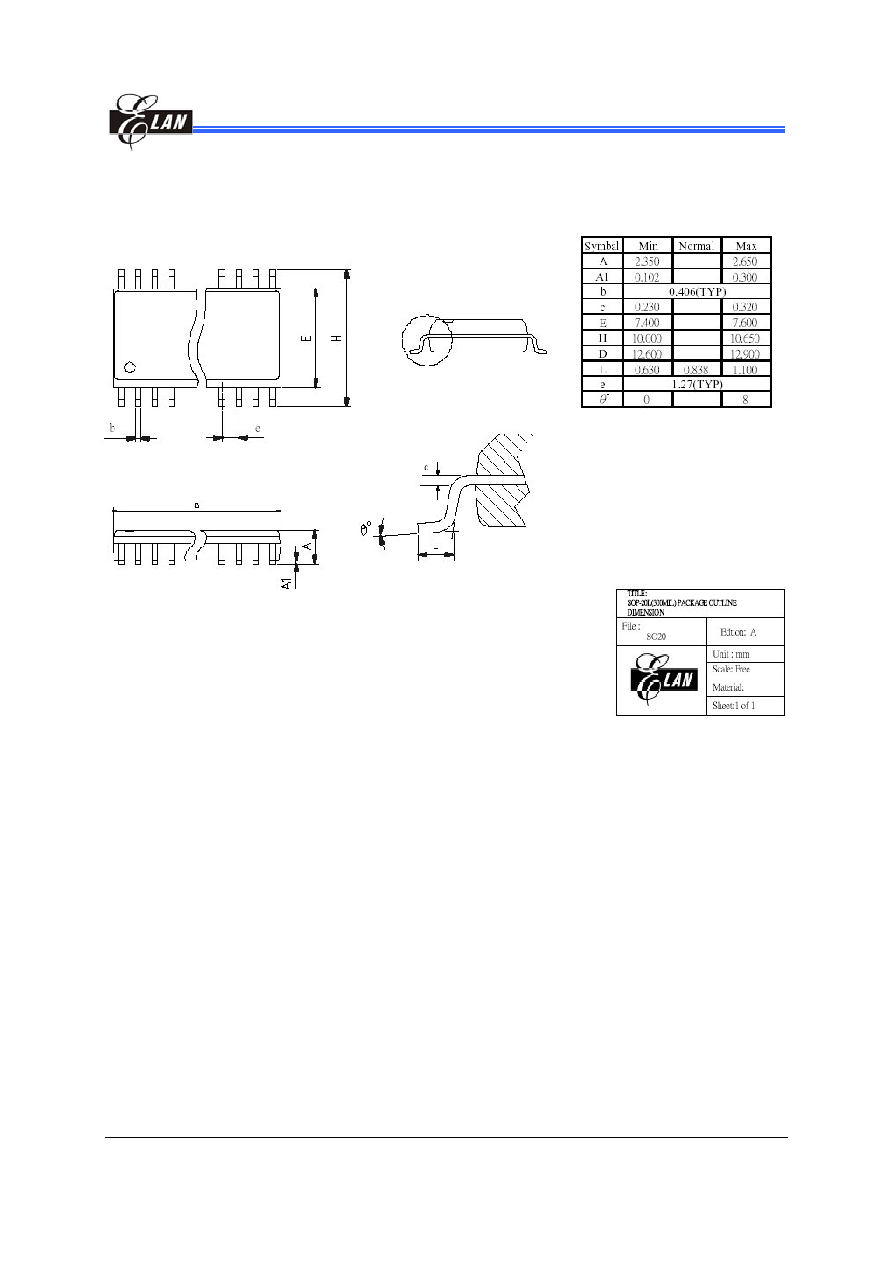
EM78P417N/418N/419N
8-Bit Microprocessor with OTP ROM
Product Specification (V1.0) 06.23.2005
∑ 75
(This specification is subject to change without further notice)
B.4 20-Lead Plastic Small Outline (SOP) -- 300 mil
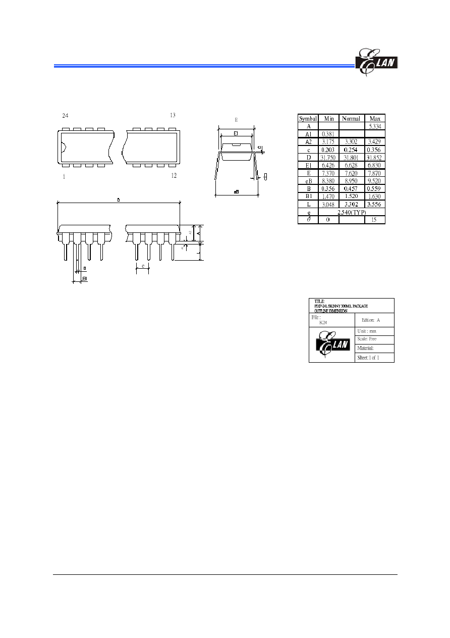
EM78P417N/418N/419N
8-Bit Microprocessor with OTP ROM
76
∑
Product Specification (V1.0) 06.23.2005
(This specification is subject to change without further notice)
B.5 24-Lead Plastic Dual in line (PDIP) -- 300 mil

EM78P417N/418N/419N
8-Bit Microprocessor with OTP ROM
Product Specification (V1.0) 06.23.2005
∑ 77
(This specification is subject to change without further notice)
B.6 24-Lead Plastic Small Outline (SOP) -- 300 mil

EM78P417N/418N/419N
8-Bit Microprocessor with OTP ROM
78
∑
Product Specification (V1.0) 06.23.2005
(This specification is subject to change without further notice)
C Quality Assurance and Reliability
Test Category
Test Conditions
Remarks
Solderability
Solder temperature=245
±5, for 5 seconds up to the
stopper using a rosin-type flux
Step 1: TCT, 65 (15mins)~150 (15mins), 10 cycles
Step 2: Bake at 125, TD (endurance)=24 hrs
Step 3: Soak at 30
∞C/60%TD (endurance)=192 hrs
Pre-condition
Step 4: IR flow 3 cycles
(Pkg
thickness2.5mm or
Pkg volume350mm3 ----225
±5)
(Pkg
thickness2.5mm or
Pkg volume350mm3 ----240
±5 )
For SMD IC (such as
SOP, QFP, SOJ, etc)
Temperature cycle test -65 (15mins)~150 (15mins), 200 cycles
Pressure cooker test
TA =121, RH=100%, pressure=2 atm,
TD (endurance)= 96 hrs
High temperature /
High humidity test
TA=85 , RH=85%TD (endurance)=168 , 500 hrs
High-temperature
storage life
TA=150, TD (endurance)=500, 1000 hrs
High-temperature
operating life
TA=125, VCC=Max. operating voltage,
TD (endurance) =168, 500, 1000 hrs
Latch-up TA=25, VCC=Max. operating voltage, 150mA/20V
ESD (HBM)
TA=25, ± 3KV
ESD (MM)
TA=25, ± 300V
IP_ND,OP_ND,IO_ND
IP_NS,OP_NS,IO_NS
IP_PD,OP_PD,IO_PD,
IP_PS,OP_PS,IO_PS,
VDD-VSS(+),VDD_VSS
(-)mode
C.1 Address Trap Detect
An address trap detect is one of the MCU embedded fail-safe functions that detects
MCU malfunction caused by noise or the like. Whenever the MCU attempts to fetch an
instruction from a certain section of ROM, an internal recovery circuit is auto started. If
a noise caused address error is detected, the MCU will repeat execution of the program
until the noise is eliminated. The MCU will then continue to execute the next program.