
EM78P468N
8-BIT
Microcontroller
Product
Specification
D
OC
.
V
ERSION
1.2
ELAN
MICROELECTRONICS
CORP.
March 2005

Trademark Acknowledgments:
IBM is a registered trademark and PS/2 is a trademark of IBM.
Windows is a trademark of Microsoft Corporation.
LAN and ELAN logo
are trademarks of ELAN Microelectronics Corporati
E
on.
LAN Microelectronics Corporation
rinted in Taiwan, ROC
contained in this specification.
irect, indirect, special incidental, or consequential damages arising out of the use of such information
e or nondisclosure agreement, and
ces, or systems. Use of
NY MEANS WITHOUT THE EXPRESS WRITTEN PERMISSION OF ELAN MICROELECTRONICS.
ELAN MICROELECTRONICS CORPORATION
. 30077
http://www.emc.com.tw
Copyright
� 2005 by E
All Rights Reserved
P
The contents of in this specification are subject to change without notice. ELAN Microelectronics assumes no
responsibility concerning the accuracy, adequacy, or completeness of this specification. ELAN Microelectronics
makes no commitment to update, or to keep current the information and material
Such information and material may change to conform to each confirmed order.
In no event shall ELAN Microelectronics be made responsible to any claims attributed to errors, omissions, or
other inaccuracies in the information or material contained in this specification. ELAN Microelectronics shall not
be liable for d
or material.
The software (if any) described in this specification is furnished under a licens
may be used or copied only in accordance with the terms of such agreement.
ELAN Microelectronics products are not intended for use in life support appliances, devi
ELAN Microelectronics product in such applications is not supported and is prohibited.
NO PART OF THIS SPECIFICATION MAY BE REPRODUCED OR TRANSMITTED IN ANY FORM OR BY
A
Headquarters:
No. 12, Innovation Road 1
Science-based Industrial Park
Hsinchu, Taiwan, R.O.C
Tel: +886 3 563-9977
Fax: +886 3 563-9966
ctronics
tre
i
G
elanhk@emc.com.hk
Hong Kong:
Elan (HK) Microele
Corporation, Ltd.
Rm. 1005B, 10/F Empire Cen
68 Mody Road, Tsimshatsu
Kowloon , HONG KON
Tel: +852 2723-3376
Fax: +852 2723-7780
ormation Technology
uite 250
ga, CA 95070
Fax: +1 408 366-8220
USA:
Elan Inf
Group
1821 Saratoga Ave., S
Sarato
USA
Tel: +1 408 366-8223
Europe:
Elan Microelectronics Corp.
RLAND
http://www.elan-europe.com
(Europe)
Siewerdtstrasse 105
8050 Zurich, SWITZE
Tel: +41 43 299-4060
Fax: +41 43 299-4079
onics
k
INA
Fax: +86 755 2601-0500
ibo Road
Park
Fax: +86 021 5080-4600
Shenzhen:
Elan Microelectr
Shenzhen, Ltd.
SSMEC Bldg., 3F, Gaoxin S. Ave.
Shenzhen Hi-Tech Industrial Par
Shenzhen, Guandong, CH
Tel: +86 755 2601-0565
Shanghai:
Elan Microelectronics
Shanghai Corporation, Ltd.
23/Bldg. #115 Lane 572, B
Zhangjiang Hi-Tech
Shanghai, CHINA
Tel: +86 021 5080-3866

Contents
Product Specification (V1.2) 03.15.2005
�
iii
Contents
1
GENERAL DESCRIPTION�����������������������������������������������������������������������������������1
2
FEATURES ����������������������������������������������������������������������������������������������������������1
2.1
CPU ����������������������������������������������������������������������������������������������������������������������������������������1
2.2
LCD Circuit������������������������������������������������������������������������������������������������������������������������������2
2.3
Applications�����������������������������������������������������������������������������������������������������������������������������2
3
PIN ASSIGNMENTS���������������������������������������������������������������������������������������������3
3.1
QFP - 64 ���������������������������������������������������������������������������������������������������������������������������������3
3.2
LQFP - 64 �������������������������������������������������������������������������������������������������������������������������������4
3.3
LQFP - 44 �������������������������������������������������������������������������������������������������������������������������������5
3.4
QFP - 44 ���������������������������������������������������������������������������������������������������������������������������������6
4
FUNCTION DESCRIPTION���������������������������������������������������������������������������������9
4.1
Operational Registers �����������������������������������������������������������������������������������������������������������10
4.2
Special Purpose Registers����������������������������������������������������������������������������������������������������19
4.3
TCC and WDT Pre-scaler�����������������������������������������������������������������������������������������������������26
4.4
I/O Ports��������������������������������������������������������������������������������������������������������������������������������29
4.5
RESET and Wake-up������������������������������������������������������������������������������������������������������������30
4.6
Oscillator �������������������������������������������������������������������������������������������������������������������������������35
4.7
Power-on Considerations �����������������������������������������������������������������������������������������������������38
4.8
Interrupt���������������������������������������������������������������������������������������������������������������������������������39
4.9
LCD Driver ����������������������������������������������������������������������������������������������������������������������������40
4.10
Infrared Remote Control Application / PWM Waveform Generate ��������������������������������������46
4.11
Code Options ������������������������������������������������������������������������������������������������������������������������50
4.12
Instruction Set ����������������������������������������������������������������������������������������������������������������������51
4.13
Timing Diagram��������������������������������������������������������������������������������������������������������������������54
5
ABSOLUTE MAXIMUM RATINGS��������������������������������������������������������������������� 55
6
ELECTRICAL CHARACTERISTIC �������������������������������������������������������������������� 56
6.1
DC Electrical Characteristics ������������������������������������������������������������������������������������������������56
6.2
AC Electrical Characteristics ������������������������������������������������������������������������������������������������58
6.3
Device Characteristic������������������������������������������������������������������������������������������������������������59
7
APPLICATION CIRCUIT ������������������������������������������������������������������������������������ 71
APPENDIX A: ���������������������������������������������������������������������������������������������������������������������������������72
APPENDIX B: ���������������������������������������������������������������������������������������������������������������������������������75
APPENDIX C: ���������������������������������������������������������������������������������������������������������������������������������76

Contents
iv
�
Product Specification (V1.2) 03.15.2005
Specification Revision History
Version Revision
Description
Date
1.0 Initial
version
2004/04/10
1.1
1. Add DC curve vs. Temperature.
2. Remove LVD function
2004/12/09
1.2
1. Add LQFP Package
2005/03/15

EM78P468N
8-BIT Microcontroller
Product Specification
(V1.2) 03.15.2005
�
1
(This specification is subject to change without further notice)
1 GENERAL
DESCRIPTION
This LSI is an 8-bit RISC type microprocessor with high speed CMOS technology and
low power consumption. Integrated onto a single chip are on chip watchdog timer (WDT),
Data RAM, ROM, programmable real time clock counter, internal/external interrupt,
power down mode, LCD driver, infrared transmitter function, and tri-state I/O. The
EM78P468N provides multi-protection bits to protect against intrusion of user's code in
the OTP memory and a seven option bits to accommodate user's requirements. It also
provides an especial 13 bits customer ID option.
With its OTP-ROM feature, this LSI offers a convenient way of developing and verifying
user's programs. Moreover, user developed code can be easily programmed with the
ELAN writer.
2 FEATURES
2.1 CPU
Operating voltage and temperature range:
Commercial: 2.2V ~ 5.5 V. (at 0
~+70)
Industrial: 2.5V ~ 5.5 V. / (at -40
~+85)
Operation speed: DC ~ 10MHz clock input.
Dual
clock
operation
High frequency oscillator can select among Crystal, RC, or PLL (phase lock
loop)
Low frequency oscillator can select between Crystal or RC mode
Totally 272 bytes SRAM
144 bytes general purpose register
128 bytes on chip data RAM
4K*13 bits OTP - ROM (One Time Programmable - Read Only Memory)
Up to 28 bi-directional tri-state I/O ports
Typically, 12 bi-directional tri-state I/O ports.
16 bi-directional tri-state I/O ports shared with LCD segment output pin.
8-level stack for subroutine nesting
8-bit real time clock/counter (TCC)
One infrared transmitter/PWM generator function

EM78P468N
8-BIT Microcontroller
2
�
Product Specification (V1.2) 03.15.2005
(This specification is subject to change without further notice)
Four sets of 8 bits auto reload down-count timer can be used as interrupt sources
Counter 1: independent down-count timer
Counter 2, High Pulse Width Timer (HPWT), and Low Pulse Width Timer
(LPWT) shared with IR function.
Programmable free running on chip watchdog timer (WDT). This function can
operate on Normal, Green and Idle mode.
Operation
modes:
Normal mode: The CPU operated on frequency of main oscillator (Fm)
Green mode: The CPU operated on frequency sub-oscillator (Fs) and main
oscillator (Fm) stop.
Idle mode: CPU idle, LCD display remains working
Sleep mode: whole chip stop working.
Input port wake up function (PORT6, PORT8). Working on Idle and leep mode.
Eight interrupt sources, three external and five internal.
Internal interrupt source : TCC; Counter 1,2; High/Low pulse width timer.
External interrupt source : INT0, INT1 and Pin change wake-up (Port 6 and
Port 8)
Packages:
Dice form : 59 pin
QFP-64 pin : EM78P468NQ (Body 14mm*20mm)
LQFP-64 pin : EM78P468NAQ (Body 7mm*7mm)
LQFP-44 pin : EM78P468NBQ (Body 10mm*10mm)
QFP-44 pin : EM78P468NCQ (Body 10mm*10mm)
2.2 LCD Circuit
Common driver pins: 4
Segment driver pins: 32
LCD Bias: 1/3, 1/2 bias
LCD Duty: 1/4, 1/3, 1/2 duty
2.3 Applications
Remote control for air conditioner
Health
care
Home
appliances

EM78P468N
8-BIT Microcontroller
3 PIN
ASSIGNMENTS
3.1 QFP - 64
EM78P468NQ
QFP-64
1
2
3
4
5
6
7
8
9
1
0
1
1
SEG14
SEG13
SEG12
SEG10
SEG 9
SEG 8
SEG 7
SEG 6
SEG 5
VLCD2
VLCD3
/RESET
GND
R-OSCI
OSCO
VDD
XIN
XOUT
P5.4/INT0
P5
.5
/IN
T1
P5
.6
/TCC
P5
.7
/I
RO
UT
P6.0
P6.1
P6.6
P6.5
P6.4
P6.3
P6.2
SEG16/P7.0
SEG17/P7.1
SEG18/P7.2
SEG19/P7.3
SEG20/P7.4
SEG21/P7.5
SEG22/P7.6
SEG23/P7.7
SEG24/P8.0
SEG25/P8.1
SEG26/P8.2
P6.7
54
55
56
57
58
59
60
61
62
63
64
30
29
28
27
26
25
24
23
22
21
20
4
1
4
2
4
3
4
4
4
5
4
6
4
7
4
8
4
9
5
0
5
1
SEG28/P8.4
SEG27/P8.3
SEG11
1
2
1
3
1
4
1
5
1
6
1
7
1
8
1
9
31
32
3
3
3
4
3
5
3
6
3
7
3
8
3
9
4
0
52
53
SEG15
COM
3
COM
2
COM
1
COM0
VB
VA
SEG 4
SEG 3
SEG 2
SEG 1
SEG 0
NC
NC
SEG
31
/P8.
7
NC
NC
NC
SEG
30
/P8.
6
SEG
29
/P8.
5
Input Pin
Output Pin
Input/Output Pin
Digital I/O Pin/LCD Output Pin
LCD Output Pin
Fig. 1-(a) Pins Configuration for 64 Pin QFP Package
Product Specification
(V1.2) 03.15.2005
�
3
(This specification is subject to change without further notice)

EM78P468N
8-BIT Microcontroller
3.2 LQFP - 64
EM78P468NAQ
LQFP-64
1
2
3
4
5
6
7
8
9
1
0
1
1
SE
G
1
4
SE
G
1
3
SE
G
1
2
SE
G
1
0
SEG 9
SEG 8
SEG 7
SEG 6
SEG 5
VLCD2
VLCD3
/RESET
GND
R-OSCI
OSCO
VDD
XIN
XOUT
P5.4/INT0
P5.5/INT1
P5.6/TCC
P5.
7
/
I
ROUT
P6
.0
P6
.1
P6
.6
P6
.5
P6
.4
P6
.3
P6
.2
SEG16/P7.0
SEG17/P7.1
SEG18/P7.2
SEG19/P7.3
SEG20/P7.4
SEG21/P7.5
SEG22/P7.6
SEG23/P7.7
SEG24/P8.0
SEG25/P8.1
SEG26/P8.2
P6
.7
54
55
56
57
58
59
60
61
62
63
64
30
29
28
27
26
25
24
23
22
21
20
4
1
4
2
4
3
4
4
4
5
4
6
4
7
4
8
SEG28/P8.4
SEG27/P8.3
SE
G
1
1
1
2
1
3
1
4
1
5
1
6
31
32
3
3
3
4
3
5
3
6
3
7
3
8
3
9
4
0
52
53
SE
G
1
5
COM0
VB
VA
SEG 4
SEG 3
SEG 2
SEG 1
SEG 0
NC
NC
SE
G
3
1
/
P8
.7
NC
NC
19
18
17
COM1
COM2
COM3
SEG28/P8.5
51
SEG28/P8.6
50
NC
49
Input Pin
Output Pin
Input/Output Pin
Digital I/O Pin/LCD Output Pin
LCD Output Pin
Fig. 1-(b) Pins Configuration for 64 Pin LQFP Package
4
�
Product Specification (V1.2) 03.15.2005
(This specification is subject to change without further notice)

EM78P468N
8-BIT Microcontroller
3.3 LQFP - 44
EM78P468NBQ
LQFP-44
1
2
3
4
5
6
7
8
9
1
0
1
1
SE
G14
SE
G13
SE
G12
COM3
COM2
COM1
COM0
VB
VA
VLCD2
VLCD3
/RESET
GND
R-OSCI
OSCO
VDD
XIN
XOUT
P5.4/INT0
P5.5/INT1
P
5
.6/T
CC
P5.7/IRO
U
T
P6.
0
P6.
1
P6.
6
P6.
5
P6.
4
P6.
3
P6.
2
SEG
16/
P7.
0
SEG17/P7.1
SEG18/P7.2
SEG19/P7.3
SEG20/P7.4
SEG21/P7.5
SEG22/P7.6
SEG23/P7.7
SEG24/P8.0
SEG25/P8.1
SEG26/P8.2
P6.
7
34
35
36
37
38
39
40
41
42
43
44
22
21
20
19
18
17
16
15
14
13
12
2
3
2
4
2
5
2
6
2
7
2
8
2
9
3
0
3
1
3
2
3
3
SEG
28/
P8.
4
SEG27/P8.3
SE
G11
Input Pin
Output Pin
Input/Output Pin
Digital I/O Pin/LCD Output Pin
LCD Output Pin
Fig. 1-(c) Pins Configuration for 44 Pin LQFP Package
Product Specification
(V1.2) 03.15.2005
�
5
(This specification is subject to change without further notice)

EM78P468N
8-BIT Microcontroller
3.4 QFP - 44
EM78P468NCQ
QFP-44
1
2
3
4
5
6
7
8
9
1
0
1
1
SE
G14
SE
G13
SE
G12
COM3
COM2
COM1
COM0
VB
VA
VLCD2
VLCD3
/RESET
GND
R-OSCI
OSCO
VDD
XIN
XOUT
P5.4/INT0
P5.5/INT1
P
5
.6/T
CC
P5.7/IRO
U
T
P6.
0
P6.
1
P6.
6
P6.
5
P6.
4
P6.
3
P6.
2
SEG
16/
P7.
0
SEG17/P7.1
SEG18/P7.2
SEG19/P7.3
SEG20/P7.4
SEG21/P7.5
SEG22/P7.6
SEG23/P7.7
SEG24/P8.0
SEG25/P8.1
SEG26/P8.2
P6.
7
34
35
36
37
38
39
40
41
42
43
44
22
21
20
19
18
17
16
15
14
13
12
2
3
2
4
2
5
2
6
2
7
2
8
2
9
3
0
3
1
3
2
3
3
SEG
28/
P8.
4
SEG27/P8.3
SE
G11
Input Pin
Output Pin
Input/Output Pin
Digital I/O Pin/LCD Output Pin
LCD Output Pin
Fig. 1-(d) Pins Configuration for 44 Pin QFP Package
6
�
Product Specification (V1.2) 03.15.2005
(This specification is subject to change without further notice)

EM78P468N
8-BIT Microcontroller
Product Specification
(V1.2) 03.15.2005
�
7
(This specification is subject to change without further notice)
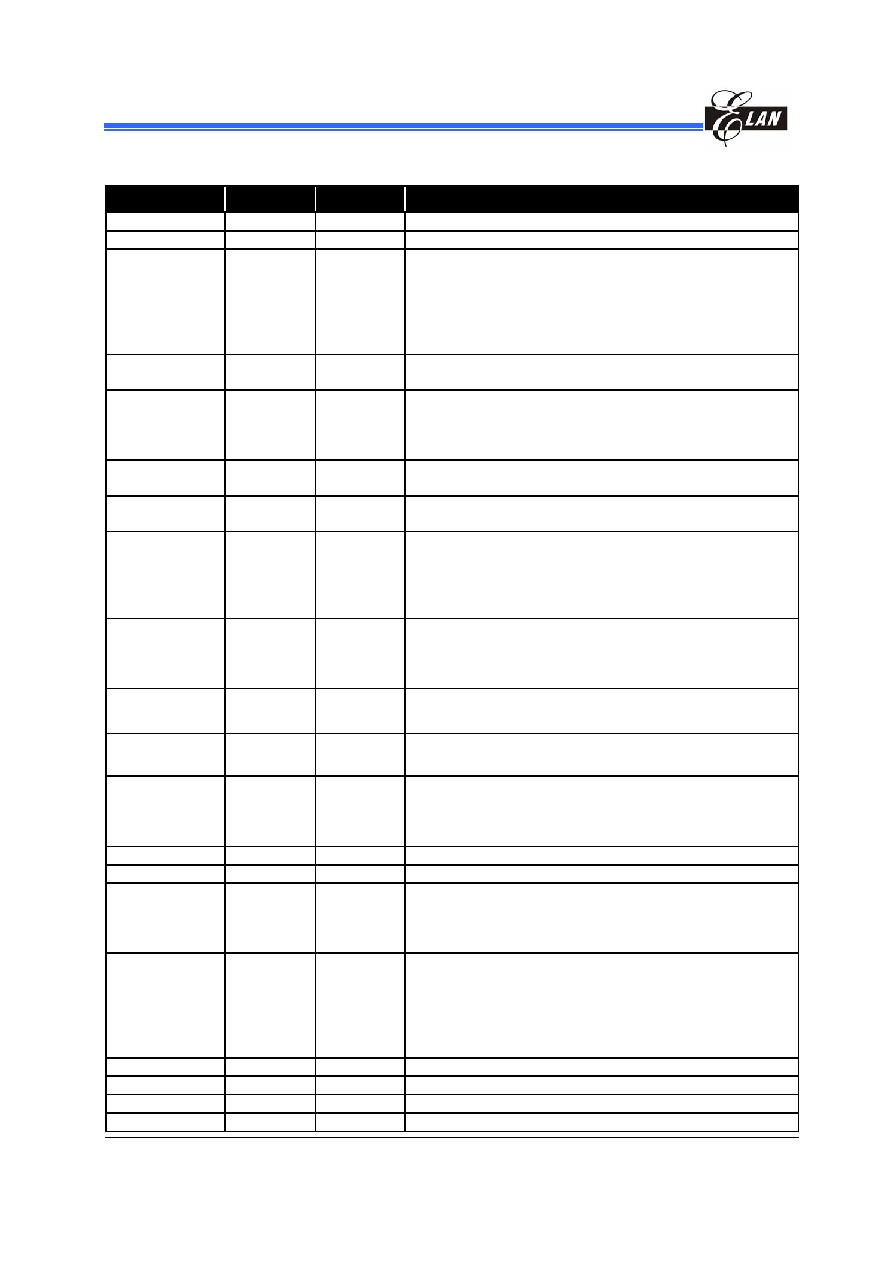
Table 1 (a) Pin Description for Package of QFP64 and LQFP64
PIN
PIN number
I/O type
Description
VDD
29
I
* Power supply pin
GND
26
I
* System ground pin
R-OSCI 27
I
* In crystal mode: crystal input
* In RC mode: resistor pull high.
* In PLL mode: connect 0.01
F capacitance to GND
* Connect 0.01
F capacitor to GND and code option select
PLL mode when high oscillator is not use.
OSCO 28 O
* In crystal mode: crystal output
* In RC mode: instruction clock output
Xin 30 I
* In crystal mode: Input pin for sub-oscillator. Connect to a
32.768KHz crystal
* RC mode: this pin is connected with a resistor to high
level.
Xout 31 O
* In crystal: Connect to a 32.768KHz crystal
* In RC mode: instruction clock output
/RESET 25
I
* Low active. If set as /RESET and remains at logic low, the
devices will be reset
P5.4/INT0 32
I/O
* General purpose I/O pin. /external interrupt.
* INT0 interruption source can be set to falling or rising
edge by IOC71 register bit 7 (INT_EDGE).
* Wake up from sleep mode and idle mode when the pin
status changes.
P5.5/INT1 33
I/O
* General purpose I/O pin. /external interrupt.
* Interruption source is a falling edge signal.
* Wake up from sleep mode and idle mode when the pin
status changes.
P5.6/TCC 34
I/O
* General purpose I/O/ external counter input
* This pin works in normal/green/idle mode.
P5.7/IROUT 37
I/O
* General purpose I/O pin or IR/PWM mode output pin,
* Capable of sinking 20mA/5V.
P6.0
~
P6.7
38~45
I/O
* General purpose I/O pin.
* Pull-high, pull-low and open drain function support.
* All pins can wake up from sleep and idle modes when the
pin status changes.
COM3~0
17~20
O
* LCD common output pin.
SEG0~SEG15
16~1
O
* LCD segment output pin.
SEG16/P7.0
~
SEG23/P7.7
64
~
57
O/(I/O)
* LCD segment output pin. Can be shared with general
purposes I/O pin
SEG24/P8.0
~
SEG30/P8.6
SEG31/P8.7
56
~
50
46
O/(I/O)
* LCD segment output pin. Can be shared with general I/O
pin
* For general purpose I/O use, can wake up from sleep
mode and idle mode when the pin status changes.
* For general purposes I/O use, supports pull-high
function.
VB
21
O
* Connect capacitors for LCD bias voltage
VA
22
O
* Connect capacitors for LCD bias voltage
VLCD2
23
O
* One of LCD bias voltage
VLCD3
24
O
* One of LCD bias voltage
NC
35~36
47~49
EM78P468N
8-BIT Microcontroller
8
�
Product Specification (V1.2) 03.15.2005
(This specification is subject to change without further notice)
Table 1 (b) Pin Description for Package of QFP44 and LQFP44
PIN
PIN number
I/O type
Description
VDD
18
I
* Power supply pin
GND
15
I
* System ground pin
R-OSCI 16 I
* In crystal mode: crystal input
* In RC mode: resistor pull high.
* In PLL mode: connect 0.01
F capacitance to GND
* Connect 0.01
F capacitor to GND and code option
select PLL mode when high oscillator is not use.
OSCO 17 O
* In crystal mode: crystal output
* In RC mode: instruction clock output
Xin 19 I
* In crystal mode: Input pin for sub-oscillator. Connect to a
32.768KHz crystal
* RC mode: this pin is connected with a resistor to high
level.
Xout 20 O
* In crystal: Connect to a 32.768KHz crystal
* In RC mode: instruction clock output
/RESET 14 I
* Low active. If set as /RESET and remains at logic low
* the devices will be reset
P5.4/INT0 21 I/O
* General purpose I/O pin. /external interrupt.
* INT0 interruption source can be set to falling or rising
edge by IOC71 register bit 7 (INT_EDGE).
* Wake up from sleep mode and idle mode when the pin
status changes.
P5.5/INT1 22 I/O
* General purpose I/O pin. /external interrupt.
* Interruption source is a falling edge signal.
* Wake up from sleep mode and idle mode when the pin
status changes.
P5.6/TCC 23 I/O
* General purpose I/O/ external counter input
* This pin works in normal/green/idle mode.
P5.7/IROUT 24
I/O
* General purpose I/O pin or IR/PWM mode output pin,
* Capable of sinking 20mA/5V.
P6.0
~
P6.7
25~32 I/O
* General purpose I/O pin.
* Pull-high, pull-low and open drain function support.
* All pins can wake up from sleep and idle modes when
the pin status changes.
COM3~0
6~9
O
* LCD common output pin.
SEG11~SEG14
5~2
O
* LCD segment output pin.
SEG16/P7.0
SEG17/P7.1
~
SEG23/P7.7
1
44
~
38
O/(I/O)
* LCD segment output pin. Can be shared with general
purposes I/O pin
SEG24/P8.0
~
SEG31/P8.4
37
~
33
O/(I/O)
* LCD segment output pin. Can be shared with general
I/O pin
* For general purpose I/O use, can wake up from sleep
mode and idle mode when the pin status changes.
* For general purposes I/O use, supports pull-high
function.
VB
10
O
* Connect capacitors for LCD bias voltage
VA
11
O
* Connect capacitors for LCD bias voltage
VLCD2
12
O
* One of LCD bias voltage
VLCD3
13
O
* One of LCD bias voltage

EM78P468N
8-BIT Microcontroller
4
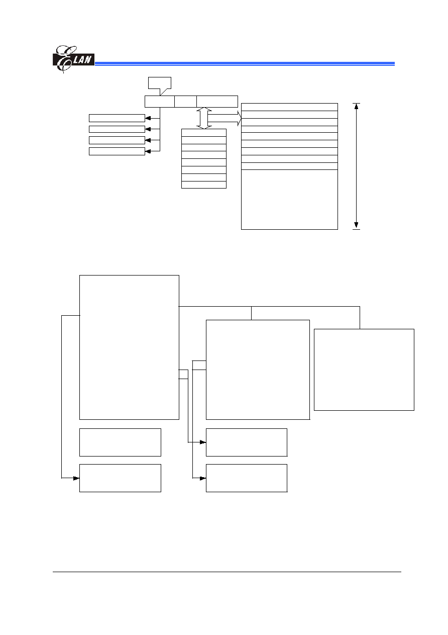
FUNCTION DESCRIPTION
Data RAM
LCD driver
IO PORT
IR/PWM
CPU
Timing Control
Timer/
Counter
ROM
I/O
LCD
Oscillator
PLL/Crystal/RC
Oscillator Timing
Product Specification
(V1.2) 03.15.2005
�
9
(This specification is subject to change without further notice)
Control
Data & Control BUS
PORT5
PORT6
PORT7
PORT8
128
Data RA
byte
M
General RAM
R 4
Instruction
decoder
WDT timer
ALU
ACC
R3
ROM
R2
STACK
Interruption
register
R1 (TCC)
Control w ake-up on I/
O port
Interruption
control
LCD RAM
IOC9
R
8
IOC9
R
7
IOC6
R
6
IOC5
R
5
Common
driver
R-
O
S
CI
OS
C
O
Xi
n
Xou
t
Segment
driver
Fig. 2 System Block Diagram

EM78P468N
8-BIT Microcontroller
10
�
Product Specification (V1.2) 03.15.2005
(This specification is subject to change without further notice)
4.1 Op
4.1
ess: 00h)
he data pointed by the RAM Select
4.1
Increases by an external signal edge applied to TCC, or by the instruction cycle clock.
Written and read by the program as any other register.
4.1.3
R2/PC (Program Counter)
(Address: 02h)
* The structure is depicted in Fig. 3
* Generates 4K
� 13 on-chip ROM addresses to the relative programming instruction
codes.
* "JMP" instruction allows direct loading of the low 10 program counter bits.
* "CALL" instruction loads the low 10 bits of the PC and PC+1, then push it into the stack.
* "RET'' ("RETL k", "RETI") instruction loads the program counter with the contents at the
top of stack.
* "MOV R2, A"
the A register to the PC. The
contents of the ninth and tenth bits do not change.
* "ADD R2, A" allows a relative address be added to the current PC.
* The most significa
t of bits PS0~PS1 in
the Status register (R3) upon execution of a "JMP'' or "CALL'' instruction.
erational Registers
.1 R0/IAR
(Indirect Addressing Register)
(Addr
R0 is not a physically implemented register. It is used as indirect addressing pointer. Any
instruction using R0 as register actually accesses t
Register (R4).
.2
R1/TCC (Time Clock Counter)
(Address: 01h)
allows the loading of an address from
nt bit (A10~A11) will be loaded with the conten
EM78P468N
8-BIT Microcontroller
A1
Product Specification
(V1.2) 03.15.2005
�
11
(This specification is subject to change without further notice)
1 A10 A9 A8 A7
~
A0
R3
PC
CAL
RET
L
RETL
RETI
00 PAGE0 0
03FF
000~
01 PAGE1 0400~07FF
10 PAGE2 0800~0BFF
11 PAGE3 0C00~0FFF
STACK LEVEL 1
STACK LEVEL 2
STACK LEVEL 3
STACK LEVEL 4
STACK LEVEL 5
STACK LEVEL 6
STACK LEVEL 7
STACK LEVEL 8
Reset v ector
000H
TCC ov erf l
errupt v ector
ow int
003H
Exteral INT
nterrupt v ecto
0 pin i
r
006H
Exteral INT1 pin interrupt v ector
Counter 1 underf low interrupt v ector
Counter 2 underf low interrupt v ector
high pulse width timer underf low interrupt v ector
low pulse width timer underf low interrupt v ector
Port 6,Port8 pin change wake-up interrupt v ector
009H
00CH
00FH
012H
015H
018H
On-Chip Program memory
FFFH
U
s
er
Me
m
o
r
y
S
p
ac
e
Fig. 3 Program Counter Organization
ADDRESS
0 1
0 0
0 3
0 2
0 5
0 4
0 7
0 6
0 9
0 8
0 B
0 A
0 D
0 C
0 F
0 E
IAR (Indirect Addressing Register)
lock Counter)
Counter)
TCC (Time C
PC (Program
SR (Status R
RSR (RAM s
PORT5 (Port
PORT6 (Port6 I/O data register)
PORT7 (Port7
PORT8 (Por
LCDCR (LC
LCD_ADDR
LCD_DB (L
CNTER (Cou
)
SBPCR (Sy
IRCR (IR, Pin of IR;INT0/1;TCC control)
ISR (interrup
R5 bit 0 -> 0
control register page 0
R5 bit 0 -> 1
control register page 1
egister)
elect register)
5 & IOCPAGE Control)
I/O data register)
t8 I/O data register)
D control register)
(LCD address)
CD data buffer)
nter enable register
stem, Booster , PLL control)
t status register)
16 byte
1 0
1 F
common register
ban
32 byte common register
|
2 0
3 F
|
ort5 I/O & LCD segment control)
P6CR (Port6 I/O c
l register)
R (Port7 I/O c
ol register)
(Port8 I/O c
l register)
_ADDR (128
RAM address)
RAM_DB (128 by
M data buffer)
CNT1PR (Counter
eset register)
CNT2PR (Counter
eset register)
HPWTPR (High-p
width timer preset)
LPWTPR (Low-pulse width timer preset)
P5CR (P
ontro
P7C
P8CR
ontr
ontro
RAM
byte
te RA
1 pr
2 pr
ulse
IMR (interrupt mask register)
k 0 ~ bank 3
128 byte data RAM
LCD RAM 4*32 bits
CNT12CR (Counter 1,2 control register)
6PH (Port 6 pull-high control register)
6OD (Port 6 open drain control register)
control register)
P6PL (Port 6 pull-low control register)
WUCR
nk current)
TCCCR
rol register)
DTCR (WDT control register)
LPWTCR (high/low pulse width timer control)
Mem
iguration
P
H
P
P8PH (Port 8 pull-high
(Wake up & P5.7 si
(TCC & INT0 cont
W
Fig. 4 Data
ory Conf

EM78P468N
8-BIT Microcontroller
12
�
Product Specification (V1.2) 03.15.2005
(This specification is subject to change without further notice)
4.1.4
R3/SR (Status Register)
(Address: 03h)
Bit 7
Bit 6
Bit 5
Bit 4
Bit 3
Bit 2
Bit 1
Bit 0
--
PS1
PS0
T P Z DC C
Bit 7 :
Bit 6 ~ 5 (PS
Pa
ct bits
Not used
1 ~ 0) :
ge sele
PS1
PS0
ROM page (Address)
0
0
Page 0 (000H ~ 3FFH)
0
1
Page 1 (400H ~ 7FFH)
1
0
Page 2 (800H ~ BFFH)
1
1
Page 3 (C00H ~ FFFH)
PS0~PS1 are used to select a ROM page. User can use PAGE instruction (e.g. PAGE 1)
or se
, "CALL", or other
instru
.g. MOV R2, A),
PS0~PS1 are loaded into the 11th and 12th bits of the program counter where it selects
RET (RETL, RETI) instruction
does
That is, the return will always be to the page from
wh
su
e w
d, r
rre
ing o
~PS
Bit
:
Tim
bit. S
1 by
LEP
"WD
mm
r duri
wer
t PS1~PS0 bits to change ROM page. When executing a "JMP"
ctions which causes the program counter to be changed (e
one of the available program memory pages. Note that
not change the PS0~PS1 bits.
ere the
broutin
as calle
egardless of the cu
nt sett
f PS0
1 bits.
4 (T)
e-out
et to
the "S
" and
TC" co
ands o
ng po
up and reset to 0 by WDT timeout.
EVENT
T
P
REMARK
WDT wake up from sleep mode
0
0
WD time out (not sleep mode)
0
1
T
/RESE
p
1
0
T wake up from slee
Po
1
1
wer up
Low pulse on /RESET
1
1
X: don't care
Bit 3 (P) :
Power down bit. Set to 1 during power on or by a "WDTC" command and reset
Bit 1 (
flag.
Bi
:
Ca
4.1.5
R4/RSR (RAM Select Register)
to 0 by a "SLEP" command.
Bit 2 (Z) :
Zero flag
DC) :
Auxiliary carry
t 0 (C)
rry flag
(Address: 04h)
Bit 7
Bit 6
Bit 5
Bit 4
Bit 3
Bit 2
Bit 1
Bit 0
RBS1 RBS0 RSR5 RSR4 RSR3 RSR2 RSR1 RSR0
Bits 7 ~ 6 (RBS1 ~ RBS0) :
determine which bank is activated among the 4 banks. See
the configuration of the data memory in Fig.4. Use BANK instruction (e.g. BABK 1) to
change bank.

EM78P468N
8-BIT Microcontroller
Product Specification
(V1.2) 03.15.2005
�
13
(This specification is subject to change without further notice)
Bits 5 ~ 0 (RSR5 ~ RSR0) :
are used to select up to 6
ct addressing mode.
4 registers (address: 00~3F) in the
indire
If no indirect addressing is used, the RSR can be used as an
8-
eral
ses
rite
er.
4.1.6
5/PO
(P
5
an Pa
l
bit gen
purpo
read/w
r regist
R
RT5
ORT I/O Data
d
ge of Register Se ect)
(Address: 05h)
Bit 7
Bit 6
Bit 5
Bit 4
Bit 3
Bit 2
Bit 1
Bit 0
R57 R56 R55 R54 --
--
-- IOCPAGE
Bit 7~4 :
4-bits I/O registers of PORT5
User can use IOC50 register to def
output each bit.
Bit 3~
Not used
Bit 0 (
PAGE) :
change IOC5 ~ I
other page
IOCPAGE = "0" :
Page 0 (select register of IOC 50 to IOC F0)
ect register of IOC 61 to IOC E1)
4.1.7
(PORT 6 I/O Data Register)
(Address: 06h)
ine input or
1 :
IOC
OCF to an
IOCPAGE = "1" :
Page 1 (sel
R6/PORT6
Bit 7
Bit 6
Bit 5
Bit 4
Bit 3
Bit 2
Bit 1
Bit 0
R67 R66 R65 R64 R63 R62 R61 R60
Bit 7~0 :
8-bit I/O registers of PORT 6
User
t or output each bit.
4.1.8
Register)
can use IOC60 register to define inpu
R7/PORT7 (PORT 7 I/O Data
(Address: 07h)
Bit 7
Bit 6
Bit 5
Bit 4
Bit 3
Bit 2
Bit 1
Bit 0
R77 R76 R75 R74 R73 R72 R71 R70
Bit 7
8-bit I/O registers
User can use IO 70 regi
or
4.1.9
8/POR
(PO
eg
~0 :
of PORT 7
C
ster to define input
output each bit.
R
T8
RT 8 I/O Data R
ister)
(Address: 08h)
Bit 7
Bit 6
Bit 5
Bit 4
Bit 3
Bit 2
Bit 1
Bit 0
R87 R86 R85 R84 R83 R82 R81 R80
Bi
8-bit
gist
OR
User can use IO 80 regis
to d
t
t 7~0 :
I/O re
ers of P
T 8
C
ter
efine inpu or output each bit.

EM78P468N
8-BIT Microcontroller
14
�
Product Specification (V1.2) 03.15.2005
(This specification is subject to change without further notice)
4.1
r)
.10 R9/LCDCR (LCD Control Registe
(Address: 09h)
Bit 7
Bit 6
Bit 5
Bit 4
Bit 3
Bit 2
Bit 1
Bit 0
BS DS1 S
LCDF0
D 0
LCDEN --
LCDTYPE LCDF1
Bit 7 (
LCD bias
ct bit,
1/2 bias
B
"1":
1/3 bias
Bit 6 ~ 5 (DS1 ~ DS
LCD dut select
BS):
sele
BS = "0":
S =
0):
y
DS1
DS0
LCD d y
ut
0 0 1/2
duty
0 1 1/3
duty
1 X 1/4
duty
Bit
it
DEN =
" :
LCD
cuit disa
. all
/s
nd
(GND) level
LCD circuit enable.
TY
0" :
DTYP
"1" :
B type waveform
me frequency control bits
4 (LCDEN) :
LCD enable b
LC
"0
cir
ble
common egment outputs are set to grou
LCDEN = "1" :
Bit 3:
Not used
Bit 2 (LCDTYPE) :
LCD drive waveform type select bit
LCD
PE = "
A type waveform
LC
E =
Bit 1 ~ 0(LCDF1 ~ LCDF0):
LCD fra
LCD frame frequency (e.g. Fs=32.768KHz)
LCDF1
LCDF0
1/2 duty
1/3 duty
1/4 duty
0 0 Fs/(256*2)=64.0
Fs/(172*3)=63.5
Fs/(128*4)
=64.0
0
.0
Fs/(140*4)
=58.5
1 Fs/(280*2)=58.5
Fs/(188*3)=58
1
.5
Fs/(152*4)
=53.9
0 Fs/(304*2)=53.9
Fs/(204*3)=53
1 1 Fs/(232*2)=70.6
Fs/(156*3)=70.0
Fs/(116*4)
=70.6
Fs: su
4.1.11
b-oscillator frequency
RA/LCD_ADDR (LCD Address)
(Address: 0Ah)
Bit 7
Bit 6
Bit 5
Bit 4
Bit 3
Bit 2
Bit 1
Bit 0
0
LCD_A1
LCD_A0
0 0
LCD_A4 LCD_A3 LCD_A2
Bit 7
~ 5:
Not used, fixed to "0"

EM78P468N
8-BIT Microcontroller
Product Specification
(V1.2) 03.15.2005
�
15
(This specification is subject to change without further notice)
Bit 4~0 (LCDA4 ~ LCDA0):
LCD RAM address
RB (LCD data buffer)
RA
(LCD address) Bit 7 ~4
Bit 3
(LCD_D3)
Bit 2
(LCD_D2)
Bit 1
(LCD_D1)
Bit 0
(LCD_D0)
Segmen
t
00H
--
SEG0
01H
--
SEG1
02H
--
SEG2
|
| |
1DH
--
SEG29
1EH
--
G30
SE
1FH
--
G31
SE
Common
X COM3 C
COM1 CO
OM2
M0
4.1.12 RB/LC _DB (L
Data Bu
Addre : 0Bh)
D
CD
ffer)
(
ss
Bit 7
Bit 6
Bit 5
Bit 4
Bit 3
Bit 2
Bit 1
Bit 0
-- -- -- --
LCD_D3 LCD_D2
LCD_D1
LCD_D0
Bit 7 ~ 4 :
Not used
Bit 3~0 (LCD_D3 ~ LCD_D0) :
LCD RAM data transfer register
4.1.13 RC/CNTER (Counter Enable Register)
(Address: 0Ch)
Bit 7
Bit 6
Bit 5
Bit 4
Bit 3
Bit 2
Bit 1
Bit 0
-- -- -- --
LPWTEN HPWTEN
CNT2EN
CNT1EN
Bit 7,
t used, must fixed to "0"
Bit 6,4
ot used
Bit 3(LPWTEN):
low pulse width timer enable b
LPWTEN = "0" :
Disa
PWT. Count operation stop.
LPWTEN = "1" :
Enable LPWT. Count operation start.
it
Count operation stop.
ount operation start.
Bit 1(CNT2EN) :
counter 2 enable bit
CNT2EN = "0" :
Disable Counter 2. Count operation stop.
CNT2EN = "1" :
Enable Counter 2. Count operation start.
Bit 0(CNT1EN) :
counter 1 enable bit
CNT1EN = "0" :
Disable Counter 1. Count operation stop.
5 :
No
:
N
it,
ble L
Bit 2(HPWTEN) :
high pulse width timer enable b
HPWTEN = "0" :
Disable HPWT.
HPWTEN = "1" :
Enable HPWT. C

EM78P468N
8-BIT Microcontroller
16
�
Product Specification (V1.2) 03.15.2005
(This specification is subject to change without further notice)
CNT1EN = "1" :
Enable Counter 1. Count operation start.
4.1.14 RD/SBPCR (System, Booster and PLL Control Register)
(Address: 0Dh)
Bit 7
Bit 6
Bit 5
Bit 4
Bit 3
Bit 2
Bit 1
Bit 0
-- CLK2
CLK1
CLK0
IDLE BF1 BF0
CPUS
Bit 7:
Not used
Bit 6 ~ 4 (CLK2 ~ CLK0):
main clock selection bits for PLL mode (code option select)
CLK2
CLK1
CLK0
Main clock
Example Fs=32.768K
0 0 0
Fs*130
4.26
MHz
0 0 1
Fs*65
2.13
MHz
0 1 0
Fs*65/2
1.065
MHz
0 1 1
Fs*65/4
532
KHz
1 X X
Fs*244
8
MHz
Bit 3 (IDLE) :
idle mode enable bit. This bit will decide the intended mode of the SLEP
instruction.
IDLE="0"+SLEP instr
* NOP
e added after SLEP instruction.
Ex
: IDL
ode
bit =
+SLEP instruc
ct
" +SLEP instruction + NOP instruction
Bit 2,1 (BF1,
uction => sleep mode
IDLE="1"+SLEP instruction => idle mode
instruction must b
ample
E m
: IDLE
"1"
tion + NOP instru ion
SLEEP mode : IDLE bit = "0
0):
LCD booster frequency select bit to adjust VLCD 2,3 driving.
BF1
BF0
Booster frequency
0 0 Fs
0 1 Fs/4
1 0 Fs/8
1 1 Fs/16
Bit 0
sub-o
CPUS = "0":
sub-oscillator (Fs)
(CPUS):
CPU oscillator source select, When CPUS=0, the CPU oscillator select
scillator and the main oscillator is stopped.
CPUS = "1":
main oscillator (Fm)

EM78P468N
8-BIT Microcontroller
Product Specification
(V1.2) 03.15.2005
�
17
(This specification is subject to change without further notice)
CPU Operation Mode
RESET
Code option
HLFS=1
Green Mode
fm:stop
fs: oscillation
CPU: using fs
Normal Mode
fs: oscillation
fm:oscillation
CPU: using fosc
IDLE Mode
fm:stop
CPU: stop
fs: oscillation
SLEEP M
Fm:stop
Fs: stop
CPU: stop
ode
IDLE
IDLE="0"
="1"
P
w ake up
SLE
SLEP
Wake up
CPUS="1"
CPUS="0"
Code option
HLFS=0
The w ake up time from idle to green
s 16*1/fs
mode i
The w ake up tim
approximately su
e from sleep to green mode is
b-oscillator setup time +18ms+16*1/fs
it must delay
oscillation stable w hile your system timing
control is conscienti
4.1.15 RE/IRCR (IR and PORT 5 Setting Control Register)
a little times for the main
ous
Fig. 5 CPU Operation Mode
(Address: 0Eh)
Bit 7
Bit 6
Bit 5
Bit 4
Bit 3
Bit 2
Bit 1
Bit 0
IRE HF LGP --
IR
E
OUTE
TCCE
INT1
EINT0
Bit 7 (IRE):
Infrared Remote Enable bit
pin is determined
r PWM function.
n. IROUT
e time as determined by
ly. The counter 2 is an
independent auto reload timer.
HF = "1" :
For IR application mode, enable H/W modulator function, the low time
lated with the frequency Fcarrier. The
d.
LGP = "1" :
The high-pulse width timer register is ignored. So the IROUT
waveform is dependent on low-pulse width timer register only.
IRE = "0" :
Disable IR/PWM function. The state of P5.7/IROUT
by bit 7 of IOC 50 if it's for IROUT.
IRE = "1" :
Enable IR o
Bit 6 (HF) :
High carry frequency.
HF = "0" :
For PWM application, disable H/W modulator functio
waveform is created according to high-pulse and low-puls
the high pulse and low pulse width timers respective
sections of the generated pulse is modu
frequency of Fcarrier provide by counter 2.
Bit 5 (LGP) :
IROUT for long time of low pulse.
LGP = "0" :
The high-pulse width timer register and low-pulse width timer is vali

EM78P468N
8-BIT Microcontroller
18
�
Product Specification (V1.2) 03.15.2005
(This specification is subject to change without further notice)
Bit 4 :
Not used
Bit 3 (IROUTE) :
Define the function of P5.7/IROUT pin.
l bit of P5.7 (bit 7 of IOC50)
T
l input pin of TCC, the control bit of P5.6 (bit 6 of IOC50)
m
Bit 1 (EINT1)
e th
ion of P5.5/INT1 pin.
1
n
ral
control bit of P5.5 (bit 5 of
IOC50) must be set to "1"
Bit 0
f
et to "1"
4.1.16
IROUTE = "0" :
for bi-directional general I/O pin.
IROUTE = "1" :
for IR or PWM output pin, the contro
must be set to "0"
Bit 2 (TCCE) :
Define the function of P5.6/TCC pin.
TCCE = "0" :
for bi-directional general I/O pin.
CCE = "1" :
for externa
ust be set to "1"
:
Defin
e funct
EINT = "0" :
for bi-directio al gene
I/O pin.
EINT1 = "1" :
for external interrupt pin of INT1, the
(EINT0) :
Define the function of P5.4/INT0 pin.
EINT0 = "0" :
for bi-directional general I/O pin.
EINT0 = "1" :
for external interrupt pin of INT0, the control bit of P5.4 (bit 4 o
IOC50) must be s
RF/ISR (Interrupt Status Register)
(Address: 0Fh)
Bit 7
Bit 6
Bit 5
Bit 4
Bit 3
Bit 2
Bit 1
Bit 0
ICIF LPWTF
HPWTF
CNT2F
CNT1F INT1F INT0F TCIF
Thes
Bit 7
ORT6,
pt flag of internal low-pulse width timer underflow.
Bit 5
w.
Bit 4
ernal INT1 pin interrupt flag.
Bit 1
Bit 0
.
se Register)
R1
F an
~R3
ks 0
e ge
urp
gist
e bits are set to "1" when interrupt occurs respectively.
(ICIF) :
PORT 6, PORT 8, input status changed interrupt flag. Set when P
PORT8 input changes.
Bit 6 (LPWTF) :
interru
(HPWTF) :
interrupt flag of internal high-pulse width timer underflo
(CNT2F) :
interrupt flag of internal counter 2 under-flow.
Bit 3 (CNT1F) :
interrupt flag of internal counter 1 underflow.
Bit 2 (INT1F ):
ext
(INT0F) :
external INT0 pin interrupt flag.
(TCIF) :
TCC timer overflow interrupt flag. Set when TCC timer overflows
4.1.17 Address: 10h~3Fh;R10~R3F (General Purpo
0~R31
d R20
F (Ban
~3) ar
neral p
oses re
er.

EM78P468N
8-BIT Microcontroller
Product Specification
(V1.2) 03.15.2005
�
19
(This specification is subject to change without further notice)
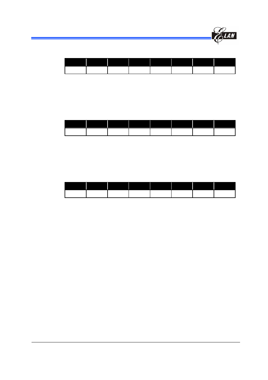
4.2 Sp
4.2.1
Regis
of I
age
C5
CF
0 o
= "
4.2.2
5
5
d
7,
C
e
ecial Purpose Registers
A
(Accumulator)
Internal data transfer, or instruction operand holding
This is not an addressable register.
ters
OC P
0 (IO
0 ~ IO
0, Bit
f R5
0")
IOC 0/P5CR (PORT I/O an PORT 8 for L D Segm nt
Control Register)
(Address: 05h, Bit 0 of R5 = "0")
Bit 7
Bit 6
Bit 5
Bit 4
Bit 3
Bit 2
Bit 1
Bit 0
IOC57 IOC56 IOC55 IOC54 P8HS P8LS P7HS P7LS
Bit
4(IOC57~54):
PORT 5 I/O direction control register
OC5x = "0":
set the relative P5.x I/O pins a
7~
x
et
ive
p
igh
nc
pi
t output as share
t output as share pins
SEGx
= "0
ct low nibble of PORT 8 as normal
P8LS = "1":
select LCD SEGMENT output as SEG 24~SEG 27 output
7HS):
Switch to high
f PORT 7 or to LCD segment output as share
.7
SEG
tput
B
e
L
ns
SEGxx/P7.x pins
rmal P7.0~P7.3
G 19 output
4.2.3
C60
R (
6
ntr
gis
ddr
06h
0 of
"0
I
s output
IOC5 = "1":
s the relat
P5.x I/O in into h
impeda e (input n)
Bit 3(P8HS):
Switch to high nibble I/O of PORT 8 or to LCD segmen
pins SEGxx/P8.x pins
P8HS = "0":
select high nibble of PORT 8 as normal P8.4~P8.7
P8HS = "1":
select LCD SEGMENT output as SEG 28~SEG 31 output
Bit 2(P8LS):
Switch to low nibble I/O of PORT 8 or to LCD segmen
x/P8.x pins
P8LS
":
sele
P8.0~P8.3
Bit 1(P
nibble I/O o
pins SEGxx/P7.x pins
P7HS = "0":
select high nibble of PORT 7 as normal P7.4~P7
P7HS = "1":
select LCD SEGMENT output as
20~SEG 23 ou
it 0(P7LS):
Switch to low nibbl I/O of PORT 7 or to CD segment output as share pi
P7LS = "0":
select low nibble of PORT 7 as no
P7LS = "1":
select LCD SEGMENT output as SEG 16~SE
IO
/P6C
PORT
I/O Co
ol Re
ter)
(A
ess:
, Bit
R5 =
")
Bit 7
Bit 6
Bit 5
Bit 4
Bit 3
Bit 2
Bit 1
Bit 0
IOC67 IOC66 IOC65 IOC64 IOC63 IOC62 IOC61 IOC60

EM78P468N
8-BIT Microcontroller
20
�
Product Specification (V1.2) 03.15.2005
(This specification is subject to change without further notice)
Bit 7 (IOC67)~Bit 0(IOC60):
PORT 6 I/O direction control register
IOC6x ="0":
set the relative PORT6.x I/O pins as output
edance (input pin)
4.2.4
C70
R (
7
ntr
gis
ddr
07h
0 of
"0
IOC6x ="1":
set the relative PORT6.x I/O pin into high imp
IO
/P7C
PORT
I/O Co
ol Re
ter)
(A
ess:
, Bit
R5 =
")
Bit 7
Bit 6
Bit 5
Bit 4
Bit 3
Bit 2
Bit 1
Bit 0
IOC77 IOC76 IOC75 IOC74 IOC73 IOC72 IOC71 IOC70
Bit 7 (IOC77)~Bit 0(IOC70):
PORT 7 I/O direction control register
IOC7x = "0":
set the relative PORT7.x I/O pins as output
4.2
)
(Address: 08h, Bit
IOC7x = "1":
set the relative PORT7.x I/O pin into high impedance (input pin)
.5
IOC80/P8CR (PORT 8 I/O Control Register
0 of R5 = "0")
Bit 7
Bit 6
Bit 5
Bit 4
Bit 3
Bit 2
Bit 1
Bit 0
IOC
3 IOC82 IOC81 IOC80
87 IOC86 IOC85 IOC84 IOC8
Bit 7 (IOC 87
(IOC 8
PORT 8 I/O dire
ster
IOC8x = "0":
set the relative PORT8.x I/O pins as output
4.2
)~Bit 0
0):
ction control regi
IOC8x = "1":
set the relative PORT8.x I/O pin into high impedance (input pin)
.6 IOC90/RAM_ADDR
(128
Bytes RAM Address)
(Address: 09h, Bit 0 of R5 = "0")
Bit 7
Bit 6
Bit 5
Bit 4
Bit 3
Bit 2
Bit 1
Bit 0
0
RAM_A6 RAM_A5 RAM_A4 RAM_A3 RAM_A2 RAM_A1 RAM_A0
Bit 7:
Not used,
Bit 6~0:
128 bytes RAM address
4.2.7
ata Buffer)
ddr
0Ah
0 o
"0
fixed at "0"
IOCA0/RAM_DB (128 Bytes RAM D
(A
ess:
, Bit
f R5 =
")
Bit 7
Bit 6
Bit 5
Bit 4
Bit 3
Bit 2
Bit 1
Bit 0
RAM_D7 RAM_D6 RAM_D5 RAM_D4 RAM_D3 RAM_D2 RAM_D1 RAM_D0
Bit 7~0:
128 bytes RAM data transfer register
.8
IOCB0/CNT1PR (Counter 1 Preset Register)
(Address: 0Bh, Bit 0 of R5 = "0")
4.2
Bit 7
Bit 6
Bit 5
Bit 4
Bit 3
Bit 2
Bit 1
Bit 0
Bit 7
Bit 6
Bit 5
Bit 4
Bit 3
Bit 2
Bit 1
Bit 0
Bit 7 ~ Bit 0:
All are Counter 1
read and write. The Counter 1 is an
8-bit down-count timer with 8-bit pre-scaler that is used as this register to preset the
buffer that user can

EM78P468N
8-BIT Microcontroller
counter and read preset value. The pre-scaler is s
ption, it will auto reload the preset value.
et by IOC91 register. After an
interru
4.2.9
nter 2 Preset Register)
dd
C
"
IOCC0/CNT2PR (Cou
(A
ress: 0 h, Bit 0 of R5 = 0")
Bit 7
Bit 6
Bit 5
Bit 4
Bit 3
Bit 2
Bit 1
Bit 0
B
Bit 4
Bit 3
Bit 2
Bit 1
Bit 0
it 7
Bit 6
Bit 5
Bit 7
nter 2 buffer that user can read and write. The Counter 2 is an
8-bit down-count timer with 8-bit pre-scaler that is used as this register to preset the
e-scaler is set by IOC91 register. After an
n
If the Counter 2 clock source is equal to F
T
�
~ Bit 0:
All are Cou
counter and read preset value. The pr
interruption, it will reload the preset value.
Whe IR output is enabled, this control register can obtain carrier frequency output.
Carrier frequency (Fcarrier) =
presc
*
aler
)
1
+
_
set
2
F
T
4.2.10 IOCD0/HPWTPR High-P se
i
s
value
pre
(
*
(
ul
Width T mer Preset Regi ter)
(Address: 0Dh, Bit 0 of R5 = "0")
Bit 7
Bit 6
Bit 5
Bit 4
Bit 3
Bit 2
Bit 1
Bit 0
Bit 7
Bit 5
Bit 3
Bi
t 1
Bit 0
Bit 6
Bit 4
t 2
Bi
Bit 7 ~ Bit
All are high-pulse
imer buffer that
an read and write.
High-pulse w th timer preset regis
eight-bit down-
ith 8-bit pre-scaler
0 to preset the counter and read preset value. The pre-scaler is set
interruption, it will reload the preset value.
0:
width t
user c
id
ter is an
counter w
that is used as IOCD
by IOCA1 register. After an
For PWM or IR application, this control register is set as high pulse width.
If the high-pulse width timer source clock is F �
T
Product Specification
(V1.2) 03.15.2005
�
21
(This specification is subject to change without further notice)
High pulse time =
T
F
)
1
+
value
_
preset
(
*
prescaler
4.2.11 IOCE0/LPWTPR (Low-Pulse Width Timer Preset Register)
(Address: 0Eh, Bit 0 of R5 = "0")
Bit 7
Bit 6
Bit 5
Bit 4
Bit 3
Bit 2
Bit 1
Bit 0
Bit 7
Bit 6
Bit 5
Bit 4
Bit 3
Bit 2
Bit 1
Bit 0
Bit
t 0:
All are low-p
idth
buff
use
ad
ite.
lse
eset is an eig
t down-counter
it
r
e
0
to preset the counter and read preset value. The pre-scaler is set by IOCA1 register.
it will reload the preset value.
For P
width.
If the
7 ~ Bi
ulse w
timer
er that
r can re
and wr
Low-pu
width timer pr
ht-bi
with 8-b pre-scale that is us d as IOCE
After an interruption,
WM or IR application, this control register is set as low pulse
low-pulse width timer source clock is F
T
�

EM78P468N
8-BIT Microcontroller
22
�
Product Specification (V1.2) 03.15.2005
(This specification is subject to change without further notice)
Low pulse time =
T
F
)
4.2
t Mask Register)
1
+
value
_
preset
(
*
prescaler
.12 IOCF0/IMR
(Interrup
(Address: 0Fh, Bit 0 of R5 = "0")
Bit 7
Bit 6
Bit 5
Bit 4
Bit 3
Bit 2
Bit 1
Bit 0
ICIE LPWTE
HPWTE
CNT2E
CNT1E INT1E INT0E TCIE
Bit 7~Bit 0:
interrupt enable bit. Enable interrupt source respectively.
Registers of IOC Page 1 (IOC61 ~ IOCE1, Bit 0 of 5 = "1")
4.2.13 IOC61/WUCR (Wake Up and sink current of P5.7/IROUT Control
Register)
(Address: 06h
it 0 of R5 =
")
0:
disable interrupt
1:
enable interrupt
IOCF0 register is readable and writable.
R
, B
"1
Bit 7
Bit 6
5
Bit 4
Bit 3
Bit 2
Bit 1
Bit
Bit 0
IROCS --
--
/WUE8L
/WUE6H E6L
--
/WUE8H
/WU
Bit 7:
IROCS: IROUT/PORT5.7 output sink current set
P5.7/IROUT Sink current
IROCS
VDD=5V
VDD=3V
0
10 mA
6 mA
1
20 mA
12 mA
Bit 6,5,4:
Not
Bit 3 (/WUE8H):
0/1=> enable/disable P8.4~P8.7 pin change wake up function
Bit 2 (/WUE8L):
0/1=> enable/disable P8.0~P8.3 pin change wake up function
UE6H):
0/1=> enable/disable P6.4~P6.7 pin change wake up function
Bit 0
~P6.3 pin change wake up function
* Por
ting when wakeup function is enabled.
The initial state of wakeup function is enabled.
4.2.14 IOC71/TCCCR (TCC Control Register)
(Address: 07h, Bit 0 of R5 = "1")
used
Bit 1 (/W
(/WUE6L):
0/1=> enable/disable P6.0
t 6 and Port 8 must avoid input floa
Bit 7
Bit 6
Bit 5
Bit 4
Bit 3
Bit 2
Bit 1
Bit 0
INT_EDGE INT
TS
TE
PSRE TCCP2 TCCP1 TCCP0
Bit 7 (INT_EDGE):
INT_EDGE = "0":
Interrupt on rising edge of P5.4/INT0 pin

EM78P468N
8-BIT Microcontroller
Product Specification
(V1.2) 03.15.2005
�
23
(This specification is subject to change without further notice)
I
= "1":
Inte
lling edge of P5.4/INT0 pin
Bit 6 (INT
NT enable flag, this bit is read only
INT
0":
interrupt mask
wa
nterrupt
INT
1":
interrupt enabl
ons
Bit 5 (TS)
CC signal source
TS = "0":
internal instruct
cycle clock
TS = "1":
transition on TCC pin, TCC period >
rnal instruction c
eriod
Bit 4 (TE):
TCC signal edge
me
CC
ing
B
S
0
e
ts
NT_EDGE
rrupt on fa
):
I
= "
ed by DISI or hard
re i
= "
ed by ENI/RETI instructi
:
T
ion
inte
lock p
TE = "0":
increment by TCC pin rising edge
TE = "1":
incre
nt by T
pin fall
edge
it 3~0 (P RE,TCCP2 ~ TCCP ):
TCC pr -scaler bi .
PSRE
TCCP2
TCCP1
TCCP0
TCC rate
0 X X X 1:1
1 0 0 0 1:2
1 0 0 1 1:4
1 0 1 0 1:8
1 0
1 1 1:16
1 1
0 0 1:32
1 1
0 1 1:64
1 1
1 0
1:128
1 1
1 1
1:256
4.2.15 IOC81/WDTCR (WDT Control R gister)
(Address: 08h, Bit 0 of R5 = "1")
e
Bit 7
Bit 6
Bit 5
Bit 4
Bit 3
Bit 2
Bit 1
Bit 0
-- -- -- --
WDTE
WDTP2
WDTP1
WDTP0
Bit
sed
7 ~ 4:
Not u
Bit 3 (W
E):
watchdog timer enable. This control bit is used
nable the Watchdog
timer,
W
E = "0":
Disable WDT function.
WD
":
enable WDT function.
DT
to e
DT
TE = "1

EM78P468N
8-BIT Microcontroller
24
�
Product Specification (V1.2) 03.15.2005
(This specification is subject to change without further notice)
Bit 2 ~ 0 (WDTP2 ~ WDTP0)
: watchdog timer pre-scaler bits. The WDT source
scillation frequ
clock is
sub-o
ency.
WDTP2
WDTP1
WDTP0
WDT rate
0 0 0 1:1
0 0 1 1:2
0 1 0 1:4
0 1 1 1:8
1 0 0
1:16
1 0 1
1:32
1 1 0
1:64
1 1 1
1:128
4.2.16 IOC91/CNT12CR unter
1,
ontrol Register
(Address: 09h, t 0 of R5 = "
(Co
2 C
)
Bi
1")
Bit 7
Bit 6
Bit 5
Bit 4
Bit 3
Bit 2
Bit 1
Bit 0
CNT2S CNT2P2 CN
P1 CNT2P0
NT1S CNT1P2 C
1 CNT1P0
T2
C
NT1P
Bit 7(CN
S):
Counter 2
source selec /1 => Fs/ Fm*
(*Fs: sub-oscillator clock, Fm: main-oscillator clock)
T2
clock
t 0
Bit 6~4(CNT2P2 ~ CNT2P 0):
Counter 2 pre-scaler select bits
CNT2P2
CNT2P1
CNT1P0
Counter 2 scale
0 0 0
1:2
0 0 1
1:4
0 1 0
1:8
0 1 1
1:16
1 0 0
1:32
1 0 1
1:64
1 1 0
1:128
1 1 1
1:256
Bit 3(CNT1S):
Counter 1 clock source select 0/1 => Fs/ Fm*
~
Bit 2 0 (CNT1P2 ~ CNT1P20):
Counter 1 pre-scaler select bits
CNT1P2
CNT1P1
CNT1P0
Counter 1 scale
0 0 0
1:2
0
:4
0 1
1
0 1 0
1:8
0 1 1
1:16
1 0 0
1:32
1 0 1
1:64
1 1 0
1:128
1 1 1
1:256

EM78P468N
8-BIT Microcontroller
Product Specification
(V1.2) 03.15.2005
�
25
(This specification is subject to change without further notice)
4.2.17 IOCA1/HLPWTCR
(High/Low
Pulse Width Timer Contr
Register)
ol
ddr
0Ah
0 o
"1
(A
ess:
, Bit
f R5 =
")
Bit 7
Bit 6
Bit 5
Bit 4
Bit 3
Bit 2
Bit 1
Bit 0
LPWTS LPWTP2 LPWTP1 LPWTP0 HPWTS HPWTP2 HPWTP1 HPWTP0
Bit 7
m*
(*Fs:
~
(LPWTS):
low-pulse width timer clock source select 0/1 -> Fs/ F
sub-oscillator clock, Fm: main-oscillator clock)
Bit 6 4 (LPWTP2~ LPWTP0):
low-pulse width timer pre-scaler select bits
LPWTP2
LPWTP1
LPWTP0
Low-pulse width timer scale
0 0 0
1:2
0
1
0
1:4
0
0
1
1:8
0 1 1
1:16
1 0 0
1:32
1 0 1
1:64
1 1 0
1:128
1 1 1
1:256
Bit 3(
e select 0/1 -> Fs/ Fm*
Bit 2
W
WT
high
dth timer pre
select bits
HPWTS):
high-pulse width timer clock sourc
~0(HP TP2~ HP
P0):
-pulse wi
-scaler
HPWTP2
HPWTP1
HPWTP0
High-p lse w
u
idth timer scale
0 0 0
1:2
0 0 1
1:4
0 1 0
1:8
0 1 1
1:16
1 0 0
1:32
1 0 1
1:64
1 1 0
1:128
1 1 1
1:256
4.2.18 IOCB1/P6PH (PORT 6 Pull High Control Register)
(Address: 0Bh, Bit 0 of R5 = "1")
Bit 7
Bit 6
Bit 5
Bit 4
Bit 3
Bit 2
Bit 1
Bit 0
PH67 PH66 PH65 PH64 PH63 PH62 PH61 PH60
Bit 7 ~ Bit 0 (PH67 ~ PH60):
The enable bits of PORT 6 pull high function.
PH6x = "0":
disable pin of P6.x internal pull-high resistor function
PH6x = "1":
enable pin of P6.x internal pull-high resistor function
EM78P468N
8-BIT Microcontroller
26
�
Product Specification (V1.2) 03.15.2005
(This specification is subject to change without further notice)
4.2.19 IOCC1/P6OD (PORT 6 Open Drain Control Register)
(Address: 0Ch, Bit 0 of R5 = "1")
Bit 7
Bit 6
Bit 5
Bit 4
Bit 3
Bit 2
Bit 1
Bit 0
OP67 OP66 OP65 OP64 OP63 OP62 OP61 OP60
Bit 7 ~ Bit 0:
The enable bits of PORT 6 open drain function.
OD6x = "0":
disable pin of P6.x open drain function
OD6x = "1":
enable pin of P6.x open drain function
4.2.20 IOCD1/P8PH (PORT 8 Pull High Control Register)
(Address: 0Dh, Bit 0 of R5 = "1")
Bit 7
Bit 6
Bit 5
Bit 4
Bit 3
Bit 2
Bit 1
Bit 0
PH87 PH86 PH85 PH84 PH83 PH82 PH81 PH80
Bit 7 ~ Bit 0:
The enable bits of PORT 8 pull-high function.
PH8x = "0":
disable pin of P8.x internal pull-high resistor function
PH8x = "1":
enable p
n
4.2.21 IOCE1/P6PL (PORT 6 Pull-Low Control Register)
(Address: 0Eh, Bit 0 of R5 = "1")
in of P8.x pull-high resistor functio
Bit 7
Bit 6
Bit 5
Bit 4
Bit 3
Bit 2
Bit 1
Bit 0
PL67 PL66 PL
PL61 PL60
65 PL64 PL63 PL62
Bit 7 ~ Bit 0:
The enable bits of PORT 6 pull low function.
PL6x = "0":
disable pin of P6.x internal pull-low resistor function
PL6x = "1":
enable pin of P6.x internal pull-low resistor function
4.3 TCC and WDT Pre-scaler
Two 8-bit counters are available as pre-scalers for the TCC (Time Clock Counter) and
WDT (Watch Dog Timer). The TCCP2~TCCP0 bits of the IOC71 register are used to
determine the ratio of the TCC pre-scaler. Likewise, the WDTP2~WDTP0 bits of the
IOC81 register are used to determine the WDT pre-scaler. The TCC pre-scaler
(TCCP2~TCCP0) is cleared by the instructions each time they are written into TCC,
while the WDT pre-scaler is cleared by the "WDTC" and "SLEP" instructions. Fig.7
depicts the circuit diagram of TCC and WDT.
R1 (TCC) is an 8-bit timer/counter. The clock source of TCC can be selected by internal
instruction clock or external signal input (edge selectable from the TCC control register).
If TCC signal source is from internal instruction clock, TCC will increase by 1 at every
instruction cycle (without pre-scaler). If TCC signal source is from external clock input,
TCC will increase by 1 at every falling edge or rising edge of the TCC pin.
The watchdog timer is a free running on sub-oscillator. The WDT will keep on running
even after the oscillator driver has been turned off. During Normal mode, Green mode, or

EM78P468N
8-BIT Microcontroller
Idle mode operation, a WDT time-out (if enabled) will cause the device to reset. The
WDT can be enabled or disabled at any time during the Normal mode and Green mode
by software programming. Refer to WDTE bit of IOC81 register. The WDT time-out
period is equal to (pre-scaler*256/ (Fs/2)).
TCC
Pin
MUX
Instruction Clock = Fosc /2
Fosc: CPU operate frequency
TCC (R1)
Prescaler
TCCP2~0
(IOC71)
8 to 1 MUX
TE (IOC71)
Data Bus
TCC overflow interrupt
PSRE
(IOC71)
TS (IOC71)
Fig. 7(a) Block Diagram of TCC
8 bit counter
WDT
Prescaler
WDTP2~0
(IOC81)
Fs/2
(Fs:Sub oscillator)
8 to 1 MUX
WDT Time out
WDTE (IOC81)
Fig. 7(b) Block Diagram of WDT
Product Specification
(V1.2) 03.15.2005
�
27
(This specification is subject to change without further notice)
EM78P468N
8-BIT Microcontroller
28
�
Product Specification (V1.2) 03.15.2005
(This specification is subject to change without further notice)
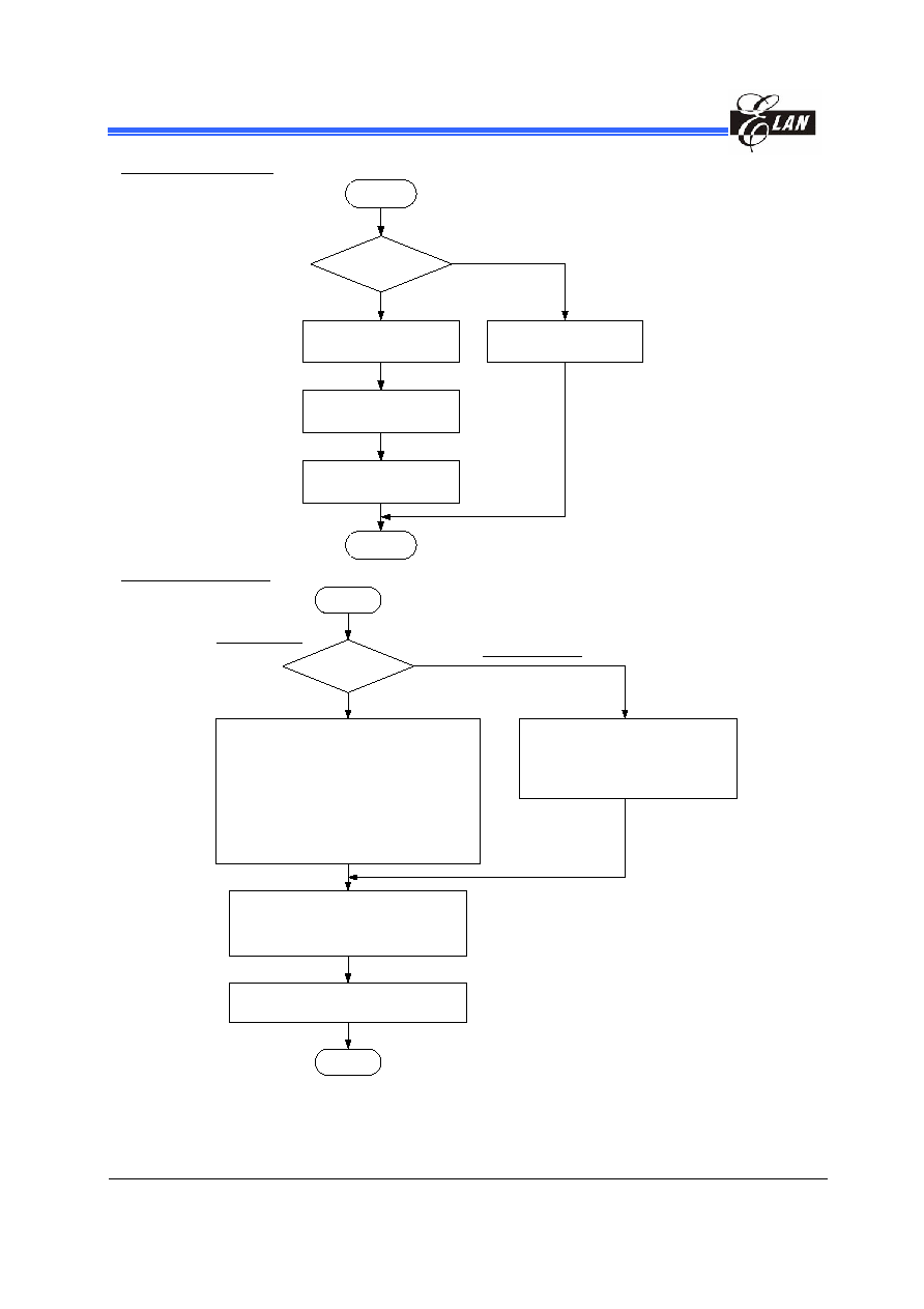
WDT setting flowchart
N
START
Use WDT function ?
Y
Setting WDT prescaler
(IOC81 register)
Enable WDT
(bit 3 of IOC81)
END
Enable WDT function : set bit 7 of
Code option Word 0 to "0"
Disable WDT function : set bit 7 of
Code option Word 0 to "1"
WDTtime= prescaler*256/Fs
Fs: sub-oscillator frequency
TCC setting flowchart
from External Input
START
TCC clock source?
External/ instruction cycle
*set clock source from external TCC pin
(set bit 4 of IOC71 to "1")
*set P5.6/TCC for TCC input Pin
( set bit 2 of RE to "1" and set bit 6 of IOC 50 to "1")
*choose TCC pin operation edge
(set by bit 4 of IOC71)
*choose TCC prescaler
(set by bit 0 to bit 3 of IOC71)
END
*choose TCC clock source from instruction cycle
(set bit 4 of IOC71 to "0")
*choose TCC prescaler
(set by bit 0 to bit 3 of IOC71)
from Instruction Cycle
Enable TCC to start count
(use ENI instruction)
* Enable TCC interrupt Mask
(set bit 0 of IOCF0 to "1")
*Clear TCC interrupt Flag
(set bit 0 of RF to "0")

EM78P468N
8-BIT Microcontroller
4.4 I/O Ports
The I/O registers, (PORT 5, PORT 6, PORT 7and PORT 8), are bi-directional tri-state I/O
are pulled-high internally by software; PORT 6 is also
pulled-low int
urthermore, PORT 6 has its open-drain output also
PORT 8 features an input status changed interrupt (or
ke
ed-high by software. Each I/O pin can be defined as "input"
O
n in
ports. PORT 6 and PORT 8
ernally by software. F
through software. PORT 6 and
wa -up) function and is pull
or "output" pin by the I/O control register (IOC50 ~ IOC80). The I/O registers and I/
control registers are both readable and writable. The I/O interface circuits are show
Fig. 8
NOTE: Open-drain, pull high, and pull down are not shown in the figure.
Fig. 8 The Circuit of I/O Port and I/O Control Register for PORT 5 ~ 8
Product Specification
(V1.2) 03.15.2005
�
29
(This specification is subject to change without further notice)

EM78P468N
8-BIT Microcontroller
30
�
Product Specification (V1.2) 03.15.2005
(This specification is subject to change without further notice)
4.5 RESET
A reset c
tivate
Re t)
WDT timeout. (if enabled)
/RESET pin go to low.
Note
ese ircuit is lways
abled. It will reset CP at ab
1.9V
Once re
, the
ing
o
p
e
run ng, or will be started.
The program cou
2/
s
l "
are
nfigured as in t mode (high-i
nce state
The TCC/Watchdog timer a
, th
it 5, 6 of R3 and the u
r 2 b of R4
e cleared.
1 re ster are set to
"1" e
pt for
t 6 (IN flag).
Fo
sters, see Table 2 belo
and Wake-up
an be ac
d by
POR (Power On
se
: The power on r
t c
a
en
U
out
.
set occurs
fo w
llo
fu cti
n
ns re
a
erf m
or
d
The oscillator is
ni
nter (R PC) is et to al 0".
All I/O port pins
co
pu
mpeda
).
nd pre-scaler are cleared.
When power on
e B
ppe
its
ar
Bits of the IOC7
gi
all
xce
Bi
T
r other regi
w.

EM78P468N
8-BIT Microcontroller
Product Specification
(V1.2) 03.15.2005
�
31
(This specification is subject to change without further notice)
T
mar
he
liz
lu
R
rs
able 2 Sum
y of t
Initia ed Va es for egiste
Address
Name
R
eset Type
Bit 7
Bit 6
Bit 5
Bit 4
Bit 3
Bit 2
Bit 1
Bit 0
Bit Name
IOC57
IOC56
IOC55
IOC54
P8HS
P8LS
P7HS
P7LS
Power-On 1 1 1 1 0 0 0 0
/RESET
and
WDT
1 1 1 1 0 0 0 0
0x05
(P5CR)
Wake-Up from Pin
IOC50
Change
P P P P P P P P
Bit Name
IOC67
IOC66
IOC65
IOC64
IOC63
IOC62
IOC61
IOC60
Power-On
1
1
1
1 1 1 1 1
/RESET and WDT
1
1
1
1 1 1 1 1
0x06
(P6CR)
Wake-Up from Pin
IOC60
Change
P
P
P
P P P P P
Bit Name
IOC77
IOC76
IOC75
IOC74
IOC73
IOC72
IOC71
IOC70
Power-On 1 1 1 1 1 1 1 1
/RESET
and
WDT
1 1 1 1 1 1 1 1
0x07
(P7CR)
Wake-Up from Pin
IOC70
Change
P P P P P P P P
Bit Name
IOC87
IOC86
IOC85
IOC84
IOC83
IOC82
IOC81
IOC80
Power-On 1 1 1 1 1 1 1 1
/RESET
and
WDT
1 1 1 1 1 1 1 1
0x08
(P8CR)
Wake-Up from Pin
IOC80
Change
P P P P P P P P
Bit Name
X
RAM_A6 RAM_A5 RAM_A4 RAM_A3 RAM_A2 RAM_A1
RAM_A0
Power-On 0 0 0 0 0 0 0 0
/RESET
and
WDT
0 0 0 0 0 0 0 0
0x09
(RAM_ADD
R)
Wake-Up from Pin
IOC90
Change
P P P P P P P P
Bit Name
RAM_D7
RAM_D6 RAM_D5 RAM_D4 RAM_D3 RAM_D2 RAM_D1 RAM_D0
Power-On U U U U U U U U
/RESET
and
WDT
P P P P P P P P
0x0A
(RAM_DB)
Wake-Up from Pin
IOCA0
Change
P P P P P P P P
Bit Name
Bit 7
Bit 6
Bit 5
Bit 4
Bit 3
Bit 2
Bit 1
Bit 0
Power-On 0 0 0 0 0 0 0 0
/RESET
and
WDT
0 0 0 0 0 0 0 0
0x0B
(CNT1PR)
Wake-Up from Pin
IOCB0
Change
P P P P P P P P
Bit Name
Bit 7
Bit 6
Bit 5
Bit 4
Bit 3
Bit 2
Bit 1
Bit 0
Power-On 0 0 0 0 0 0 0 0
/RESET
and
WDT
0 0 0 0 0 0 0 0
0x0C
(CNT2PR)
Wake-Up from Pin
IOCC0
Change
P P P P P P P P
Bit Name
Bit 7
Bit 6
Bit 5
Bit 4
Bit 3
Bit 2
Bit 1
Bit 0
Power-On 0 0 0 0 0 0 0 0
/RESET
and
WDT
0 0 0 0 0 0 0 0
0x0D
(HPWTPR)
Wake-Up from Pin
IOCD0
Change
P P P P P P P P
Bit Name
Bit 7
Bit 6
Bit 5
Bit 4
Bit 3
Bit 2
Bit 1
Bit 0
Power-On 0 0 0 0 0 0 0 0
/RESET
and
WDT
0
0
0 0 0 0 0 0
0x0E
(LPWTPR)
Wake-Up from Pin
IOCE0
Change
P P P P P P P P
Bit Name
ICIE
LPWTE HPWTE CNT2E
CNT1E
INT1E
INT0E
TCIE
Power-On 0 0 0 0 0 0 0 0
/RESET
and
WDT
0 0 0 0 0 0 0 0
0x0F
(IMR)
Wake-Up from Pin
IOCF0
Change
P P P P P P P P
Bit Name
IROCS
X
X
X
/WUE8H /WUE8L /WUE6H /WUE6L
Power-On 0 U U U 0 0 0 0
/RESET and WDT
0
U
U
U
0
0
0
0
0x06
(WUCR)
Wake-Up from Pin
IOC61
Change
P U U U P P P P
Bit Name
INT_EDGE
INT
TS
TE
PSRE
TCCP2 TCCP1 TCCP0
Power-On 1 0 1 1 1 1 1 1
/RESET
and
WDT
1 0 1 1 1 1 1 1
0x07
(TCCCR)
Wake-Up from Pin
Change
IOC71
P P P P P P P P

EM78P468N
8-BIT Microcontroller
32
�
Product Specification (V1.2) 03.15.2005
(This specification is subject to change without further notice)
Address
Name
Reset Type
Bit 7
Bit 6
Bit 5
Bit 4
Bit 3
Bit 2
Bit 1
Bit 0
Bit Name
X
X
X
X
W
DTE
WDTP2 WDTP1 WDTP0
Power-On U U U U 0 1 1 1
/RESET and WDT
U
U
U
U
0
1
1
1
0x08
IOC81
(WDTCR)
Wake-Up from Pin
Change
U U U U P P P P
Bit Name
CNT2S
CNT2P2 CNT2P1 CNT2P0 CNT1S CNT1P2 CNT1P1 CNT1P0
Power-On 0 0 0 0 0 0 0 0
/RESET
and
WDT
0 0 0 0 0 0 0 0
0x09
IOC91
(CNT12CR)
W
ake-Up from Pin
Change
P P P P P P P P
Bit Name
LPWTS LPWTP2 LPWTP1 LPWTP0 HPWTS
H
PWTP2 H
1
PWTP
H
0
PWTP
Power-On 0 0 0 0 0 0 0 0
/RESET
and
WDT
0 0 0 0 0 0 0 0
0x0A
IOCA1
HLPWTCR)
(
Wake-Up from Pin
Change
P P P P P P P P
Bit Name
PH67
PH66
PH65
PH64
PH63
PH62
PH61
PH60
Power-On 0 0 0 0 0 0 0 0
/RESET
and
WDT
0 0 0 0 0 0 0 0
0x0B
IOCB1
(P6PH)
Wake-Up from Pin
Change
P P P P P P P P
Bit Name
OP67
OP66
OP65
OP64
OP63
OP62
OP61
OP60
Power-On 0 0 0 0 0 0 0 0
/RESET
and
WDT
0 0 0 0 0 0 0 0
0x0C
IOCC1
(P6OD)
Wake-Up from Pin
Change
P P P P P P P P
Bit Name
PH87
PH86
PH85
PH84
PH83
PH82
PH81
PH80
Power-On 0 0 0 0 0 0 0 0
/RESET
and
WDT
0 0 0 0 0 0 0 0
0x0D
IOCD1
(P8PH)
Wake-Up from Pin
Change
P P P P P P P P
Bit Name
PL67
PL66
PL65
PL64
PL63
PL62
PL61
PL60
Power-On 0 0 0 0 0 0 0 0
/RESET
and
WDT
0 0 0 0 0 0 0 0
0x0E
IOCE1
(P6PL)
Wake-Up from Pin
Change
P P P P P P P P
Bit Name
Bit 7
Bit 6
Bit 5
Bit 4
Bit 3
Bit 2
Bit 1
Bit 0
Power-On U U U U U U U U
/RESET
and
WDT
P P P P P P P P
0x00
R0
(IAR)
Wake-Up from Pin
Change
P P P P P P P P
Bit Name
Bit 7
Bit 6
Bit 5
Bit 4
Bit 3
Bit 2
Bit 1
Bit 0
Power-On 0 0 0 0 0 0 0 0
/RESET
and
WDT
0 0 0 0 0 0 0 0
0x01
R1
(TCC)
Wake-Up from Pin
Change
P P P P P P P P
Bit Name
Bit 7
Bit 6
Bit 5
Bit 4
Bit 3
Bit 2
Bit 1
Bit 0
Power-On 0 0 0 0 0 0 0 0
/RESET
and
WDT
0 0 0 0 0 0 0 0
0x02
R2
(PC)
Wake-Up from Pin
Change
Jump to address
018 or continue to execute next instruction
0x0
Bit Name
X
PS1
PS0
T
P
Z
DC
C
Power-On U 0 0 1 1 U U U
/RESET and WDT
U
0
0
t
t
P
P
P
0x03
(SR)
R3
Wake-Up from Pin
Change
U P P t t P P P
Bit Name
Bank1
Bank0
--
--
--
--
--
--
Power-On 0 0 U U U U U U
/RESET and WDT
0
0
P
P
P
P
P
P
0x04
(RSR)
Wake-Up from Pin
P P P P
R4
Change
P P P P
Bit Name
R57
R56
R55
R54
X
X
X
IOCPAGE
Power-On 1 1 1 1 U U U 0
/RESET and WDT
1
1
1
1
U
U
U
0
0x05
R5
(PORT5)
Wake-Up from Pin
Change
P P P P U U U P

EM78P468N
8-BIT Microcontroller
Product Specification
(V1.2) 03.15.2005
�
33
(This specification is subject to change without further notice)
Address
Name
Reset Type
Bit 7
Bit 6
Bit 5
Bit 4
Bit 3
Bit 2
Bit 1
Bit 0
Bit Name
R67
R66
R65
R64
R63
R62
R61
R60
Power-On 1 1 1 1 1 1 1 1
/RESET
and
WDT
1 1 1 1 1 1 1 1
0x06
R6
(PORT
Wake-Up from Pin
ge
P P P P P P P P
6)
Chan
Bit Name
R77
R76
R75
R74
R73
R62
R71
R70
Power-On 1 1 1 1 1 1 1 1
/RESET
and
WDT
1 1 1 1 1 1 1 1
0x7
(PORT7)
Wake-Up from Pin
Change
P P P P P P P
R7
P
Bit Name
R87
R86
R85
R84
R83
R82
R81
R80
Power-On
1 1 1 1
1
1
1 1
/RESET
and
WDT
1 1 1 1
1 1 1 1
0x8
(PORT8)
Wake-Up from Pin
Change
P P P P P P P
R8
P
Bit Name
BS
DS1
DS0
LCDEN
X
LCDTYPE
LCDF1 LCDF0
Power-On
U
1 1 0 0
0 0 0
/RESET
and
WDT
U 0 0 0
1 1 0 0
0x9
(LCDCR)
n
Change
P P P P U P P P
R9
Wake-Up from Pi
Bit Name
X
X
X
LCD_A4 LCD_A3 LCD_A2 LCD_A1 LCD_A0
Power-On 0 0 0 0 0 0 0 0
/RESET
and
WDT
0 0 0 0 0 0 0 0
0xA
RA
(LCD_ADDR)
-Up from Pin
P P P P P
P
Wake
Change
P P
Bit Name
X
X
X
X
LCD_D 3 LCD_D 2 LCD_D 1 LCD_D 0
Power-On U U U U U U U U
/RESET and WDT
U
U
U
P
P
P
P
U
0xB
RB
(LC
Pin
nge
U U U U P
P
D_DB)
Wake-Up from
Cha
P P
Bit Name
X
X
X
X
LPWTEN HPWTEN CNT2EN CNT1EN
Power-On 0 1 0 0 0 0 0 0
/RESET
and
WDT
0 1 0 0 0 0 0 0
0xC
(C
m Pin
nge
P P
P
P
RC
NTER)
fro
Wake-Up
Cha
0 P P P
Bit Name
X
CLK2
CLK1
CLK0
IDLE
BF1
BF0
CPUS
Power-On U 0 0 0 1 0 0 *1
/RESET
and
WDT
U 0 0 0 1 0 0 *1
0xD
(S
Change
P P P P
RD
BPCR)
Wake-Up from Pin
U P P P
Bit Name
IRE
HF
LGP
X
IROUTE
TCCE
EINT1
EINT0
Power-On 0 0 0 U 0 0 0 0
/RESET and WDT
0
U
0
0
0
0
0
0
0xE
(I
Change
P
P P P P
RE
RCR)
Wake-Up from Pin
P
P U
Bit Name
ICIF
LPWTF HPWTF CNT2F CNT1F
INT1F
INT0F
TCIF
Power-On 0 0 0 0 0 0 0 0
/RESET
and
WDT
0 0 0 0 0
0
0 0
0xF
(
n
N P P P P P P P
RF
ISR)
Wake-Up from Pi
Change
Bit Name
Bit 7
Bit 6
Bit 5
Bit 4
Bit 3
Bit 2
Bit 1
Bit 0
Power-On U U U U U U U U
/RESET and WDT
P
P
P
P
P
P
P
P
0x10~0x3
F
R10~R3F
Wake-Up from Pin
Change
P P P P P P P P
X:
not used.
U:
unknown or don't care.
P:
previous value before reset.
�:
Not defined
t :
check R3 register explain.
N:
Monitors interrupt operation status.
Note 1:
This bit is equal to code option HLFS bit data

EM78P468N
8-BIT Microcontroller
34
�
Product Specification (V1.2) 03.15.2005
(This specification is subject to change without further notice)
The controller
are listed as f
can be awakened from sleep mode and idle mode. The wake-up signals
ollows:
Wakeup signal
Sleep mode
Idle mode
Green mode Normal mode
T
IO
CC time out
CF0 bit0=1
X
*1
Wake-up
+ interrupt
+ next instruction
Interrupt Interrupt
IN
IO
T0 pin
CF0 bit1=1
Wake-up
+ interrupt
+ next instruction
Wake-up
+ interrupt
+ next instruction
Interrupt Interrupt
IN
IOC
i
+ nex
stru
+
uction
Interrupt Interrupt
T
Wake-up
Wake-up
1 pin
F0 bit2=1
+ nterrupt
t in
ction + next instr
interrupt
Counter 1
IOCF0 bit3=1
errupt
X + int
Wake-up
+ next instruction
Interrupt Interrupt
Counter 2
IOCF0 bit4=1
pt
xt instruction
X
Wake-up
+ interru
+ ne
Interrupt Interrupt
H
IOCF0 bi
upt Interrupt
igh-pulse timer
X
Wake-up
nterrup
t5=1
+ i
t
Interr
+ next instruction
Low-pulse
IOCF0 bit6=1
X
ake-up
interrupt
next instructio
Interrupt Interrupt
timer
W
+
+
n
Port6, Port 8
(inpu tatus change Wake-up
Wake-up
t s
w
B
X X
ake-up)
it 7 of IOCF0 = "0"
+ next instruction
+ next instruction
P
(i
wa e-up)
Bit 7 of IOCF0 = "1"
+ interrupt
+ next instruction
+ interrupt
+ next instruction
X X
ort6, Port 8
nput status change
Wake-up
Wake-up
k
WDT time out
RESET
RESET
X
RESET
Note 1:
Only external TCC pin can Wake-up from idle mode.
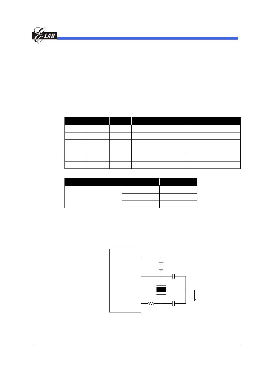
EM78P468N
8-BIT Microcontroller
Product Specification
(V1.2) 03.15.2005
�
35
(This specification is subject to change without further notice)
4.6
lla
4.6
Table 3 Oscillator Modes as defined by FSMD, FMMD1, FMMD0.
Osci tor
.1 Oscillator
Modes
This LSI can operate in the three different oscillator modes from main oscillator (R-OSCI,
OSCO), such as RC oscillator with external resistor and Internal capacitor mode (ERIC);
crystal oscillator mode; and PLL operation mode (R-OSCI connected 0.01
F capacitor to
Ground). User can select one of them by programming FMMD1 and FMMD0 in the
CODE options register. The sub-oscillator can be operated in crystal mode and ERIC
mode. Table 3 below shows how these three modes are defined.
FSMD
FMMD1 FMMD0
Main clock
Sub-clock
0
0
0
RC type (ERIC)
RC type (ERIC)
0
0
1
Crystal type
RC type (ERIC)
0
1
X
PLL type
RC type (ERIC)
1
0
0
RC type (ERIC)
Crystal type
1
0
1
Crystal type
al type
Cryst
1
1
stal type
X
PLL type
Cry
Table 4 Summary of maximum operating speeds
Conditions
VDD
Fxt max.(MHz)
2.3 4
3.0 8
Two clocks
5.0 10
4.6
W
L
req
ine
oscillator. We can
choose RD register to change high oscilla
ncy.
ion b
h
frequency (Fm) and
shown
able:
.2
Phase Lock Loop (PLL Mode)
hen operate on PL mode, the High f
uency determ
d by sub-
tor freque
The relat
etween hig
sub-oscillator is
as below t
Xout
Xin
XTAL
uF
1
R-OSCI
EM78P468N
0.01
C
C2
Circuit for PLL mode
EM78P468N
8-BIT Microcontroller
36
�
Product Specification (V1.2) 03.15.2005
(This specification is subject to change without further notice)
Bit 6~4 (CLK2~0) of RD:
main clock selection bits for PLL mode (code option select)
CLK2
CLK1
CLK0
Main clock
Example Fs=32.768K
0 0 0 Fs*130
4.26
MHz
0 0 1 Fs*65
2.13
MHz
0 1
0
Fs*65/2
1.065
MHz
0 1 1
5
Fs*65/4
32
KHz
1 X
X
8
Fs*244
MHz
4.6.3
/Ceramic Resonators (XTAL)
s shown in
In most applications, the R-OSCI pin and the OSCO pin can be connected with a crystal
or ceramic resonator to generate oscillation. Fig. 10 depicts such circuit. Table 5
provides the recommended values of C1 and C2. Since each resonator has its own
attribute, user should refer to its specification for appropriate values of C1 and C2. RS, a
serial resistor, may be necessary for AT strip cut crystal or low frequency mode.
Crystal Oscillator
This LSI can be driven by an external clock signal through the R-OSCI pin a
Fig.9 below.
EM78P468N
OSCO
R-OSCI
Fig.9 Circuit for External Clock Input
EM78P468N
OSCO
R-OSCI
XTAL
Rs
C1
C2
EM78P468N
Xout
Xin
XTAL
Rs
C2
C1
Fig. 10 Circuit for Crystal/Resonator
Table 5 Capacitor Selection Guide for Crystal Oscillator or Ceramic Resonators
Oscillator source Oscillator Type
Frequency
C1 (pF)
C2 (pF)
455 kHz
100~150
100~150
2.0 MHz
20~40
20~40
Ceramic
Resonators
4.0MHz 10~30 10~30
455KHz 20~40 20~150
1.0MHz 15~30 15~30
2.0MHz 15
15
Main oscillator
Crystal Oscillator
4.0MHz 15
15
Sub-oscillator Crystal
Oscillator
32.768kHz 25
25
EM78P468N
8-BIT Microcontroller
4.6.4
RC Oscillator Mode with Internal Capacitor
If both precision and cost are taken into consideration, This LSI also offers a special
oscillation mode, which is equipped with an internal capacitor and an external resistor
connected to VDD. The internal capacitor functions as temperature compensator. In
order to obtain more accurate frequency, a precise resistor is recommended.
EM78P468N
R-OSCI or Xin
Rext
VDD
Fig. 11 Circuit for Internal C Oscillator Mode
Table 6 RC Oscillator Frequencies
Pin
Rext
Average Fosc 5V, 25
�
C Average Fosc 3V, 25
�
C
51k
2.2221 MHz
2.1972 MHz
100k
1.1345 MHz
1.1203 MHz
R-OSCI
300k 381.36KHz 374.77
KHz
Xin 2.2M
32.768KHz
32.768KHz
Note:
Measured from QFP packages with frequency drift of about
�30%.
Values are provided for design reference only.
Product Specification
(V1.2) 03.15.2005
�
37
(This specification is subject to change without further notice)

EM78P468N
8-BIT Microcontroller
4.7 Power-on Considerations
ted to start operating properly before
steady state. This LSI is equipped with Power On Reset
(POR)
ge of 1.9V to 2.1V. The circuitry eliminates the extra
only if the VDD rises quickly enough (50 ms or
ions, extra devices are still required to assist in
solving p
4.7
t Circuit
e a reset pulse (see Fig.12). The pulse
width (time constant) should be kept long enough to allow VDD to reach minimum
wer supply rise time is slow. Because
5
�A, it is recommended that R should
ed rapidly
esistor, prevents high current discharge or ESD
c
Any microcontroller (as with this LSI) is not warran
the power supply stabilizes in
with detection level ran
external reset circuit but will work well
less). However, under critical applicat
ower-on problems.
.1
External Power-on Rese
This circuit implements an external RC to produc
operation voltage. This circuit is used when the po
the current leakage from the /RESET pin is about
�
not be great than 40K. In this way, the voltage at Pin /RESET is held below 0.2V. The
diode (D) acts as a short circuit at power-down. The capacitor, C, is discharg
and fully. Rin, the current-limited r
(ele trostatic discharge) from flowing into Pin /RESET.
Fig. 12 External Power on Reset Circui
t
.2 Residue-Voltage
Protection
When battery is replaced, device power (VDD) is disconnected but residue-voltage
remains. The residue-voltage may trips below minimum VDD, but above zero. This
condition may cause poor power on reset. Fig.13 and Fig.14 show how to build a
residue-voltage protection circuit
4.7
Fig. 13
Protection
Circuit 1 for the Residue Voltage
38
�
Product Specification (V1.2) 03.15.2005
(This specification is subject to change without further notice)

EM78P468N
8-BIT Microcontroller
Fig. 14 Circuit 2 for the Residue Voltage Protection
errupt
4.8 Int
T
h-pu
erflow interru
w-pu
erflow interrup
riggered or as follows
:
TCC timer overflow interrupt,
F
8-bits down c nter/timer underflow interrupt
If these interrupt source
e sign
w, the RF register will generate "1"
ag to corresponding register if the IOCF0 register is enabled.
flag bit. IOCF0 is the
interrupt mask register. Global interrupt is enabled by ENI instruction and disabled by
o be fetch from address 0003H~0018H according to interrupt source.
n interrupt vector as depicted in
Table 3. Before the interru
the contents of ACC and the R3
regist
r the interrupt service routine is completed,
ACC
rrupt service routine does not allow other
occur while the existing
interrupt service routine is bein
terrupts.
O
t
g inte
ice routine
ted that the next interrupt
servi
e is executed
his LSI has eight interrupt sources as listed below:
TCC overflow interrupt.
External interrupt P5.4/INTO pin
External interrupt P5.5/INT1 pin
Counter 1 underflow interrupt
Counter 2 underflow interrupt
Hig
lse width timer und
pt
Lo
lse width timer und
t
Port 6, Port 8 input status change wake-up
This IC has internal interrupts which are falling edge t
our
ou
s chang
al from high to lo
fl
RF is the interrupt status register. It records the interrupt request in
DISI instruction. When one of the interrupts (when enabled) is generated, it will cause the
next instruction t
With this LSI, each individual interrupt source has its ow
pt subroutine is executed,
er are initially saved by hardware. Afte
and R3 are restored. The existing inte
interrupt service routine to be executed. So if other interrupts
g executed, the hardware will save the later in
nly after he existin
rrupt serv
is comple
ce routin
.
Product Specification
(V1.2) 03.15.2005
�
39
(This specification is subject to change without further notice)

EM78P468N
8-BIT Microcontroller
ACC
R3
STACKACC
40
�
Product Specification (V1.2) 03.15.2005
(This specification is subject to change without further notice)
STACKR3
Interrupt Source
ENI/ DIS
ur
RETI
g. 15. Interrupt Backup Diagram
I
Interrupt Occ
Fi
Table 3 Interrupt Vector
Interrup
ta
Interrupt V tor
ec
t S tus
0003H
TCC overflow interrupt.
0006H
External interrupt P5.4/INT0 pin
0009H
External interrupt P5.5/INT1 pin
000CH
Counter 1 underflow interrupt
000FH
Cou
und
interr
nter 2
erflow
upt
0012H
High-pulse width timer underflow interrupt
0015H
Low-pulse width timer underflow interrupt
0018H
PORT , PORT 8 input status change wake-up
6
4.9 LCD Driver
This LSI can drive LCD of up to 32 segments and 4 commons t t can dr
l of
4*32 dots. LCD blo
is made p of LCD driver, display RAM, egment
ins,
comm
tput pins, and LCD operating power supply pins. This cuit wor
l
mo
mode
d idle mode. Th
ut
the
r f segment; the
number of common and frame frequency are determined by the LCD controller register.
control that uses a subsystem clock to generate the
y ac
s. Th
regis
co
d
regi
CD d
ude
/2 and 1/3), duty (1/2,
1/3, 1/4), and LCD frame frequency co
ol. T
r
l register. The register RB is an LCD RAM data buffer. LCD booster
CD3 drive capability.
ha
ive a tota
ck
u
s
output p
on ou
cir
ks on norma
de, green
an
e LCD d y; bias;
numbe o
The basic structure contains a timing
pr
ing
ffere
and
oper tim
ster for L
for di
river whi
nt duty
displa
s L
cesse
e R9
ter is a mman
ch incl
CD en
ntr
able/disabl
he registe
e, bias (1
RA is an LCD contrast and LCD
RAM address contro
circuit can change operation frequency to improve VLCD2 and VL
The control register is explained as follows.
R9/LCDCR (LCD Control Register)
Bit 7
Bit 6
Bit 5
Bit 4
Bit 3
Bit 2
Bit 1
Bit 0
BS DS1
LCDEN --
LCDTYPE LCDF1 LCDF0
DS0
Bit 7 (B
as select bit, 0/1=>(1/2 bia
S):
LCD bi
s) / (1/3 bias)
Bit 6 ~ 5 (DS1 ~ DS0):
LCD dut
elect
y s
DS1
DS0
LCD Duty
0 0
1/2
duty
0 1
1/3
duty
1 X
1/4
duty

EM78P468N
8-BIT Microcontroller
Product Specification
(V1.2) 03.15.2005
�
41
(This specification is subject to change without further notice)
Bit 4 (LCDEN):
LCD enable bit: 0/1 -> LCD circuit disable/enable
When LCD function is disabled, all common/segment output is set to ground (GND) level
Bit 3:
Not used
Bit 2 (LCDTYPE):
LCD drive waveform type select bit
LCDTYPE = "0": "
A" type waveform
LCDTYPE = "1": "
B" type waveform
Bit 1 ~ 0(LCDF1 ~ LCDF0):
LCD frame frequency control bits
LCD frame frequency (e.g. Fs=32.768KHz)
LCDF1
LCDF0
1/2 duty
1/3 duty
1/4 duty
0 0
Fs/(256*2)=64.0
Fs/(172*3)=63.5
Fs/(128*4)
=64.0
0 1
Fs/(280*2)=58.5
Fs/(188*3)=58.0
Fs/(140*4)
=58.5
1 0
Fs/(304*2)=53.9
Fs/(204*3)=53.5
Fs/(152*4)
=53.9
1 1
Fs/(232*2)=70.6
Fs/(156*3)=70.0
Fs/(116*4)
=70.6
Fs: sub-oscillator frequency
RA/LCD_ADDR (LCD Address)
Bit 7
Bit 6
Bit 5
Bit 4
Bit 3
Bit 2
Bit 1
Bit 0
0 0 0
LCD_A4 LCD_A3 LCD_A2
LCD_A1
LCD_A0
Bit 7 ~ 5:
Not used, fixed to "0"
Bit 4 ~ 0 (LCDA4 ~ LCDA0):
LCD RAM address
RB (LCD data buffer)
RA
(LCD address) Bit 7 ~4
Bit 3
(LCD_D3)
Bit 2
(LCD_D2)
Bit 1
(LCD_D1)
Bit 0
(LCD_D0)
Segmen
t
00H
--
SEG0
01H
--
SEG1
02H
--
SEG2
|
| |
1DH
--
SEG29
1EH
--
SEG30
1FH
--
SEG31
Common
X COM3 COM2 COM1 COM0
RB/LCD_DB (LCD Data Buffer)
Bit 7
Bit 6
Bit 5
Bit 4
Bit 3
Bit 2
Bit 1
Bit 0
--
--
--
--
LCD_D 3 LCD_D 2 LCD_D 1 LCD_D 0
Bit 7 ~ 4:
Not used
Bit 3 ~ 0 (LCD_D3 ~ LCD_D0):
LCD RAM data transfer registers

EM78P468N
8-BIT Microcontroller
42
�
Product Specification (V1.2) 03.15.2005
(This specification is subject to change without further notice)
RD/SBPCR (System, Booster and PLL Control Registers)
Bit 7
Bit 6
Bit 5
Bit 4
Bit 3
Bit 2
Bit 1
Bit 0
-- CLK2 CLK1 CLK0 IDLE BF1 BF0 CPUS
Bit 2 ~ 1 (BF1 ~ 0):
LCD booster frequency select bits
BF1
BF0
Booster frequency
0 0 Fs
0 1
Fs/4
1 0
Fs/8
1 1
Fs/16
The initial setting flowchart for LCD function
IC RESET occur
*Set Port 7 snd Port 8 for general I/O or LCD segment (IOC50)
*it must be set to output port w hen the pin of port 7 and the pin of port 8 for LCD
segemnt (IOC70 and IOC80)
Set LCD Type, duty, bias, LCD frame frequency (R9)
Set LCD Booster Frequency (RD)
Clear all LCD RAM (RA and RB)
Enable LCD function (R9)
Use LCD address and LCD data buffer to implment user's applications. (RA and RB)
END
Fig.16. The Initial Setting Flowchart for LCD Function

EM78P468N
8-BIT Microcontroller
Product Specification
(V1.2) 03.15.2005
�
43
(This specification is subject to change without further notice)
The connecting of boosting circuits for LCD voltage is as below:
VDD
VLCD2(2*VDD/3)
VLCD3(1*VDD/3)
GND
VA
VB
External circuit for 1/3 Bias
VDD
VLCD2(VDD/2)
VLCD3(VDD/2)
GND
VA
VB
External circuit for 1/2 Bias
Fig. 17 The Connection of Charge Bump Circuit (Cext=0.1uf )

EM78P468N
8-BIT Microcontroller
1 frame
COM 0
COM 1
SEG N
SEG N - COM0
VDD
VLCD2,3
GND
VDD
VLCD2,3
GND
VDD
VLCD2,3
GND
VDD
VLCD2,3
GND
-VLCD2,3
-VDD
VDD
VLCD2,3
GND
-VLCD2,3
-VDD
SEG N - COM1
ON
OFF
1/2 bias, 1/2 duty
A type
1 frame
COM 0
COM 1
SEG N
SEG N - COM0
VDD
VLCD2,3
GND
VDD
GND
VDD
GND
VDD
GND
-VDD
VDD
VLCD2,3
GND
-VLCD2,3
-VDD
SEG N - COM1
ON
OFF
1/2 bias, 1/2 duty
B type
VLCD2,3
VLCD2,3
VLCD2,3
-VLCD2,3
Fig. 18 LCD Waveform for 1/2 Bias, 1/2 Duty
1 frame
COM 0
44
�
Product Specification (V1.2) 03.15.2005
(This specification is subject to change without further notice)
1 frame
COM 0
COM 1
COM 2
SEG N
SEG N - COM0
VDD
GND
VDD
GND
VDD
GND
VDD
GND
VDD
GND
-VDD
VDD
GND
-VDD
SEG N - COM1
ON
OFF
1/2 bias, 1/3 duty
A type
-VLCD2,3
VLCD2,3
VLCD2,3
VLCD2,3
VLCD2,3
VLCD2,3
VLCD2,3
-VLCD2,3
COM 1
COM 2
SEG N
SEG N - COM0
VDD
VLCD2,3
GND
VDD
VLCD2,3
GND
VDD
VLCD2,3
GND
VDD
VLCD2,3
GND
VDD
VLCD2,3
GND
-VLCD2,3
-VDD
VDD
VLCD2,3
GND
-VLCD2,3
-VDD
SEG N - COM1
OFF
ON
1/2 bias, 1/3 duty
B type
Fig. 19 LCD Waveform for 1/2 Bias, 1/3 Duty
EM78P468N
8-BIT Microcontroller
1 frame
COM 0
COM 1
COM 2
SEG N
SEG N - COM0
VDD
VLCD2
VLCD3
GND
VDD
VLCD2
VLCD3
GND
VDD
VLCD2
VLCD3
GND
VDD
VLCD2
VLCD3
GND
VDD
VLCD3
GND
-VLCD3
-VDD
SEG N - COM1
ON
OFF
1 frame
COM 0
COM 1
COM 2
SEG N
SEG N - COM0
VDD
VLCD2
VLCD3
GND
VDD
VLCD2
VLCD3
GND
VDD
VLCD2
VLCD3
GND
VDD
VLCD2
VLCD3
GND
VDD
VLCD3
GND
-VLCD3
-VDD
SEG N - COM1
ON
OFF
VDD
VLCD3
GND
-VLCD3
Product Specification
(V1.2) 03.15.2005
�
45
(This specification is subject to change without further notice)
1/3 bias, 1/3 duty
A type
-VDD
1/3 bias, 1/3 duty
B type
VDD
VLCD3
GND
-VLCD3
-VDD
Fig. 20
LCD Waveform for 1/3 Bias, 1/3 Duty
1 frame
COM 0
COM 1
COM 2
SEG N
SEG N -
COM0
VDD
VLCD2
VLCD3
GND
VDD
VLCD2
VLCD3
GND
VDD
VLCD2
VLCD3
GND
VDD
VLCD2
VLCD3
GND
VDD
VLCD3
GND
-VLCD3
-VDD
SEG N -
COM1
ON
OFF
1/3 bias, 1/4
A type
duty
VDD
VLCD3
GND
-VLCD3
-VDD
1 frame
COM 0
COM 1
COM 2
SEG N
SEG N -
COM0
VDD
VLCD2
VLCD3
GND
VDD
VLCD2
VLCD3
GND
VDD
VLCD2
VLCD3
GND
VDD
VLCD2
VLCD3
GND
VDD
VLCD3
GND
-VLCD3
-VDD
SEG N -
COM1
ON
VDD
VLCD3
GND
DD
OFF
1/3 bias, 1/4 duty
B type
-VLCD3
-V
Fig. 21 LCD Waveform r 1/3 Bias, 1/4 Duty
fo

EM78P468N
8-BIT Microcontroller
46
�
Product Specification (V1.2) 03.15.2005
(This specification is subject to change without further notice)
4.10
Infrared Remote Control Application / PWM Waveform
Generate
This LSI can output infrared carrier in a friendly manner or in PWM standard waveform.
The IR and PWM waveform generated functions include an 8-bit down count
timer/counter, high-pulse width timer, low-pulse width timer, and IR control register. The
IR system block diagram is show in Fig.21, The IROUT pin waveform is determined by IR
control register (RE), IOC90 (Counter 1, 2 control register), IOCA0 (high-pulse width
timer, low-pu
unter 2 preset), IOCD0
(high-pulse
w-pulse width timer preset
register). Details on Fcarrier, high ulse time, and low pulse time are explained as
follows
:
If Counter 2
IOC91);
lse width timer control register), IOCC0 (Co
width timer preset register), and IOCE0 (lo
-p
source clock is F (this clock source can set by
T
prescaler
*
))
0
IOCC
(
value
preset
2
counter
of
decimal
+
1
(
*
2
F
=
F
T
carrier
If high-pulse width timer source clock is FT (this clock source can set by IOCA1);
T
time
pulse
high
F
))
0
IOCD
(
value
timer
width
pulse
high
of
decimal
+
1
(
*
prescaler
=
T
If low-pulse width timer source clock is FT (this clock source can set by IOCA1);
T
F
time
pulse
low
))
0
IOCE
(
value
timer
width
pulse
low
of
decimal
+
1
(
*
prescaler
=
T
H/W Modulator Circuit
Pre-scaler
(IOC91)
8 bit dow n counter
Fs
8 bit dow n counter
Pre-scaler
(IOC A 1)
8
A uto-reload buf f er
A uto-reload buf f er
8
8
8 bit dow n counter
8
A uto-reload buf f er
8
IROUT pin
Pre-scaler
(IOCA 1)
IRE
Fcarrier
Fm
LGP
High-Pulse Width Timer
(IOCD0)
Low -Pul
( I
se Width Timer
OCE0)
HF
Counter 2
(IOCC0)
8
RE register
8
8
Fm: main oscillator frequency
;
Fs:
sub-o cillator frequency
. 21 IR/PWM System Block Diagram
s
Fig

EM78P468N
8-BIT Microcontroller
Product Specification
(V1.2) 03.15.2005
�
47
(This specification is subject to change without further notice)
The IROUT output waveform is further explained in the following figures:
Fig. 22
LGP=0, HF=1, the IROUT waveform can modulate Fcarrier waveform when in
low-pulse width time.
Fig. 23
LGP=0, HF=0, the IROUT waveform cannot modulate Fcarrier waveform when
in low-pulse width time. So IROUT waveform is determined by high-pulse time
and low-pulse time. This mode can produce standard PWM waveform
Fig. 24
LGP=0, HF=1, the IROUT waveform can modulate Fcarrier waveform when in
low-pulse width time. When IRE goes from high to low, the output waveform of
IROUT will keep on transmitting till high-pulse width timer interrupt occurs.
Fig. 25
LGP=0, HF=0, the IROUT waveform can not modulate Fcarrier waveform when
in low-pulse width time. So IROUT waveform is determined by high-pulse time
and low-pulse time. This mode can produce standard PWM waveform. When
IRE goes from high to low, the output waveform of IROUT will keep on
transmitting till high-pulse width timer interrupt occurs.
Fig.26
LGP=1, when this bit is set to high level, the high-pulse width timer is ignored.
So IROUT waveform output from low-pulse width timer is established.
Fcarrier
low-pulse width
high-pulse width
IROUT
start
HF
IRE
high-pulse width
low-pulse width
Fig. 22 LGP=0, IROUT Pin Output Waveform
Fcarrier
low-pulse width
high-pulse width
IROUT
start
HF
IRE
high-pulse width
low-pulse width
Fig. 23 LGP=0, IROUT Pin Output Waveform

EM78P468N
8-BIT Microcontroller
Fcarrier
low-pulse width
high-pulse width
IROUT
start
HF
IRE
high-pulse width
low-pulse width
IR disable
Always high-level
Fig. 24 LGP=0, IROUT Pin Output Waveform
Fcarrier
low-pulse width
high-pulse width
IROUT
start
HF
IRE
h-pul
h
hig
se widt
low-pulse width
IR disable
Always high-level
Fig. 25 LGP=0, IROUT Pin Output Waveform
Fcarrier
low-pulse width
Low-pulse width
IROUT
start
HF
IRE
high-pulse width
low-pulse width
IR disable
Always high-level
aveform
Fig. 26 LGP=1, IROUT Pin Output W
48
�
Product Specification (V1.2) 03.15.2005
(This specification is subject to change without further notice)
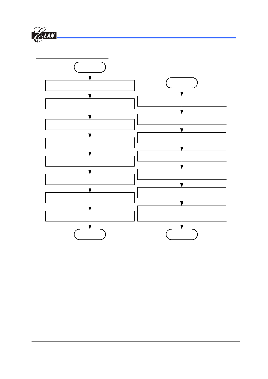
EM78P468N
8-BIT Microcontroller
ion enable flowchart
IR/PWM funct
Product Specification
(V1.2) 03.15.2005
�
49
(This specification is subject to change without further notice)
SET P5.7 to OUTPUT state
(IOC 50)
SET P5.7 for IR/PWM Function Outpu
E)
t Pin
(R
SET Counter 2 clock source and pres
91)
caler
(IOC
SET Count
(IOD0)
, Low
er 2
(IOC0)
, High pulse width timer
pulse width timer
(IOCE0)
preset value
Enable IR
(
HF="1", an
RE)
d IRE="1"
Enable cou
pulde width
nter 2, high pulse width timer and Low
timer
(RC)
SET High pulse width timer, Low pulse width timer
source clock and prescaler
(IOCA1)
Enable HP
Set
IOCF0
WT and LPWT Interrupt
and ENI instruction
STRAT
END
SET P5.7 to OUTPUT state
(IOC 50)
SET P5.7 for IR/PWM F
tput Pin
(RE)
unction Ou
High pulse width timer
(IOD0)
, Low pulse width timer
(IOCE0)
preset value
Enable IR
(RE)
HF="0", and IRE="1"
SET High pulse width timer, Low pulse width timer
source clock and prescaler
(IOCA1)
Enable HPWT and LPWT Interrupt
Set
IOCF0
and ENI instruction
Enable high pulse width timer and Low pulde width
timer
(RC)
STRAT
END
(a) IR application (b) PWM application
Fig. 27 IR/PWM Function Enable Flowchart

EM78P468N
8-BIT Microcontroller
50
�
Product Specification (V1.2) 03.15.2005
(This specification is subject to change without further notice)
4.11 Code Options
word that is not a part of the normal program
e
T
tio
can ot b accessed
l program execu
o
ti
gis
Customer ID
stribution:
o
f c
pt
fo
stomer ID code
.
The EM78P468N has one Code Option
m mory. he op n bits
n
e
during norma
tion.
C de Op on Re
ter and
Register arrangement di
W rd1 o ode o ions is r cu
application
Word 1
Bit12
~Bit 0
Wo
IC prog
rd 0 of Co
ram
de Option
ming
s is for IC function
are the settings for OTP
:
setting. The following
Word 0
Bit12~10
Bit9
Bit8
Bit7
Bit6
Bit5
Bit4
Bit3
Bit2
Bit1
Bit0
1
CYES
H
B FSMD
FMMD
0 HLP PR2 PR1 PR0
LFS ENWDT
1 FMMD
�
Bi
~ 1
ot u
he
its
et
l the time.
Bi
CY
cle select for JMP and CALL
s
ES
":
e struction cycle (J
L) can be execute
ES
":
t
cles (JMP
) can be executed
Bi
HL
ma
b
ci
or select
FS
":
set to select sub-osc
reset occurs.
FS
":
set to select main-osc
hen reset occurs.
Bit 7(ENW
):
o im enable/disab
W
= "
b wa hdog timer.
W
= "1
a
wa
og timer.
Bi
FS
sub
lator type selectio
Bi
(F
1
n
ci tor type
t 12
0:
N
sed.
T se b are s to "1" al
�
t 9 (
ES):
Cy
instruction
CY
= "0
only on in
MP or CAL
d
CY
= "1
two ins ructions cy
and CALL
�
t 8 (
FS):
in or su -os llat
HL
= "0
CPU is
illator when
HL
= "1
CPU is
illator w
�
DTB
Watchd g t er
le bit.
EN DTB
0":
Ena le
tc
EN DTB
":
Dis ble
tchd
�
t 6 (
MD):
-oscil
n.
�
t 5, 4
MMD , 0):
mai Os lla
selection.
FSMD
FMMD1 FMMD0
Main Oscillator Type
Sub Oscillator Type
0
0
0
RC
RC type
type
0
0
1
XT
RC type
AL type
0
1
X
PLL
RC type
type
1 0 0
RC
XTAL
type
type
1
0
1
XTA
XTAL
L type
type
1 1
PLL
XTAL
X
type
type
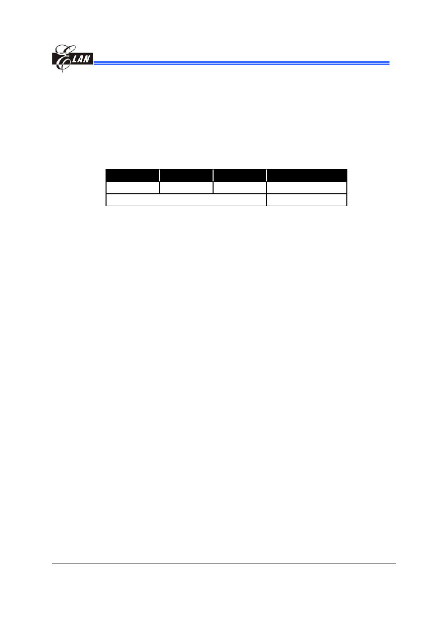
EM78P468N
8-BIT Microcontroller
Product Specification
(V1.2) 03.15.2005
�
51
(This specification is subject to change without further notice)
�
Bit 3 (HLP):
Power consumption selection. If your system usually runs in
de, it
must be set to low power consumption to help support the energy saving issue. We
co
en
low
er cons
ption mod
P
Lo
r consumption mo
P
H
we
nsumption m
it
P
R0
it
R
0
ote
a
xp ned below:
green mo
re mm d that
pow
um
e is slected.
HL = "0":
w powe
de
HL = "1":
igh po
r co
ode
B 2~0 ( R2~P
):
Protect B
P 2~PR are pr
ct bits s e lai
PR2
PR1
PR0
Protect
1 1 1 Disable
Others nable
E
4.12 Instruction Set
Each instruction in the instruction set is a 13-bit word divided into an OP code and one or
more operands. Normally, all instructions are executed within one single instruction cycle
(one instruction consists of 2 oscillator periods), unless the program counter is changed
by instruction "MOV R2,A", "ADD R2,A", or by instructions of arithmetic or logic operation
on R2 (e.g. "SUB R2,A", "BS(C) R2,6", "CLR R2",
). In this case, the execution takes
two instruction cycles.
If for some reasons, the specification of the instruction cycle is not suitable for certain
applications, try modifying the instruction as follows
:
Execute within two instruction cycles the "JMP", "CALL", "RET", "RETL", & "RETI"
instructions, or the conditional skip instructions ("JBS", "JBC", "JZ", "JZA", "DJZ",
"DJZA") which were tested to be true. Also execute within two instruction cycles the
instructions that are written to the program counter.
Additionally, the instruction set offers the following features
:
(1) Every bit of any register can be set, cleared, or tested directly.
(2) The I/O register can be regarded as general register. That is, the same instruction
can operate on I/O register.
The symbol "R" represents a register designator that specifies which one of the registers
(including operational registers and general purpose registers) is to be utilized by the
instruction. "b" represents a bit field designator that selects the value for the bit that is
located in the register "R", and affects operation. "k" represents an 8 or 10-bit constant or
literal value.
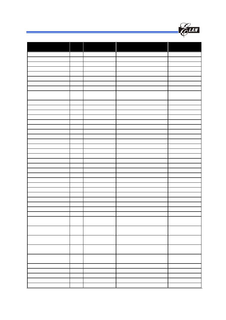
EM78P468N
8-BIT Microcontroller
52
�
Product Specification (V1.2) 03.15.2005
(This specification is subject to change without further notice)
INSTRUCTION BINARY
HEX
MNEMONIC
OPERATION
STATUS
AFFECTED
0 0000 0000 0000 0000 NOP
No
Operation
None
0 0000 0000 0001
0001
DAA
Decimal Adjust A
C
0 0000 0000 0011 0003 SLEP
0
WDT, Stop oscillator
T, P
0 0000 0000 0100 0004 WDTC
0
WDT
T, P
0 0000 0000 rrrr 000r IOW
R
A
IOCR
None <Note1>
0 0000 0001 0000 0010 ENI
Enable
Interrupt
None
0 0000 0001 0001 0011 DISI
Disable
Interrupt
None
0 0000 0001 0010
0012
RET
[Top of Stack]
PC
None
0 0000 0001 0011 0013 RETI
[Top of Stack]
PC,
Enable Interrupt
None
0 0000 0001 rrrr 001r IOR
R
IOCR
A
None <Note1>
0 0000 01rr rrrr 00rr MOV
R,
A
A
R
None
0 0000 1000 0000 0080 CLRA
0
A
Z
0 0000 11rr rrrr 00rr CLR
R
0
R
Z
0 0001 00rr rrrr 01rr SUB
A,
R
R-A
A
Z, C, DC
0 0001 01rr rrrr 01rr SUB
R,
A
R-A
R
Z, C, DC
0 0001 10rr rrrr 01rr DECA
R
R-1
A
Z
0 0001 11rr rrrr 01rr DEC
R
R-1
R
Z
0 0010 00rr rrrr 02rr
OR
A,
R
A
R A
Z
0 0010 01rr rrrr 02rr
OR
R,
A
A
R R
Z
0 0010
10rr
rrrr
02rr
AND
A,
R
A & R
A
Z
0 0010
11rr
rrrr
02rr
AND
R,
A
A & R
R
Z
0 0011 00rr rrrr 03rr XOR
A,
R
A
R A
Z
0 0011 01rr rrrr 03rr XOR
R,
A
A
R R
Z
0 0011
10rr
rrrr
03rr
ADD
A,
R
A + R
A
Z, C, DC
0 0011
11rr
rrrr
03rr
ADD
R,
A
A + R
R
Z, C, DC
0 0100 00rr rrrr 04rr MOV
A,
R
R
A
Z
0 0100 01rr rrrr 04rr MOV
R,
R
R
R
Z
0 0100 10rr rrrr 04rr COMA
R
/R
A
Z
0 0100 11rr rrrr 04rr COM
R
/R
R
Z
0 0101 00rr rrrr
INCA
R
R+1
A
Z
05rr
0 0101 01r
INC
R
R+1
R
Z
r rrrr 05rr
0 0101 10rr rrrr 05rr DJZA
R
R-1
A, skip if zero
None
0 0101 11rr rrrr 05rr
DJZ
R
R-1
R, skip if zero
None
0 0110 00rr rrrr 06rr RRCA
R
R(n)
A(n-1),
R(0)
C, C A(7)
C
0 0110 01rr rrrr 06rr RRC
R
R(n)
R(n-1),
R(0)
C, C R(7)
C
0 0110 10rr rrrr 06rr RLCA
R
R(n)
A(n+1),
R(7)
C, C A(0)
C
0 0110 11rr rrrr 06rr RLC
R
R(n)
R(n+1),
R(7)
C, C R(0)
C
0 0111 00rr rrrr 07rr SWAPA R
R(0-3)
A(4-7),
R(4-7)
A(0-3)
None
0 0111 01rr rrrr 07rr SWAP
R
R(0-3)
R(4-7)
None
0 0111 10rr rrrr 07rr
JZA
R
R+1
A, skip if zero
None
0
0111
11rr rrrr 07rr JZ
R
R+1
R, skip if zero
None
0 100b bbrr rrrr 0xxx
BC
R,
b
0
R(b)
None
0 101b bbrr rrrr 0xxx
BS
R,
b
1
R(b)
None
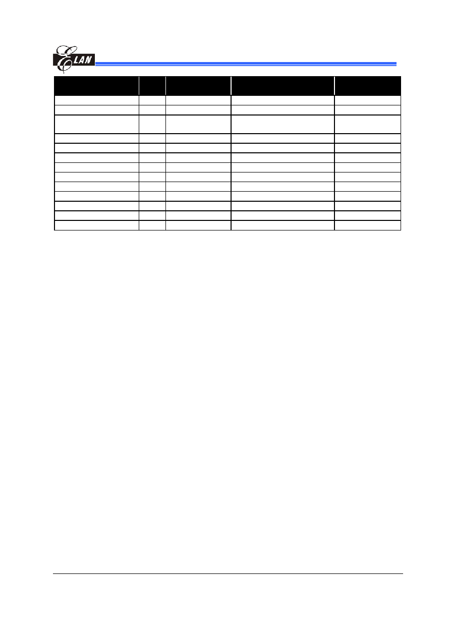
EM78P468N
8-BIT Microcontroller
Product Specification
(V1.2) 03.15.2005
�
53
(This specification is subject to change without further notice)
INSTRUCTION BINARY
HEX
MNEMONIC
OPERATION
STATUS
AFFECTED
0 110b
rrrr
0
C
R,
b
R(b)=0, skip
None
bbrr
xxx
JB
if
0 111b
rrrr
0
S
R,
b
R(b)=1, skip
ne
bbrr
xxx
JB
if
No
1 00kk kkkk kkkk 1kk
ALL
k
PC+1
[SP],
(Page, k)
PC
ne
k C
No
1 01kk kkkk kkkk 1kkk JMP
k
(Page,
k)
PC
None
1 1000 kkkk kkkk 18kk MOV
A,
k
k
A
None
1 1001
19kk
OR
A,
k
A
k A
Z
kkkk kkkk
1 1010 kkkk
kkkk
1Ak
AND
A,
k
A & k
A
Z
k
1 1011 kkkk kkkk 1Bk
XOR
A,
k
A
k A
Z
k
1 1100 kkkk kkkk 1Ckk
RETL
k
k A, [Top of Stack]
PC
ne
No
1 1101 kkkk kkkk 1Dkk SUB
A,
k
k-A
A
, DC
Z, C
1 111
1E8k PAGE
k
k->R5(1:0)
e
0 1000 00kk
Non
1 1110 1001 00kk 1E9K BANK
k
k->R4(7:6)
None
1 1111 kkkk kkkk 1Fkk ADD
A,
k
k+A
A
Z, C, DC
<Note1> This instruction is applicable to IOC50 ~ IOCF0, IOC61 ~ IOCE1
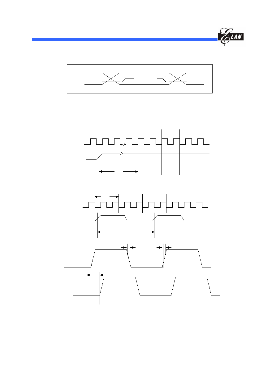
EM78P468N
8-BIT Microcontroller
4.13
Timing Diagram
54
�
Product Specification (V1.2) 03.15.2005
(This specification is subject to change without further notice)
RESET Timing (CLK="0")
CLK
/RESET
NOP
Instruction 1
Executed
Tdrh
TCC Input Timing (CLKS="0")
n
ng : Input is dr
r logic "0".Timing mea
emen
0V
AC Test Input/Output Waveform
CLK
TCC
Ttcc
Ti s
AC Testi
iven at 2.4V for logic "1",and 0.4V fo
sur
ts are
made at 2.
for logic "1",and 0.8V for logic "0".
2.4
0.4
2.0
0.8
TEST POINTS
2.0
0.8
Ttrr
Ttrf
Tiod
90%
90%
Port (n)
*n=0
246
10%
10%
Port (n+1)

EM78P468N
8-BIT Microcontroller
Product Specification
(V1.2) 03.15.2005
�
55
(This specification is subject to change without further notice)
5 ABSOLUTE MAXIMUM RATINGS
Ratin
g
Items
Symbol
Condition
Min.
Max.
Unit
Supply v
GND-0.3
+7.0
V
oltage
VDD
Input vo
V
I
RT 8
-0.3
D+
ltage
PORT 5, PORT 6, PORT 7, PO
GND
VD
0.3
V
Output
O
PORT 5, PORT 6, PORT 7, PORT 8 GND-0.3 VDD+0.3
V
voltage
V
Operati
T
OPR
on temperature
-40
85
S
ge
G
-65
150
tora temperature
T
ST
Power di
P
500
mW
ssipation
D
Operati
32.768K
10M
ng Frequency
Hz

EM78P468N
8-BIT Microcontroller
56
�
Product Specification (V1.2) 03.15.2005
(This specification is subject to change without further notice)
6 ELECTRICAL
CHARACTERISTIC
6.1 DC Electrical Characteristics
(Ta= 25
�C, VDD= 5.0V, GND= 0V)
Symbol
Parameter
Condition
Min.
Typ. Max. Unit
FXT
XTAL: VDD to 5V
Two cycle with two clocks
32.768K
8M
10M
Hz
Fs Sub-oscillator
Two
cycle
with two clocks
32.768
KHz
External R, internal C for
sub-oscillator
R: 300K
, internal capacitance
270 384
500
KHz
ERIC
External R, internal C for
sub-oscillator
R: 2.2M
, internal capacitance
22.9 32.768
42.6
KHz
IIL
Input Leakage Current for
input pins
VIN = VDD, GND
-1
0
1
�A
VIH1
I Input High Threshold
Voltage
(Schmitt trigger)
Ports 5, 6, 7, 8
2.4
V
VIL1
Input High Threshold
Voltage (Schmitt trigger)
Ports 5, 6, 7, 8
0.8
V
VIHT1
Input High Threshold
Voltage (Schmitt trigger)
/RESET 2.4
V
VILT1
Input Low Threshold
Voltage (Schmitt trigger)
/RESET
0.8
V
VIHT2
Input High Threshold
Voltage (Schmitt trigger)
TCC, INT0, INT1
2.4
V
VILT2
Input Low Threshold
Voltage (Schmitt trigger)
TCC, INT0, INT1
0.8
V
IOH1
Output High Voltage
(Ports 5, 6, 7, 8)
VOH = 2.4V, IROCS="0"
-10
mA
IOL1
Output Low Voltage
(Ports 5, 6, 7, 8)
VOL = 0.4V, IROCS="0"
10
mA
IOH1
Output high voltage
(P5.7/IROUT pin)
VOH = 2.4V, IROCS="1"
-20
mA
IOL2
Output Low Voltage
(P5.7/IR OUT pin)
VOL = 0.4V, IROCS="1
20
mA
IPH
Pull-high current
Pull-high active, input pin at GND
-55
-75
-95
�A
IPL
Pull-low current
Pull-low active, input pin at VDD
55
75
95
�A
ISB
Sleep mode current
All input and I/O pins at VDD, output pin
floating, WDT disabled
0.5
1.5
�A
ICC1
Idle mode current
/RESET= 'High', CPU OFF,
sub-oscillator clock (32.768KHz) ON,
output pin floating, LCD enable, no load
14
18
�A
ICC2
Green mode current
/RESET= 'High', CPU ON, used
sub-oscillator clock (32.768KHz),
output pin floating, WDT enabled, LCD
enable
22
30
�A
ICC3 Normal
mode
/RESET= 'High', Fosc=4MHz (Crystal
type, CLKS="0"), output pin floating
2.2
3
mA
ICC4 Normal
mode
/RESET= 'High', Fosc=10MHz (Crystal
type, CLKS="0"), output pin floating
3.1
4
mA

EM78P468N
8-BIT Microcontroller
Product Specification
(V1.2) 03.15.2005
�
57
(This specification is subject to change without further notice)
(Ta= 25
�C, VDD= 3.0V, GND= 0V)
Symbol
Parameter
Condition
Min.
Typ. Max. Unit
FXT
XTAL: VDD to 5V
Two cycle with two clocks
32.768K
8M
10M
Hz
Fs Sub-oscillator
Two
cycle
with two clocks
32.768
KHz
ERIC
External R, internal C for
sub-oscillator
R: 300K
, internal capacitance
270
384
500 KHz
External R, internal C for
sub-oscillator
R: 2.2M
, internal capacitance
22.9
32.768 42.6 KHz
IIL
Input Leakage
input pins
D, GND
-1
0
1
�A
Current for
VIN = VD
VIH1
Input High Th
(Schmitt trigger)
6, 7, 8
1.8
V
reshold Voltage
Ports 5,
VIL1
Input Low Threshold Voltage
(Schmitt trigger)
Ports 5, 6, 7, 8
0.6
V
VIHT1
Input High Threshold Voltage
(Schmitt trigger)
/RESET 1.8
V
VILT1
Input Low Threshold Voltage
(Schmitt trigger)
/RESET
0.6
V
VIHT2
Input High Threshold Voltage
(Schmitt trigger)
TCC, INT0, INT1
1.8
V
VILT2
Input Low Threshold Voltage
(Schmitt trigger)
TCC, INT0, INT1
0.6
V
IOH1
Output High Voltage
(Ports 5, 6, 7, 8)
VOH = 2.4V, IROCS="0"
-1.8
mA
IOL1
Output Low Voltage
(Ports 5, 6, 7, 8)
VOL = 0.4V, IROCS="0"
6
mA
IOH1
Output high voltage
(P5.7/IROUT pin)
VOH = 2.4V, IROCS="1
-3.5
mA
IOL2
Output Low Voltage
(P5.7/IR OU
VOL = 0.4V, IROCS="1
12
mA
T pin)
IPH
Pull-high cu
Pull-high active, input pin at GND
-16
-23
-30
�A
rrent
IPL
Pull-low cur
w active, input pin at VDD
16
23
30
�A
rent
Pull-lo
ISB
Sleep mode current
All input and I/O pins at VDD, output
pin floating, WDT disabled
0.1
1
�A
ICC1
Idle mode current
/RESET= 'High', CPU OFF,
sub-oscillator clock (32.768KHz) ON,
output pin floating, LCD enable, no
load
4
8
�A
ICC2
Green mode current
/RESET= 'High', CPU ON, used
sub-oscillator clock (32.768KHz),
output pin floating, WDT enabled,
LCD enable
10
20
�A
ICC3 Normal
mode
/RESET= 'High', Fosc=4MHz
(Crystal type, CLKS="0"), output pin
floating
0.73
1.2
mA

EM78P468N
8-BIT Microcontroller
58
�
Product Specification (V1.2) 03.15.2005
(This specification is subject to change without further notice)
6.2 AC Electrical Characteristics
(Ta=- 40
�C ~ 85 �C, VDD=5V�5%, GND=0V)
Symbol
Parameter
Conditions
Min
Typ
Max
Unit
Dclk
Input CLK duty cycle
45
50
55
%
Crystal type
100
DC
ns
Tins
Instruction cycle time
(CLKS="0")
RC type
500
DC
ns
Ttcc
TCC input period
(Tins+20)/N*
ns
Tdrh
Device reset hold time
Ta = 25
�C 11.3 16.2 21.6 ms
Trst
/RESET pulse width
Ta = 25
�C 2000
ns
Twdt
Watchdog timer period
Ta = 25
�C 11.3 16.2 21.6 ms
Tset
Input pin setup time
0
ns
Thold
Input pin hold time
20
ns
Tdelay
Output pin delay time
Cload=20pF
50
ns
* N= selected pre-scaler ratio.

EM78P468N
8-BIT Microcontroller
Product Specification
(V1.2) 03.15.2005
�
59
(This specification is subject to change without further notice)
6.3 Device Characteristic
The graphs provided in the following pages were derived based on a limited number of
samples and are shown here for reference only. The device characteristic illustrated
herein are not guaranteed for it accuracy. In some graphs, the data maybe out of the
specified warranted operating range.
Vih/Vil (/RESET pins with schmitt inverter)
0
0.5
1
1.5
2
2.5
2
2.5
3
3.5
4
4.5
5
5.5
Vdd (Volt)
V
i
h/
V
i
l (
V
olt
)
Vih Max. (-40
to +85
)
Vih Typ. (+25
)
Vih Min. (-40
to +85
)
Vil Max. (-40
to +85
)
Vil Typ. (+25
)
Vil Min. (-40
to +85
)
Fig. 28 Vih, Vil of /RESET Pin vs. VDD
Vih/Vil (Port 5, Port 6 All Input pins with schmitt trigger)
0
0.5
1
1.5
2
2.5
2
2.5
3
3.5
4
4.5
5
5.5
Vdd (Volt)
V
i
h V
il
(
V
olt
)
Vih Max. (-40
to +85
)
Vih Typ. (+25
)
Vih Min. (-40
to +85
)
Vil Max. (-40
to +85
)
Vil Typ. (+25
)
Vil Min. (-40
to +85
)
Fig. 29 Vih, Vil of PORT 5 and PORT 6 vs. VDD

EM78P468N
8-BIT Microcontroller
Vih/Vil (Port 7, Port 8 All Input pins with schmitt inverter)
0
0.5
1
1.5
2
2.5
2
2.5
3
3.5
4
4.5
5
5.5
Vdd (Volt)
V
i
h V
il
(
V
olt
)
Vih Max. (-40
to +85
)
Vih Typ. (+25
)
Vih Min. (-40
to +85
)
Vil Max. (-40
to +85
)
Vil Typ. (+25
)
Vil Min. (-40
to +85
)
Fig. 30 Vih, Vil of PORT 7 and PORT 8 vs. VDD
P5.7 Voh/Ioh (VDD=5V, IROCS="0")
-25
-20
-15
-10
-5
0
0
1
2
3
4
5
Voh (Volt)
I
oh (
m
A
)
Typ : +25
Max : -40
Min : +85
P5.7 Voh/Ioh (VDD=3V, IROCS="0")
-10
-8
-6
-4
-2
0
0
0.5
1
1.5
2
2.5
3
Voh (Volt)
Io
h
(
m
A
)
Min : +85
Typ : +25
Max : -40
Fig. 31 Port 5.7 Voh vs. Ioh, [ VDD=3V, 5V, IROCS (Bit 7 of IOC61) =" 0 " ]
60
�
Product Specification (V1.2) 03.15.2005
(This specification is subject to change without further notice)

EM78P468N
8-BIT Microcontroller
P5.7 Voh/Ioh (VDD=5V, IROCS="1")
-50
-40
-30
-20
-10
0
0
1
2
3
4
5
Voh (Volt)
I
oh (
m
A
)
Max : -40
Typ : +25
Min : +85
P5.7 Voh/Ioh (VDD=3V, IROCS="1")
-18
-16
-14
-12
-10
-8
-6
-4
-2
0
0
0.5
1
1.5
2
2.5
3
Voh (Volt)
I
oh (
m
A
)
Typ : +25
Min : +85
Max : -40
Fig. 32 Port 5.7 Voh vs. Ioh, [ VDD=3V, 5V, IROCS (Bit 7 of IOC61) =" 1 " ]
P5.4~6, PORT 6~8 Voh/Ioh (VDD=5V)
-25
-20
-15
-10
-5
0
0
1
2
3
4
5
Voh (Volt)
I
oh (
m
A
)
Typ : +25
Max : -40
Min : +85
P5.4~6, PORT 6~8 Voh/Ioh (VDD=3V)
-10
-8
-6
-4
-2
0
0
0.5
1
1.5
2
2.5
3
Voh (Volt)
I
oh (
m
A
)
Max : -40
Typ : +25
Min : +85
Fig. 33 Port 6, Port 7 and Port 8 Voh vs. Ioh [ VDD=3V, 5V ]
Product Specification
(V1.2) 03.15.2005
�
61
(This specification is subject to change without further notice)
EM78P468N
8-BIT Microcontroller
P5.7 Voh/Ioh (VDD=5V, IROCS="0")
0
10
20
30
40
50
60
70
80
0
1
2
3
4
5
Voh (Volt)
I
oh (
m
A
)
Max : -40
Typ : +25
Min : +85
P5.7 Voh/Ioh (VDD=3V, IROCS="0")
0
5
10
15
20
25
30
35
0
0.5
1
1.5
2
2.5
3
Voh (Volt)
I
oh (
m
A
)
Min : +85
Typ : +25
Max : -40
Fig. 34 Port 5.7 Vol vs. Iol, [ VDD=3V, 5V, IROCS (Bit 7 of IOC61) =" 0 " ]
P5.7 Voh/Ioh (VDD=5V, IROCS="1")
0
20
40
60
80
100
120
140
160
0
1
2
3
4
5
Voh (Volt)
Io
h
(mA
)
Max : -40
Typ : +25
Min : +85
P5.7 Voh/Ioh (VDD=3V, IROCS="1")
0
10
20
30
40
50
60
70
0
0.5
1
1.5
2
2.5
3
Voh (Volt)
Io
h
(
m
A
)
Max : -40
Min : +85
Typ : +25
Fig. 35 Port 5.7 Vol vs. Iol, [ VDD=3V, 5V, IROCS (Bit 7 of IOC61) =" 1 " ]
62
�
Product Specification (V1.2) 03.15.2005
(This specification is subject to change without further notice)
EM78P468N
8-BIT Microcontroller
P5.4~5.6, PORT 6, 7, 8 Voh/Ioh (VDD=5V)
0
10
20
30
40
50
60
70
80
90
0
1
2
3
4
5
Voh (Volt)
I
oh (
m
A
)
Min : +85
Typ : +25
Max : -40
P5.4~5.6, PORT 6, 7, 8 Voh/Ioh (VDD=3V)
0
5
10
15
20
25
30
35
40
0
0.5
1
1.5
2
2.5
3
Voh (Volt)
Io
h
(
m
A
)
Typ : +25
Min : +85
Max : -40
Fig. 36 Port 6, Port 7 and Port 8 Vol vs. Iol [ VDD=3V, 5V ]
Setup time from Power ON Reset
0
5
10
15
20
25
30
35
2
3
4
5
6
VDD (Volt)
s
e
tu
p
ti
m
e
(
m
S
)
Fig. 37 WDT time out period vs. VDD, pre-scaler set to 1:1
Product Specification
(V1.2) 03.15.2005
�
63
(This specification is subject to change without further notice)

EM78P468N
8-BIT Microcontroller
Typical RC OSC Frequency (R-OSCI Pin)
0
0.3
0.6
0.9
1.2
1.5
1.8
2.1
2.4
2
2.5
3
3.5
4
4.5
5
5.5
VDD (Volt)
F
r
e
quenc
y
(
M
H
z
)
R = 51 K
R = 100 K
R = 300 K
Typical RC OSC Frequency (Xin Pin)
30
31
32
33
34
35
2
2.5
3
3.5
4
4.5
5
5.5
VDD (Volt)
F
r
equenc
y
(
K
H
z
)
R = 2.2 M
Fig. 38 Typical ERIC OSC Frequency vs. VDD (Temperature at 25
)
Fig. 39 Typical ERIC OSC Frequency vs. Temperature (R-OSCI Pin)
64
�
Product Specification (V1.2) 03.15.2005
(This specification is subject to change without further notice)

EM78P468N
8-BIT Microcontroller
Fig. 40 Typical ERIC OSC Frequency vs. Temperature (Xin Pin)
Four conditions exist with the Operating Current ICC1 to ICC4. These conditions are as
follows:
ISB (sleep mode):
Fm and Fs is stop, all function off.
ICC1 (idle mode):
Fm Stop and Fs=32K Hz, 2 clocks, CPU off, LCD enable and WDT
Enable.
ICC2 (green mode):
Fm Stop and Fs=32K Hz, 2 clocks, CPU running on Fs frequency,
LCD enable and WDT Enable
ICC3 (normal mode):
Fm=4M Hz and Fs=32K Hz, 2 clocks, CPU running on Fm
frequency, LCD enable and WDT Enable
Product Specification
(V1.2) 03.15.2005
�
65
(This specification is subject to change without further notice)
EM78P468N
8-BIT Microcontroller
Typical ICC3 vs. Temerature
0
0.4
0.8
1.2
1.6
2
-40
-20
0
25
50
70
85
Temperature ()
Cu
r
r
e
n
t
(
m
A
)
VDD=5V
VDD=3V
Fig. 40 Typical power consumption on normal mode operation (Fm=4MHz)
Maximum ICC3 vs. Temerature
0
0.4
0.8
1.2
1.6
2
2.4
2.8
-40
-20
0
25
50
70
85
Temperature ()
C
u
rre
n
t
(m
A
)
VDD=5V
VDD=3V
Fig. 41 Maximum power consumption on normal mode operation (Fm=4MHz
)
66
�
Product Specification (V1.2) 03.15.2005
(This specification is subject to change without further notice)
EM78P468N
8-BIT Microcontroller
Typical ICC2 vs. Temerature
0
5
10
15
20
25
30
-40
-20
0
25
50
70
85
Temperature ()
Cu
r
r
e
n
t
(
u
A
)
VDD=5V
VDD=3V
Fig. 42 Typical power consumption on green mode operation
Maximum ICC2 vs. Temerature
0
5
10
15
20
25
30
35
-40
-20
0
25
50
70
85
Temperature ()
Cu
r
r
e
n
t
(
u
A
)
VDD=5V
VDD=3V
Fig. 43 Maximum power consumption on green mode operation
Product Specification
(V1.2) 03.15.2005
�
67
(This specification is subject to change without further notice)
EM78P468N
8-BIT Microcontroller
Typical ICC1 vs. Temerature
0
5
10
15
20
-40
-20
0
25
50
70
85
Temperature ()
Cu
r
r
e
n
t
(
u
A
)
VDD=5V
VDD=3V
Fig. 44 Typical power consumption on idle mode operation
Maximum ICC1 vs. Temerature
0
5
10
15
20
25
-40
-20
0
25
50
70
85
Temperature ()
Cu
r
r
e
n
t
(
u
A
)
VDD=5V
VDD=3V
Fig. 45 Maximum power consumption on idle mode operation
68
�
Product Specification (V1.2) 03.15.2005
(This specification is subject to change without further notice)

EM78P468N
8-BIT Microcontroller
Typical ISB vs. Temerature
0
0.2
0.4
0.6
0.8
1
-40
-20
0
25
50
70
85
Temperature ()
Cu
r
r
e
n
t
(
u
A
)
VDD=5V
VDD=3V
Fig. 46 Typical power consumption on sleep mode operation
Maximun ISB vs. Temerature
0
0.3
0.6
0.9
1.2
-40
-20
0
25
50
70
85
Temperature ()
Cu
r
r
e
n
t
(
u
A
)
VDD=5V
VDD=3V
Fig. 47 Maximum power consumption on sleep mode operation
Product Specification
(V1.2) 03.15.2005
�
69
(This specification is subject to change without further notice)
EM78P468N
8-BIT Microcontroller
Fig. 48 Operating voltage under temperature range of 0
to 70
Fig. 49 Operating voltage under temperature range of -40
to +85
70
�
Product Specification (V1.2) 03.15.2005
(This specification is subject to change without further notice)

EM78P468N
8-BIT Microcontroller
Product Specification
(V1.2) 03.15.2005
�
71
(This specification is subject to change without further notice)
7 APPLICATION
CIRCUIT
LCD PANEL
COM0
|
COM3
SEG0
|
SEG31
5
1
6
2
7
3
8
4
D
9
E
A
F
B
G
C
P6.0
P6.1
P6.2
P6.3
P6.4
P6.5
P6.6
P6.7
VDD
IROUT
EM
78P468N
Fig. 50 IROUT control external BJT circuit to drive infrared emitting diodes
LCD PANEL
COM0
|
COM3
SEG0
|
SEG31
5
1
6
2
7
3
8
4
D
9
E
A
F
B
G
C
P6.0
P6.1
P6.2
P6.3
P6.4
P6.5
P6.6
P6.7
VDD
IROUT
EM
78P468N
Fig. 51 IROUT direct drive infrared emitting diodes

EM78P468N
8-BIT Microcontroller
72
�
Product Specification (V1.2) 03.15.2005
(This specification is subject to change without further notice)
APPENDIX A:
A.1 Package Types:
A.2 Package Information:
QFP � 64
TITLE:
QFP-64 L(14*20 MM) FOOTPRINT 5.0mm
PACKAGE OUTLINE DIMENSION
Unit : mm
Scale: Free
File :
QFP 64L
Material:
Edtion: A
Sheet:1 of 1
A1
Symbal Min Normal Max
A
3.40
A1
0.25
A2
2.55
2.72
3.05
D
D1
E
E1
0�
3. 5
7�
c 0.11
0.15
0.23
L
1.15
1.3
1.45
L1
b
0.35
0. 4
0.50
e
2.50 REF
1.00 BSC
14.00 BASIC
25.00 BASIC
20.00 BASIC
19.00 BASIC
Name
Package Type
Pin Count
Package Body Size
EM78P468NH Dice
59
EM78P468NQ
QFP
64
14 mm * 20 mm
EM78P468NAQ
LQFP
64
7 mm * 7 mm
EM78P468NBQ
LQFP
44
10 mm * 10 mm
EM78P468NCQ
QFP
44
10 mm * 10 mm

EM78P468N
8-BIT Microcontroller
Product Specification
(V1.2) 03.15.2005
�
73
(This specification is subject to change without further notice)
LQFP � 64
TITLE:
LQFP 64L ( 7*7 MM ) FOOTPRINT 2.0 mm
PACKAGE OUTLINE DIMENSION
Unit : mm
Scale: Free
File :
LQFP 64L
Material:
Edtion: A
Sheet:1 of 1
L1
L
A1
A2
A
b
D
E
1
64
e
D1
E1
DETAIL " A "
DETAIL " B "
b
b1
c1
c
Symbal Min Normal Max
A
-
-
1.60
A1
0.05
-
0.15
A2
1.35
1.40
1.45
D
8.90
9.00
9.10
D1
6.90
7.00
7.10
E
8.90
9.00
9.10
E1
6.900
7.00
7.100
e
c
0.09
-
0.20
c1
0.09
-
0.16
b
0.13
0.18
0.23
b1
0.13
0.16
0.19
L
0.45
0.60
0.75
L1
0�
3.5�
7�
1.00 REF.
0.4 BSC
LQFP � 44
TITLE:
LQFP-44L(10*10 MM) FOOTPRINT 2.0mm
PACKAGE OUTLINE DIMENSION
Unit : mm
Scale: Free
File :
LQFP44
Material:
Edtion: A
Sheet:1 of 1
c
Symbal
A
A1
A2
b
c
E1
E
L
L1
e
Min Normal Max
1.600
0.050
0.150
1.350
1.400
1.450
0.300
0.370
0.450
0.090
0.200
0.450
0.600
0.750
0.8(BASIC)
0
3.5
7
10.00 BASIC
1.0(BASIC)
12.00 BASIC

EM78P468N
8-BIT Microcontroller
74
�
Product Specification (V1.2) 03.15.2005
(This specification is subject to change without further notice)
QFP � 44
TITLE:
QFP-44L(10*10 MM) FOOTPRINT 3.2mm
PACKAGE OUTLINE DIMENSION
Unit : mm
Scale: Free
File :
QFP44
Material:
Edtion: A
Sheet:1 of 1
c
Symbal
A
A1
A2
b
c
E1
E
L
L1
e
Min Normal Max
2.70
0.15
0.50
1.80
2.00
2.20
13.00
13.20
13.40
9.90
10.00
10.10
0.73
0.88
1.03
1.50
1.60
1.70
0
7
0.30(TYP)
0.15(TYP)
0.80(TYP)

EM78P468N
8-BIT Microcontroller
Product Specification
(V1.2) 03.15.2005
�
75
(This specification is subject to change without further notice)
APPENDIX B: EM78P468N Program Pin List
It uses DWRT to program EM78P468N IC's. The connector of DWTR select by CON4
(EM78P451), and the software is selected by EM78P468N.
Program Pin Name
IC Pin Name
L/QFP-64
Pin Number
L/QFP-44
Pin Number
VPP /RESET 25
14
ACLK P54/INT0 32
21
DINCLK P55/INT1
33
22
DATAIN P56/TCC
34
23
/PGMB P60 38
25
/OEB P61 39 26
VDD VDD 29 18
GND GND 26 15
Wiring diagram is for ELAN DWTR

EM78P468N
8-BIT Microcontroller
76
�
Product Specification (V1.2) 03.15.2005
(This specification is subject to change without further notice)
APPENDIX C:
C.1 ICE 468XA Oscillator circuit (JP 5)
Mode1:
Main oscillator: Crystal mode, Sub oscillator: Crystal mode
Sub oscillator
Main oscillator
GND
GND
R-OSCI
OSCO
GND
GND
Xin
Xout
Xin
R-OSCI
VDD
VDD
Crystal
Crystal
JP 5
Mode2:
Main oscillator: PLL mode, Sub oscillator: Crystal mode
Sub oscillator
Main oscillator
GND
GND
R-OSCI
OSCO
GND
GND
Xin
Xout
Xin
R-OSCI
VDD
VDD
PLL
Crystal
JP 5
Mode3:
Main oscillator: RC mode, Sub oscillator: Crystal
Sub oscillator
Main oscillator
GND
GND
R-OSCI
OSCO
GND
GND
Xin
Xout
Xin
R-OSCI
VDD
VDD
Crystal
JP 5
RC

EM78P468N
8-BIT Microcontroller
Product Specification
(V1.2) 03.15.2005
�
77
(This specification is subject to change without further notice)
Mode4:
Main oscillator: Crystal mode, Sub oscillator: RC mode
Sub oscillator
Main oscillator
GND
GND
R-OSCI
OSCO
GND
GND
Xin
Xout
Xin
R-OSCI
VDD
VDD
Crystal
RC
JP 5
Mode5:
Main oscillator: PLL mode, Sub oscillator: RC mode
Sub oscillator
Main oscillator
GND
GND
R-OSCI
OSCO
GND
GND
Xin
Xout
Xin
R-OSCI
VDD
VDD
PLL
JP 5
RC
Mode6:
Main oscillator: RC mode, Sub oscillator: RC mode
Sub oscillator
Main oscillator
GND
GND
R-OSCI
OSCO
GND
GND
Xin
Xout
Xin
R-OSCI
VDD
VDD
JP 5
RC
RC

EM78P468N
8-BIT Microcontroller
78
�
Product Specification (V1.2) 03.15.2005
(This specification is subject to change without further notice)
C.2 ICE 468XA output pin assignment (JP 3)
1
2
3
VB
5
7
9 11 13 15 17 19 21 23 25 27 29 31 33 35 37 39 41 43 45 47 49 51 53 55 57 59
4
6
8 10 12 14 16 18 20 22 24 26 28 30 32 34 36 38 40 42 44 46 48 50 52 54 56 58 60
VL
C
D
2
/
R
E
SET
R-
O
S
CI
VD
D
X
out
P
5
.5
/IN
T
1
SE
G
3
0
/
P
8
.
6
P
5
.7
/IR
OU
T
P6
.
1
P6
.
3
P6
.
5
P6
.
7
SE
G
2
8
/
P
8
.
4
SE
G
2
6
/
P
8
.
2
SE
G
2
4
/
P
8
.
0
SE
G
2
2
/
P
7
.
6
SE
G
2
0
/
P
7
.
4
SE
G
1
8
/
P
7
.
2
SE
G
1
6
/
P
7
.
0
SE
G
1
4
SE
G
1
2
SE
G
1
0
SE
G
8
SE
G
6
SE
G
4
SE
G
2
SE
G
0
CO
M
2
CO
M
0
VA
V
L
CD3
GN
D
OS
C
O
Xi
n
P
5
.4
/IN
T
0
P5
.
6
/
T
C
C
P6
.
0
P6
.
2
P6
.
4
P6
.
6
SE
G
3
1
/
P8
.
7
SE
G
2
9
/
P8
.
5
SE
G
2
7
/
P8
.
3
SE
G
2
5
/
P8
.
1
SE
G
2
3
/
P7
.
7
SE
G
2
1
/
P7
.
5
SE
G
1
9
/
P7
.
3
SE
G
1
7
/
P7
.
1
SE
G
1
5
SE
G
1
3
SE
G
1
1
SE
G
9
SE
G
7
SE
G
5
SE
G
3
SE
G
1
CO
M
3
CO
M
1
JP 3
T