 | ÐлекÑÑоннÑй компоненÑ: EM78P568 | СкаÑаÑÑ:  PDF PDF  ZIP ZIP |
Äîêóìåíòàöèÿ è îïèñàíèÿ www.docs.chipfind.ru

ELAN MICROELECTRONICS CORP.
No. 12, Innovation 1
st
RD., Science-Based Industrial Park
Hsin Chu City, Taiwan
TEL: (03) 5639977
FAX: (03) 5630118 (Elan SA2)
EM78P568
8-BIT OTP MICRO-CONTROLLER
Version 4.7
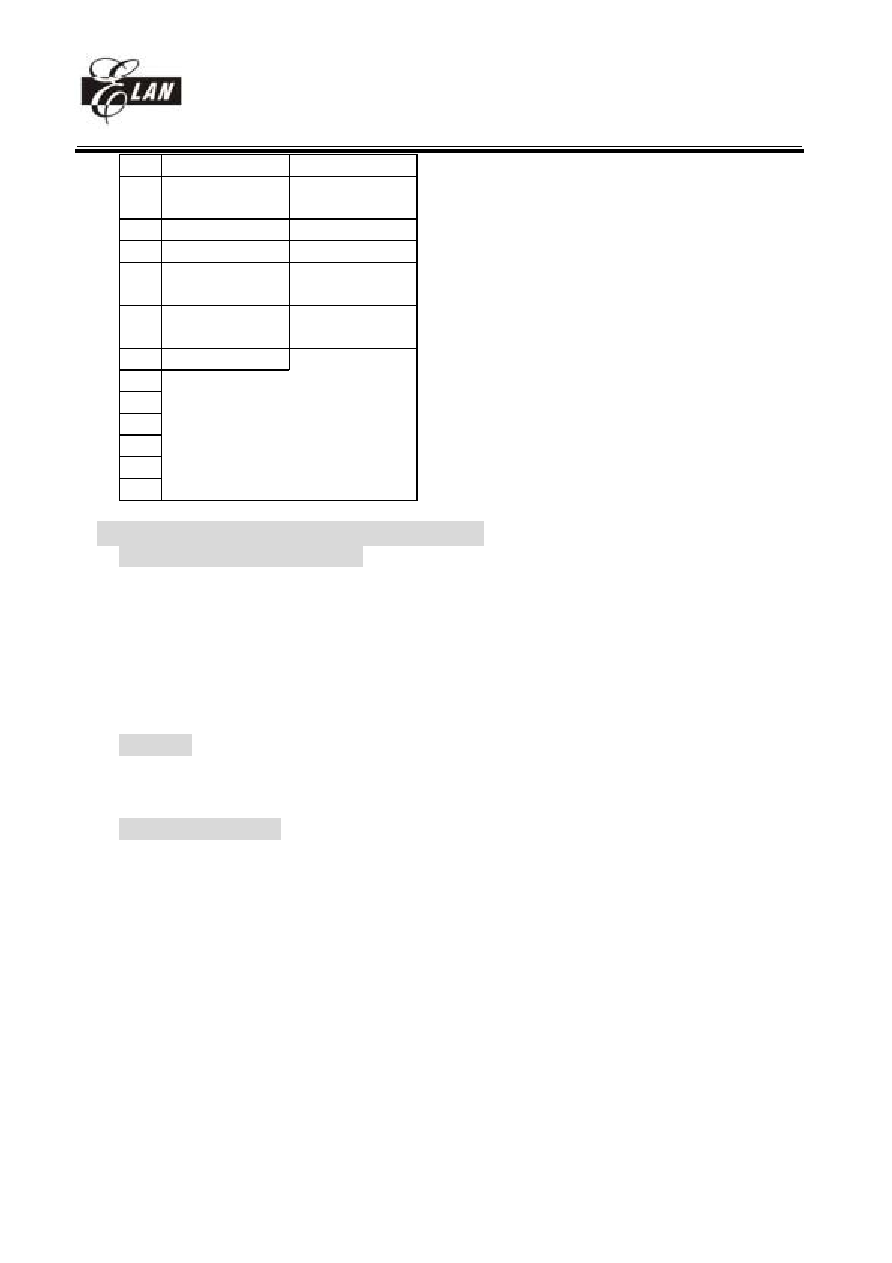
Version History
Specification Revision History
Version Content
EM78P568
1.0 Initial
version
2002/01/11
1.1
Change pin configuration
2002/04/08
1.2
Change pin configuration
2002/05/09
1.3
1.Update initial value of IOCA PAGE1 bit 3 from "x" to "0"
2.Change pin configuration on SEG20 ~ SEG28 pins locations
2002/05/16
2.0
1. Change R3 PAGE setting registers
2. Update register configuration and initial value tables
3. Add LCD waveform option bit. The new option : switch over LCD bias V1
and V2 for segments but bias remain unchanged for commons.
4.Modified pin configuration
5.Modified register setting
2002/06/12
2.1
Update error description and drawing
2002/06/19
2.2
Revise Fig.4 and Fig.5
2002/06/25
2.3
Change pin configuration
2002/08/30
2.4
Correct most of Figure #
2002/09/17
2.5
1. Change P73 interrupt setting from INT2 to INT3
2.Update pin configuration and pin description
3.Update relative RF, IOCF register bit description
2002/09/23
3.0
1.Add item 1 ~ 3 in the user application note (see user application note)
2.Clarify "not existent", "unknown"or "undefined bits" descriptions.
3.Add LCD Type0 and Type1 waveform
4.Revised ROM size from 32kx13 to 16kx13 in the R2 description
2002/10/16
3.1
Change R3's C,DC and Z flag status from "R" to "R/W"
2002/10/29
3.2
Fix bug in the application note
2002/1031
3.3
1.Revise pin name of pin37,38 in the pin configuration figure
2.Revise description of IOC6 PAGE1 bit 0 ~ bit 1.
3.Add new application note on IOC6 PAGE1 bit 0 ~ bit 1.
2002/11/04
3.4
Revise test condition of electrical characteristic 2002/11/07
3.5
1.Update operating voltage of Comparator, DAC and CTCSS block in the
feature description
2.Add DC voltage characteristic for 2.5VREF.
3.Revise sleep current max value from 8uA to 5uA.
4.add description in user application note
2002/11/22
3.6
1.Add DC characteristic under VDD=3V for 2.5VREF
2.Update description in user application note
2002/11/26
3.7
1.Update DC characteristic
2.Add effective VDD reference spec
3.Remove /POVD function
4.Update user application note
2002/11/29
3.8
1.Revised waveform of LCD 1/4 duty for Type 1
2.Revise CTCSS block figure
2003/01/15
3.9
1.Update DC characteristic for 2.5Vref spec and I/O port sink current spec.
2.Change OTP programming pin from P7(4~7) to P6(2~5) as following
DINCK : change from P77 to P65
ACLK : change from p76 to P64
PGMB change from P75 to P63
OEB : change from P74 to P62
2003/02/12
4.0
1 Revise description in operating current for analog circuit
2.Revise dB to dBm on level for CTCSS tone to MTX
2003/10/24
4.1
1. Update application circuit Fig.23
2. Add VII.10 section
2004/07/15
4.5
1. Update VII.9, VII.10 sections
2. Add VII.11, VII.12, VII.13 sections
2004/07/15

EM78P568
8-bit OTP Micro-controller
__________________________________________________________________________________________________________________________________________________________________
* This specification are subject to be changed without notice.
1
01/31/2004 V4.7
3. Update Fig.4, 5 ,7, 10, 12, 14, 16, 18, 19, 20, 21
4. Add Fig.15, 22, 23
5. Make some figures with color
6. Add OSC and reset timing characteristic in page 52
4.6
1. Add AC characteristic of AURX and MTX driving capacity for CTCSS
block in page 52
2. Add AC characteristic of AURX and MTX output loading impedance for
CTCSS block in page 52
2004/12/24
4.7
1. Update the title of VII.10 (3) and (4)
2. Revise Fig.23 bit location error
3. Update AC characteristics spec for CTCSS block
4. Add note on AC characteristics spec for CTCSS block item "Zero crossing
threshold"
5. Add VII.10.2 and more descriptions in VII.10 section
2005/01/31
User Application Note
(Before using this chip, take a look at the following description note, it includes important messages.)
1. There are some undefined bits in the registers. The values in these bits are unpredicted. These
bits are not allowed to use. We use the symbol "-" in the spec to recognize them.
2. You will see some names for the register bits definitions. Some name will be appear very
frequently in the whole spec. The following describes the meaning for the register's definitions
such as bit type, bit name, bit number and so on.
7
6
5
4
3
2
1
0
RAB7
RAB6
BAB5
RAB4
RAB2
RAB0
R/W -0
R/W -0
R-1
R/W -1
R
R/W
Bit type
Bit name
Bit number
read/write
(default value=0)
read/write
(default value=1)
read only
(w/o default value)
read/write
(w/o default value)
PAGE0
RA
Register name and its page
-
RAB1
(undefined) not allowed to use
R-0
read only
(default value=0)
read only
(default value=1)
3. Let "IOCE PAGE0 Bit 4 ~ Bit 7" remain these values to "0"othwise it will generate unpredicted
interrupts.
4. Let "IOCC PAGE1 Bit 0" remain its value to "0" unchanged otherwise Comparator and CTCSS
function will fail.
5. Let IOC6 PAGE1 bit 0 ~ Bit 1 remain these values to "0" unchanged if PORT60,61 are used.
6. Please set RA PAGE2 bit 7 to "1" to get better LCD display performance while LCD driver is
used.
7. The difference between EM78568 and EM78P568.
Function
Item EM78568
EM78P568
Data RAM
0.5k x 8
1k x 8
I/O
PC0
PC0 ~ PC7
PB0 ~ PB7
LCD driver
SEG0 ~ SEG19
SEG0 ~ SEG31
Package
100-pin QFP,63-pin die
100-Pin QPF, 78-pin die
DC characteristic
Parameter Symbol
Condition
Min Typ
Max
Unit
Internal 2.5V ref.. 2.5VREF VDD=5V, 25 deg for EM78568 2.32 2.46
2.58 V
Voltage
VDD=5V, 25 deg for EM78P568 2.14 2.32 2.44 V
VDD=3V, 25 deg for EM78568 2.22 2.36
2.48 V
VDD=3V, 25 deg for EM78P568 2.04 2.25 2.36 V

8. In the feature description CPU operating voltage 2.2 ~ 5.5V, the minimum operating voltage 2.2V
is under maximum main clock = 3.5826MHz
EM78P568
8-bit OTP Micro-controller
__________________________________________________________________________________________________________________________________________________________________
* This specification are subject to be changed without notice.
1
01/31/2004 V4.7
I. General Description
The EM78P568 is an 8-bit RISC type microprocessor with low power, high speed CMOS technology. There are
16Kx13 bits Electrical One Time Programmable Read Only Memory (OTP-ROM) within it. It provides security bits and
some One time programmable Option bits to protect the OTP memory code from any external access as well as to meet
user's options.
This integrated single chip has an on_chip watchdog timer (WDT), program OTP-ROM, data RAM, LCD driver,
programmable real time clock/counter, internal interrupt, power down mode, 8-bit D/A, 5-bit Comparator, DAC tone
generator, CTCSS analog circuit, programming dual tone generator and tri-state I/O.
II. Feature
CPU
·
Operating voltage : 2.2V5.5V
·
16k x 13 on chip Electrical One Time Programmable Read Only Memory (OTP-ROM)
·
1k x 8 on chip data RAM
·
Up to 51 bi-directional tri-state I/O ports
·
16 level stack for subroutine nesting
·
8-bit real time clock/counter (TCC)
·
two 8-bit counters : COUNTER1 and COUNTER2
·
On-chip watchdog timer (WDT)
·
99.9 single instruction cycle commands
·
Four modes (Main clock can be programmed from 447.829k to 17.913MHz generated by internal PLL)
Mode
CPU status
Main clock
32.768kHz clock status
Sleep mode
Turn off
Turn off
Turn off
Idle mode
Turn off
Turn off
Turn on
Green mode
Turn on
Turn off
Turn on
Normal mode
Turn on
Turn on
Turn on
·
Input port interrupt function
·
8 interrupt source, 4 external, 8 internal
·
Dual clocks operation (Internal PLL main clock , External 32.768KHz)
PROGRAMMING TONE GENERATORS
·
Operating voltage : 2.2V5.5V
·
Programming Tone1 and Tone2 dual tone generators
·
11-bit programming Tone1 generators
·
8-bit programming Tone2 generator
COMPARATOR
·
Operating : 2.7V ~ 5.5V
·
3-channel input
·
5-bit comparison reference level setting
·
Internal (2.5V or VDD) or external reference level
DAC
·
Operating : 2.7V5.5V
·
8-bit R-2R D/A converter
·
8-bit programmable tone output
·
Easy to direct access as programmable CTCSS tone output by DAC tone generator
·
Internal (VDD or 2.5V) reference

EM78P568
8-bit OTP Micro-controller
__________________________________________________________________________________________________________________________________________________________________
* This specification are subject to be changed without notice.
2
01/31/2004 V4.7
CTCSS block
·
Operating voltage : 2.7V5.5V
·
Microphone amplifier (can be used as general OP Amp)
·
Microphone mute function
·
RX input OP
·
Audio BPF (300Hz ~ 3400Hz)
·
Sub-audio LPF (60Hz ~ 253Hz) for CTCSS tone detection
·
Zero-crossing for detected CTCSS tone frequency output
·
CTCSS Tx modulation summing Amp
LCD
·
Common driver pins : 4
·
Segment driver pins : 32
·
1/3 bias
·
1/4 duty, 1/2 duty
·
16 Level LCD contrast control by software
PACKAGE
·
100-pin QFP (EM78P568Q)
78-pin die (EM78P568H)
III. Application
FRS (Family Radio Systems) ,other wireless and portable products,

EM78P568
8-bit OTP Micro-controller
__________________________________________________________________________________________________________________________________________________________________
* This specification are subject to be changed without notice.
3
01/31/2004 V4.7
IV. Pin Configuration
NC
NC
NC
NC
NC
NC
1
2
3
4
5
6
7
8
9
10
11
12
13
14
15
16
17
18
21
22
24
25
27
28
29
30
50
49
48
47
46
45
44
43
42
41
40
39
38
37
36
35
75
74
73
70
69
68
67
66
65
64
63
62
61
60
59
58
57
56
55
54
53
52
51
20
26
SEG21/PB7
33
34
19
23
31
32
CM
P
1
/
P
6
2
P61
P60
P87
72
71
SEG
13/
P97
SEG
12/
P57
SEG
11/
P56
SEG
10/
P55
82
83
84
85
86
87
88
89
90
91
92
93
94
95
96
97
98
99
100
81
SEG
14/
P96
SEG
15/
P95
SEG23/PB5
SEG24/PB4
SEG25/PB3
SEG26/PB2
SEG27/PB1
SEG28/PB0
SEG29/PC7
SEG30/PC6
SEG31/PC5
PC4
PC3
PC2
PC1
PC0
SEG22/PB6
SEG
1
SEG
9
SEG
8
SEG
7
SEG
6
SEG
5
SEG
4
SEG
3
SEG
2
D
AO/
P
6
7
MT
X
/
P
6
6
AU
R
X
/
P
6
5
CM
P
3
/
P
6
4
CM
P
2
/
P
6
3
P86
P85
XI
N
X
OUT
VS
S
P84
P83
P82
NC
NC
NC
NC
NC
NC
80
79
78
NC
77
76
NC
NC
NC
NC
P77
P76
P75
P74
INT3/P73
INT2/P72
INT1/P71
INT0/P70
VDD
P81
P80
AVDD
RXO
RXI
NC
NC
PLLC
MICI
MICO
TONE
NC
NC
NC
/R
E
S
E
T
AVSS
SEG
16/
P94
SEG
18/
P92
SEG
19/
P91
SEG
20/
P90
SEG
17/
P93
SEG0
COM3
COM2
COM1
COM0
100-pin QFP or 78-pin die
Fig.1 Pin assignment
EM78P568
8-bit OTP Micro-controller
__________________________________________________________________________________________________________________________________________________________________
* This specification are subject to be changed without notice.
4
01/31/2004 V4.7
OTP PIN NAME
MASK ROM PIN NAME
P.S.
VDD VDD,AVDD
VPP /RESET
DINCK P65
ACLK P64
PGMB P63
OEB P62
DATA P73
GND VSS,AVSS
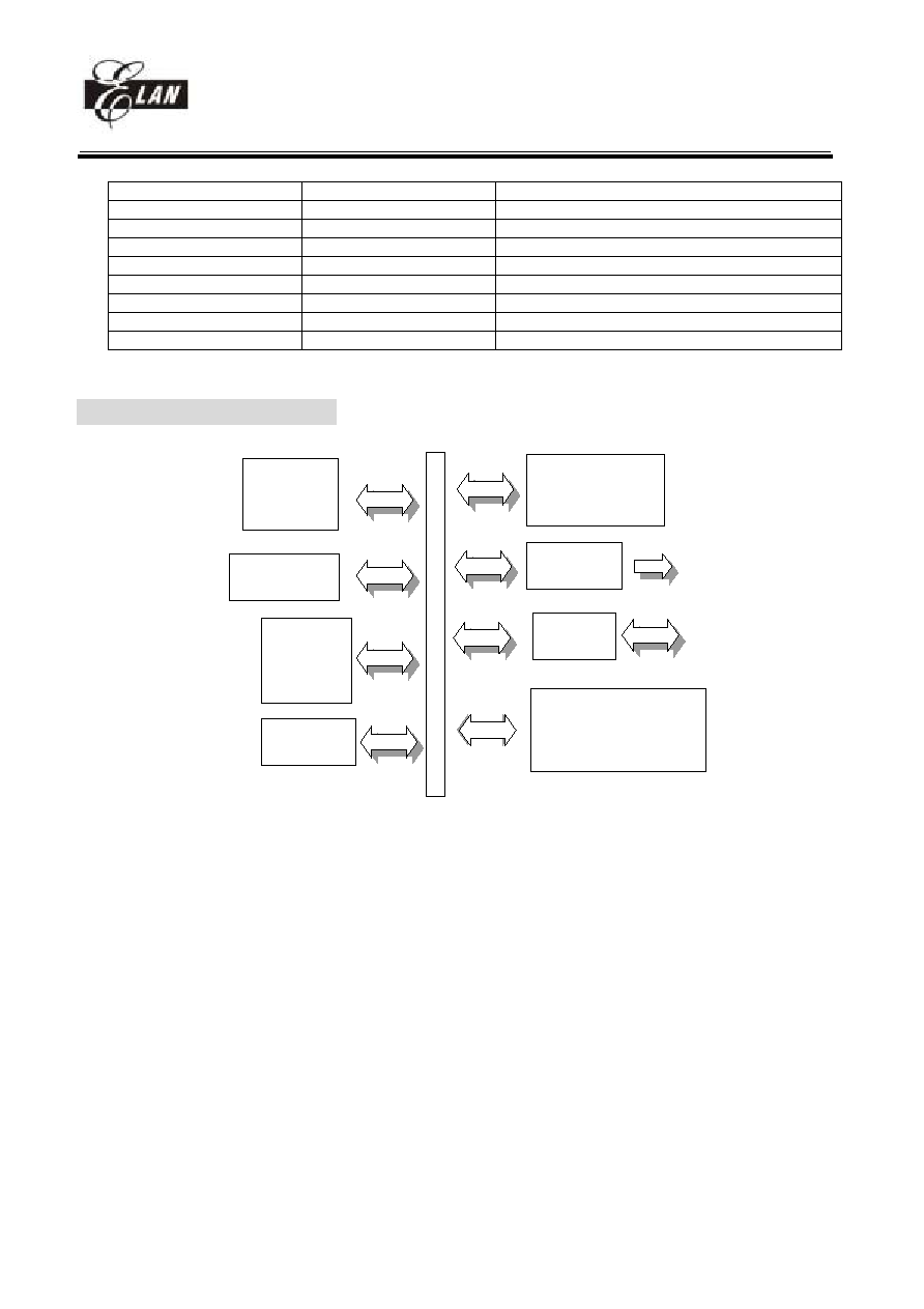
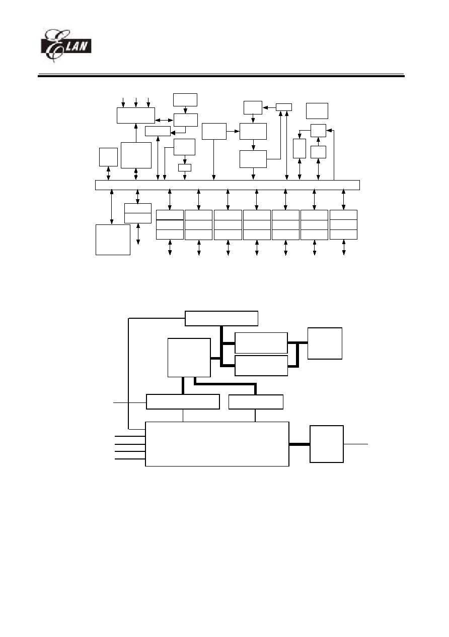
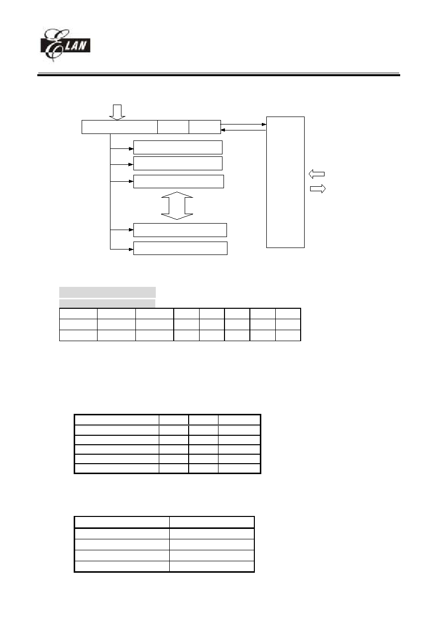
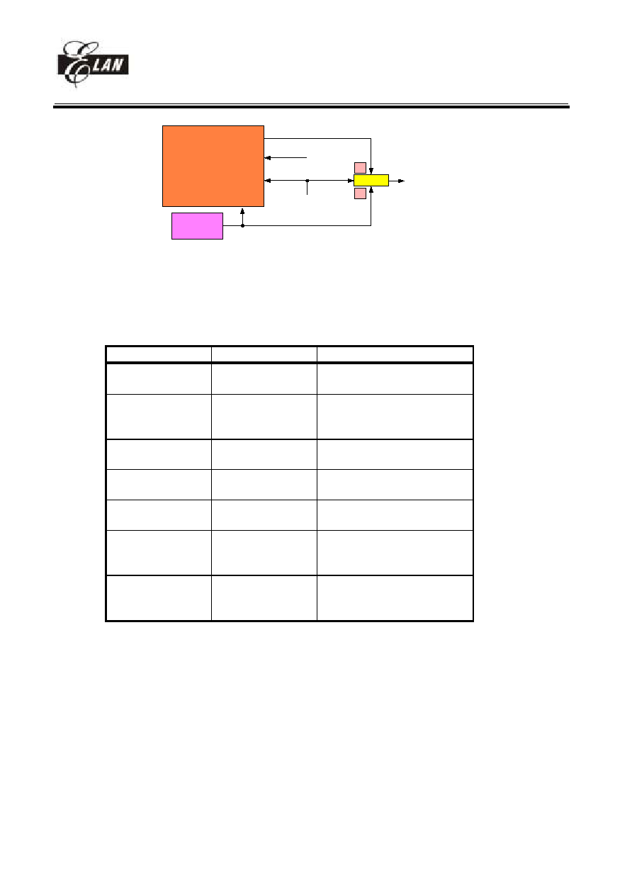
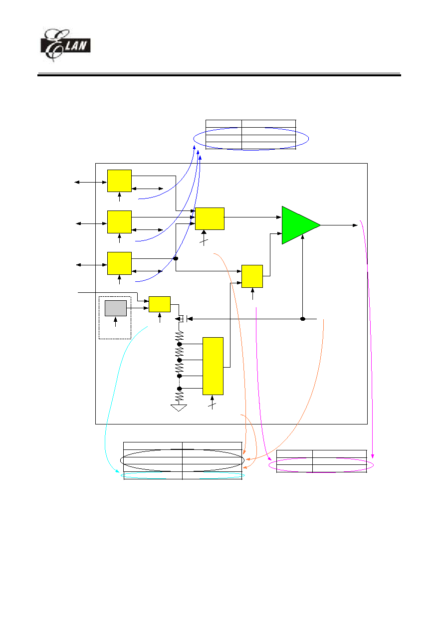
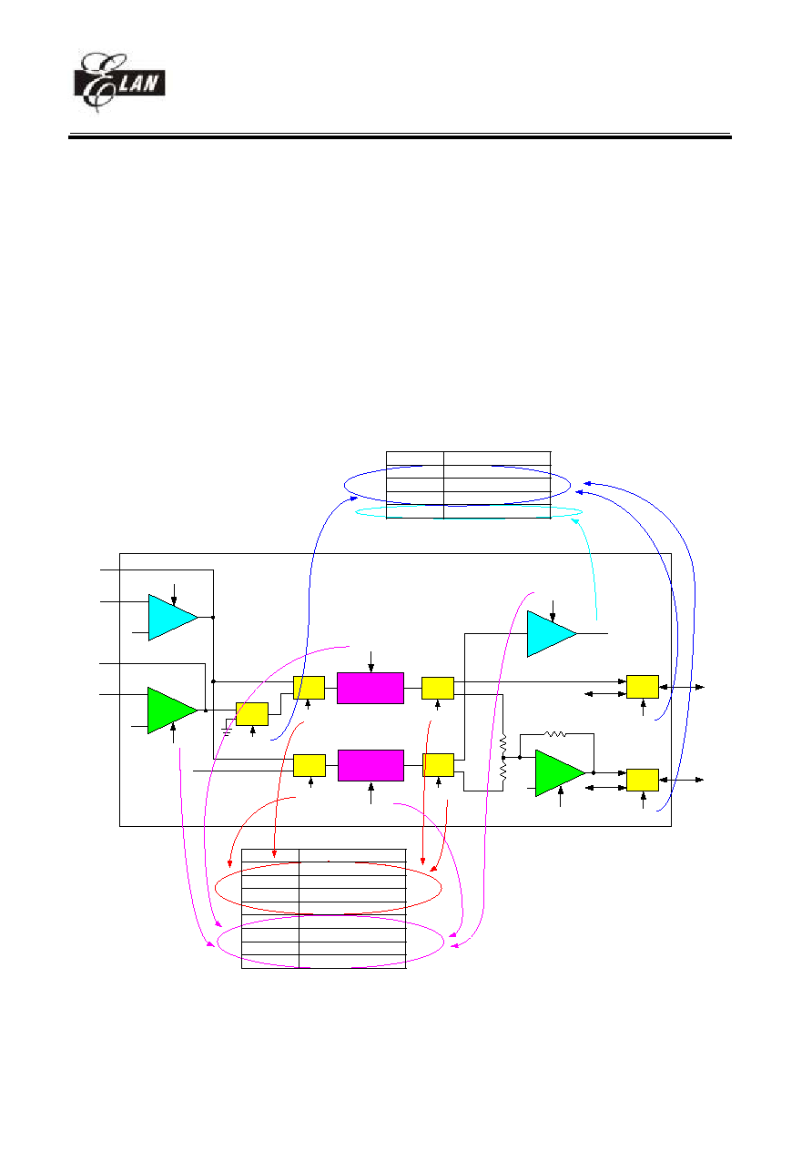
V. Functional Block Diagram
TIMING
CONTROL
TIMER
TCC
COUNTER1
COUNTER2
WDT
OTP ROM
DATA RAM
CONTROL REGISTER
LCD DRIVER
I/O PORT
CPU
8-bit D/A
PROGRAMMING TONE GEN.
CTCSS block
5-bit COMPARATOR
Fig.2a Block diagram
EM78P568
8-bit OTP Micro-controller
__________________________________________________________________________________________________________________________________________________________________
* This specification are subject to be changed without notice.
5
01/31/2004 V4.7
XIN
PLLC
Oscillator
timing control
R1(TCC)
Prescaler
WDT
timer
General
RAM
R4
Interrupt
control
Instruction
decoder
Instruction
register
OTP
ROM
R3
R5
ACC
ALU
STACK
DATA & Control Bus
XOUT
R2
DATA
RAM
Control sleep
and wakeup
on I/O port
P55~P57
D/A
Prog. tone gen.
CTCSS block
Comparator
IOC5
R5
PORT5
P60~P67
IOC6
R6
PORT6
P70~P77
IOC7
R7
PORT7
P80~P87
IOC8
R8
PORT8
P90~P97
IOC9
R9
PORT9
PB0~PB7
IOCB
RB
PORTB
PC0~PC7
IOCC
RC
PORTC
LCD RAM
LCD driver
COM0~COM3
SEG0~SEG31
Fig.2b Block diagram
Fig.2c Block diagram for OTP function
Shift register p to s
OTP aray
Security
register
Configuration
register
Address counter
Power
on reset
High
voltage
detector
OTP control unit
DATA
OEB
PGMB
ACLK
DINCK
VPP
Shift register s to p
EM78P568
8-bit OTP Micro-controller
__________________________________________________________________________________________________________________________________________________________________
* This specification are subject to be changed without notice.
6
01/31/2004 V4.7
VI. Pin Descriptions
PIN I/O DESCRIPTION
POWER
VDD
AVDD
POWER Digital
power
Analog power
VSS
AVSS
POWER Digital
ground
Analog ground
CLOCK
XIN
I
Input pin for 32.768 kHz oscillator
XOUT
O
Output pin for 32.768 kHz oscillator
PLLC
I
Phase loop lock capacitor, connect a capacitor 0.01u to 0.047u to the ground.
LCD
COM0 ~ COM3 O
Common driver pins of LCD drivers
SEG0 ~ SEG9
SEG10 ~ SEG12
SEG13 ~ SEG20
SEG21 ~ SEG28
SEG29 ~ SEG31
O
O (I/O : PORT5)
O (I/O : PORT9)
O (I/O : PORTB)
O (I/O : PORTC)
Segment driver pins of LCD drivers
SEG10 to SEG31 are shared with IO PORT.
Programming
tone generators
TONE
O
Programming single tone or dual tone output
Comparator
CMP1
CMP2
CMP3
I (P62)
I (P63)
I (P64)
Comparator input pins. Shared with PORT62, PORT634 and PORT64.
8-bit D/A
DAO
O (P67)
D/A converter output pin.
Shared with PORT67
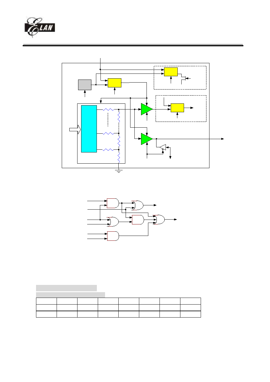
CTCSS
MICO
O
Microphone amplifier output. Put a feedback resistor to adjust the gain
MICI
I
Microphone amplifier input
RXO
O
Receiver amplifier output. Put a feedback resistor to adjust the gain
RXI
I
Receiver amplifier input
AURX
O (P65)
Receiving audio output
Share with PORT65
MTX
O (P66)
Modulation transmission output for CTCSS tone
Shared with PORT66
IO
P55~P57
I/O
PORT5 can be INPUT or OUTPUT port each bit.
PORT5(7:5) are shared with LCD Segment signal.
P60 ~P67
I/O
PORT6 can be INPUT or OUTPUT port each bit.
P70 ~ P77
I/O
PORT7 can be INPUT or OUTPUT port each bit.
PORT7(4~6) are shared with SPI interface pins
Internal Pull high function.
PORT7(0~3) has interrupt function.
EM78P568
8-bit OTP Micro-controller
__________________________________________________________________________________________________________________________________________________________________
* This specification are subject to be changed without notice.
7
01/31/2004 V4.7
P80 ~ P87
I/O
PORT8 can be INPUT or OUTPUT port each bit.
Internal pull high.
PORT85 ~ P87 are shared with ADC input
PORT8(0~3) have wake-up functions(set by RE PAGE0)
P90 ~ P97
I/O
PORT9 can be INPUT or OUTPUT port each bit.
PORT9 are shared with LCD Segment signal.
PB0 ~ PB7
I/O
PORTB can be INPUT or OUTPUT port each bit.
PORTB are shared with LCD Segment signal.
PC0 ~ PC7
I/O
PORTC can be INPUT or OUTPUT port each bit.
PORTC(7:5) are shared with LCD Segment signal.
INT0
(PORT70)
Interrupt sources. Once PORT70 has a falling edge or rising edge signal
(controlled by CONT register), it will generate a interruption.
INT1
(PORT71)
Interrupt sources which has the same interrupt flag. Any pin from PORT71
has a falling edge signal, it will generate a interruption.
INT2
(PORT72)
Interrupt sources which has the same interrupt flag. Any pin from PORT72
has a falling edge signal, it will generate a interruption.
INT3
(PORT73)
Interrupt sources which has the same interrupt flag. Any pin from PORT73
has a falling edge signal, it will generate a interruption.
/RESET I
Low
reset
EM78P568
8-bit OTP Micro-controller
__________________________________________________________________________________________________________________________________________________________________
* This specification are subject to be changed without notice.
8
01/31/2004 V4.7
VII. Functional Descriptions
VII.1 Operational Registers
Register configuration
R PAGE registers
Addr R PAGE0
R PAGE1
R PAGE2
00
Indirect addressing
01
TCC
02
PC
03
Page, Status
04
RAM bank, RSR
05
Port5 I/O data,
Program ROM page
LCD RAM address
06
Port6 I/O data
LCD RAM data buffer
07
Port7 I/O data
CTCSS detection output,
Data RAM bank
08
Port8 I/O data
Data RAM address
09
Port9 I/O data
Data RAM data buffer
0A
PLL, Main clock,
Comparator flag,
WDTE
DAC input data buffer
LCD waveform option
0B
PortB I/O data
0C
PortC I/O data
Counter1 data
0D
LCD control
Counter2 data
0E
Wake-up control,
Interrupt flag
DAC tone selection
0F
Interrupt flag
10
16 bytes
:
Common registers
1F
20
Bank0~Bank3
:
Common registers
3F
(32x8 for each bank)
IOC PAGE registers
Addr IOC PAGE0
IOC PAGE1
00
01
02
03
04
05
Port5 I/O control,
LCD bias control
Comparator control
06
Port6 I/O control
Port6 switches
07
Port7 I/O control
Port7 pull high
08
Port8 I/O control
Port8 pull high
EM78P568
8-bit OTP Micro-controller
__________________________________________________________________________________________________________________________________________________________________
* This specification are subject to be changed without notice.
9
01/31/2004 V4.7
09
Port9 I/O control
Port9 switches
0A
TONE2 control
DAC,DAC tone control,
2.5V ref control
0B
PortB I/O control
0C
PortC I/O control
Port5,8,B,C switch
0D
TONE1 control
Clock source(CN1,CN2)
Prescaler(CN1,CN2)
0E
TONE1 extra control,
Interrupt mask
CTCSS control switches
0F
Interrupt mask
10
:
1F
20
:
3F
VII.2 Operational Register Detail Description
R0 (Indirect Addressing Register)
R0 is not a physically implemented register. It is used as indirect addressing pointer. Any instruction using R0
as register actually accesses data pointed by the RAM Select Register (R4).
Example:
Mov A, @0x20
;store a address at R4 for indirect addressing
Mov 0x04,
A
Mov A, @0xAA
;write data 0xAA to R20 at bank0 through R0
Mov 0x00,
A
R1 (TCC)
TCC data buffer. Increased by 16.384KHz or by the instruction cycle clock (controlled by CONT register).
Written and read by the program as any other register.
R2 (Program Counter)
The structure is depicted in Fig.3.
Generates 16k
× 13 on-chip PROGRAM OTP-ROM addresses to the relative programming instruction codes.
"JMP" instruction allows the direct loading of the low 10 program counter bits.
"CALL" instruction loads the low 10 bits of the PC, PC+1, and then push into the stack.
"RET'' ("RETL k", "RETI") instruction loads the program counter with the contents at the top of stack.
"MOV R2, A" allows the loading of an address from the A register to the PC, and the ninth and tenth bits are
cleared to "0''.
"ADD R2,A" allows a relative address be added to the current PC, and contents of the ninth and tenth bits are
cleared to "0''.
"TBL" allows a relative address added to the current PC, and contents of the ninth and tenth bits don't change.
The most significant bit (A10~A13) will be loaded with the contents of bit PS0~PS3 in the status register (R5
PAGE0) upon the execution of a "JMP'', "CALL'', "ADD R2, A'', or "MOV R2, A'' instruction.
If an interrupt is triggered, PROGRAM ROM will jump to address 0x08 at page0. The CPU will store ACC,
R3 status and R5 PAGE automatically, and they will be restored after instruction RETI.
EM78P568
8-bit OTP Micro-controller
__________________________________________________________________________________________________________________________________________________________________
* This specification are subject to be changed without notice.
10
01/31/2004 V4.7
Fig.3 Program counter organization
R3 (Status, Page selection)
(Status flag, Page selection bits)
7
6
5 4 3 2 1 0
RPAGE2 RPAGE IOCPAGE T
P
Z DC C
R/W-0 R/W-0 R/W-0 R R R/W
R/W
R/W
Bit 0(C) : Carry flag
Bit 1(DC) : Auxiliary carry flag
Bit 2(Z) : Zero flag
Bit 3(P) : Power down bit
Set to 1 during power on or by a "WDTC" command and reset to 0 by a "SLEP" command.
Bit 4(T) : Time-out bit
Set to 1 by the "SLEP" and "WDTC" command, or during power up and reset to 0 by WDT timeout.
EVENT T
P
REMARK
WDT wake up from sleep mode
0
0
WDT time out (not sleep mode)
0
1
/RESET wake up from sleep
1
0
Power up
1
1
Low pulse on /RESET
x
X
x : don't care
Bit 5(IOCPAGE) : change IOC5 ~ IOCE to another page
0/1 IOC page0 / IOC page1
Please refer to VII.1 Operational registers for detail IOC PAGE register configuration.
Bit 6 ~ Bit 7 (RPAGE0 ~ RPAGE1) : change R5 ~ RE to another page
(RPAGE1,RPAGE0)
R page # selected
(0,0)
R page 0
(0,1)
R page 1
(1,0)
R page 2
(1,1)
R page 3
PC
A13 A12 A11 A10 A9 A8 A7~A0
0000
PAGE0 0000~03FF
0001
PAGE1 0400~07FF
1110
PAGE14 3800~3BFF
1111
PAGE15 3C00~3FFF
0010
PAGE2 0800~0BFF
STACK1
STACK2
STACK3
STACK4
STACK5
STACK6
STACK7
STACK8
STACK9
STACK10
STACK11
STACK12
STACK13
STACK14
STACK15
STACK16
CALL and
INTERRUPT
RET
RETL
RETI
ACC,R3,R5(PAGE)
R5(PAGE)
store
restore
EM78P568
8-bit OTP Micro-controller
__________________________________________________________________________________________________________________________________________________________________
* This specification are subject to be changed without notice.
11
01/31/2004 V4.7
Please refer to VII.1 Operational registers for detail R PAGE register configuration.
R4 (RAM selection for common registers R20 ~ R3F))
(RAM selection register)
7 6 5 4 3 2 1 0
RB1 RB0 RSR5 RSR4 RSR3 RSR2 RSR1 RSR0
R/W-0
R/W-0 R/W R/W R/W R/W R/W R/W
Bit 0 ~ Bit 5 (RSR0 ~ RSR5) : Indirect addressing for common registers R20 ~ R3F
RSR bits are used to select up to 32 registers (R20 to R3F) in the indirect addressing mode.
Bit 6 ~ Bit 7 (RB0 ~ RB1) : Bank selection bits for common registers R20 ~ R3F
These selection bits are used to determine which bank is activated among the 4 banks for 32 register (R20 to
R3F)..
Please refer to VII.1 Operational Registers for details.
R5 (PORT5 I/O data, Program page selection, LCD address)
PAGE0 (PORT5 I/O data register, Program page register)
7 6 5 4 3 2 1 0
P57 P56 P55 - PS3 PS2 PS1 PS0
R/W R/W R/W
R/W-0 R/W-0 R/W-0 R/W-0
Bit 0 ~ Bit 3 (PS0 ~ PS3) : Program page selection bits
PS3 PS2 PS1
PS0 Program memory page (Address)
0 0 0 0
Page
0
0 0 0 1
Page
1
0 0 1 0
Page
2
0 0 1 1
Page
3
: : : :
:
: : : :
:
1 1 1 0
Page
14
1 1 1 1
Page
15
User can use PAGE instruction to change page to maintain program page by user. Otherwise, user can use
far jump (FJMP) or far call (FCALL) instructions to program user's code. And the program page is
maintained by EMC's complier. It will change user's program by inserting instructions within program.
Bit 4 : (undefined) not allowed to use
Bit 5 ~ Bit 7 (P55 ~ P57) : 8-bit PORT5(5~7) I/O data register
User can use IOC register to define input or output each bit.
PAGE1 (LCD address)
7 6 5 4 3 2 1 0
- - - -
LCDA3
LCDA2
LCDA1
LCDA0
R/W-0
R/W-0
R/W-0
R/W-0
Bit 0 ~ Bit 3 (LCDA0 ~ LCDA3) : LCD address for LCD RAM read or write
The address of the LCD RAM correspond to the COMMON and SEGMENT signals as the table.
COM3 ~ COM0
LCD address
(LCDA3 ~ LCDA0)
SEG1, SEG0
00H
SEG3, SEG2
01H
SEG5, SEG4
02H
SEG7, SEG6
03H
EM78P568
8-bit OTP Micro-controller
__________________________________________________________________________________________________________________________________________________________________
* This specification are subject to be changed without notice.
12
01/31/2004 V4.7
SEG9, SEG8
04H
SEG11, SEG10
05H
SEG13, SEG12
06H
SEG15, SEG14
07H
SEG17, SEG16
08H
SEG19, SEG18
09H
SEG21, SEG20
0AH
SEG23, SEG22
0BH
SEG25, SEG24
0CH
SEG27, SEG26
0DH
SEG29, SEG28
0EH
SEG31, SEG30
0FH
Bit 4 ~ Bit 7 : (undefined) not allowed to use
R6 (PORT6 I/O data, LCD data)
PAGE0 (PORT6 I/O data register)
7 6 5 4 3 2 1 0
P67 P66 P65 P64 P63 P62 P61 P60
R/W R/W R/W R/W R/W R/W R/W R/W
Bit 0 ~ Bit 8 (P60 ~ P67) : 8-bit PORT6(0~7) I/O data register
User can use IOC register to define input or output each bit.
PAGE1 (LCD data)
7 6 5 4 3 2 1 0
LCDD7 LCDD6 LCDD5 LCDD4
LCDD3
LCDD2
LCDD1
LCDD0
R/W R/W R/W R/W R/W R/W R/W R/W
Bit 0 ~ Bit 7 (LCDD0 ~ LCDD7 ) : LCD data buffer for LCD RAM read or write
LCD data vs. COM-SEG
LCD address
LCDD7 ~ LCDD4 LCDD3 ~ LCDD0
(LCDA3 ~ LCDA0)
COM3 ~ COM0
COM3 ~ COM0
SEG1 SEG0
00H
SEG3 SEG2
01H
SEG5 SEG4
02H
SEG7 SEG6
03H
SEG9 SEG8
04H
SEG11 SEG10
05H
SEG13 SEG12
06H
SEG15 SEG14
07H
SEG17 SEG16
08H
SEG19 SEG18
09H
SEG21 SEG20
0AH
SEG23 SEG22
0BH
SEG25 SEG24
0CH
SEG27 SEG26
0DH
SEG29 SEG28
0EH
SEG31 SEG30
0FH
EM78P568
8-bit OTP Micro-controller
__________________________________________________________________________________________________________________________________________________________________
* This specification are subject to be changed without notice.
13
01/31/2004 V4.7
R7 (PORT7 I/O data, Data RAM bank)
PAGE0 (PORT7 I/O data register)
7 6 5 4 3 2 1 0
P77 P76 P75 P74 P73 P72 P71 P70
R/W R/W R/W R/W R/W R/W R/W R/W
Bit 0 ~ Bit 7 (P70 ~ P77) : 8-bit PORT7(0~7) I/O data register
User can use IOC register to define input or output each bit.
PAGE1 (CTCSS detection output, Data RAM bank selection bits)
7 6 5 4 3 2
1
0
- DETO -
-
-
- RAM_B1
RAM_B0
R R/W-0
R/W-0
Bit 0 ~ Bit1 (RAM_B0 ~ RAM_B1) : Data RAM bank selection bits
Each bank has address 0 ~ address 255 which is total 256 (0.25k) bytes RAM size.
Data RAM bank selection : (Total RAM = 1.0K)
RAM_B1 RAM_B0 RAM
bank
0 0
Bank0
0 1
Bank1
1 0
Bank2
1 1
Bank3
Bit 2 ~ Bit 5 : (undefined) not allowed to use
Bit 6(DETO) : CTCSS tone detection
The signal passing CTCSS sub audio LPF will be extracted CTCSS tone. Then this tone will go into the
ZC(Zero-crossing detector) and output to DETO bit. This bit reflects the CTCSS tone frequency pulse
waveform. The user can count the timing to get the CTCSS frequency. Also see IOCE PAGE1 for CTCSS
block and switch control.
Bit 7 : (undefined) not allowed to use
R8 (PORT8 I/O data, Data RAM address)
PAGE0 (PORT8 I/O data register)
7 6 5 4 3 2 1 0
P87 P86 P85 P84 P83 P82 P81 P80
R/W R/W R/W R/W R/W R/W R/W R/W
Bit 0 ~ Bit 7 (P80 ~ P87) : 8-bit PORT8(0~7) I/O data register
User can use IOC register to define input or output each bit.
PAGE1 (Data RAM address register)
7 6 5 4 3 2 1 0
RAM_A7 RAM_A6 RAM_A5 RAM_A4 RAM_A3 RAM_A2 RAM_A1 RAM_A0
R/W-0 R/W-0 R/W-0 R/W-0 R/W-0 R/W-0 R/W-0 R/W-0
Bit 0 ~ Bit 7 (RAM_A0 ~ RAM_A7) : data RAM address
The data RAM bank's selection is from R7 PAGE1 bit0 ~ bit 1 (RAM_B0 ~ RAM_B1).
R9 (PORT9 I/O data, Data RAM data buffer)
PAGE0 (PORT9 I/O data register)
7 6 5 4 3 2 1 0
P97 P96 P95 P94 P93 P92 P91 P90
R/W R/W R/W R/W R/W R/W R/W R/W
EM78P568
8-bit OTP Micro-controller
__________________________________________________________________________________________________________________________________________________________________
* This specification are subject to be changed without notice.
14
01/31/2004 V4.7
Bit 0 ~ Bit 7 (P90 ~ P97) : 8-bit PORT9(0~7) I/O data register
User can use IOC register to define input or output each bit.
PAGE1 (Data RAM data register)
7 6 5 4 3 2 1 0
RAM_D7 RAM_D6 RAM_D5 RAM_D4 RAM_D3 RAM_D2 RAM_D1 RAM_D0
R/W R/W R/W R/W R/W R/W R/W R/W
Bit 0 ~ Bit 7 (RAM_D0 ~ RAM_D7) : Data RAM's data
The address for data RAM is accessed from R8 PAGE1. The data RAM bank is selected by R7 PAGE1 Bit
0 ~ Bit 1 (RAM_B0 ~ RAM_B1).
RA (PLL, Main clock selection, Comparator flag, Watchdog timer, DAC input data buffer,
LCD option)
PAGE0 (PLL enable bit, Main clock selection bits, Comparator control bits, Watchdog timer enable bit)
7 6 5 4 3 2 1 0
IDLE PLLEN CLK2 CLK1 CLK0 CMPFLAG CMPREF WDTEN
R/W-0 R/W-0 R/W-0 R/W-1 R/W-1
R
R/W-0 R/W-0
Bit 0(WDTEN) : Watch dog control bit
0/1 disable/enable
User can use WDTC instruction to clear watch dog counter. The counter 's clock source is 32768/2 Hz. If
the prescaler assigns to TCC. Watch dog will time out by (1/32768 )*2 * 256 = 15.616mS. If the
prescaler assigns to WDT, the time of time out will be more times depending on the ratio of prescaler.
Bit 1(CMPREF) : Comparator's reference voltage source selection bit
0 Comparator's reference voltage is driven from internal bias resistor string. This reference voltage level
can be set by RD PAGE0 bit 0 ~ bit 5 (CMP_B0 ~ CMP_B5).
1 Comparator's reference voltage is driven from external bias. This reference voltage input is CMP3/P65
pin. Also IOC6 PAGE1 bit 2(CMP63/P63) should be set to "1".
Bit 2(CMPFLAG) : Output of the comparator
0 Input voltage < reference voltage
1 input voltage > reference voltage
Bit 3 ~ Bit 5 (CLK0 ~ CLK2) : MAIN clock selection bits
User can choose different frequency of main clock by CLK1 and CLK2. All the clock selection is list below.
PLLEN
CLK2
CLK1
CLK0
Sub clock
MAIN clock
CPU clock
1 0 0 0
32.768kHz
447.829kHz
447.829kHz
(Normal
mode)
1 0 0 1
32.768kHz
895.658kHz
895.658kHz
(Normal
mode)
1 0 1 0
32.768kHz
1.791MHz
1.791MHz
(Normal
mode)
1 0 1 1
32.768kHz
3.582MHz
3.582MHz
(Normal
mode)
1 1 0 0
32.768kHz
7.165MHz
7.165MHz
(Normal
mode)
1 1 0 1
32.768kHz
10.747MHz
10.747MHz
(Normal
mode)
1 1 1 0
32.768kHz
14.331MHz
14.331MHz
(Normal
mode)
1 1 1 1
32.768kHz
17.913MHz
17.913MHz
(Normal
mode)
0
don't care
don't care 32.768kHz
don't care
32.768kHz (Green mode)
Bit 6(PLLEN) : PLL's power control bit which is CPU mode control register
0/1 disable PLL/enable PLL
If enable PLL, CPU will operate at normal mode (high frequency). Otherwise, it will run at green mode
(low frequency, 32768 Hz).
EM78P568
8-bit OTP Micro-controller
__________________________________________________________________________________________________________________________________________________________________
* This specification are subject to be changed without notice.
15
01/31/2004 V4.7
Sub-clock
32.768kHz
switch
0
1
System clock
PLL circuit
447.8293kHz ~17.9132MHz
ENPLL
CLK2 ~ CLK0
Fig.4 The relation between 32.768kHz and PLL
Bit 7(IDLE) : Sleep mode or IDLE mode control after using "SLEP" instruction.
0/1 SLEEP mode/IDLE mode.
This bit will decide SLEP instruction which mode to go.
The status after wake-up and the wake-up sources list as the table below.
Wakeup signal
SLEEP mode
IDLE mode
RA(7,6)=(0,0)
+ SLEP
RA(7,6)=(1,0)
+ SLEP
TCC time out
IOCF bit0=1
No function
(1) Wake-up
(2) Jump to SLEP next instruction
COUNTER1 time out
IOCF bit1=1
No function
(1) Wake-up
(2) Jump to SLEP next instruction
COUNTER2 time out
IOCF bit2=2
No function
(1) Wake-up
(2) Jump to SLEP next instruction
WDT time out
Reset and jump to
address 0
(1) Wake-up
(2) Next instruction
PORT8(0~3)
RE PAGE0 bit3 or
bit4 or bit5 or bit6 = 1
Reset and Jump to
address 0
(1) Wake-up
(2) Jump to SLEP next instruction
PORT7(0~3)
IOCF bit3 or bit4 or
bit5 or bit7=1
Reset and Jump to
address 0
(1) Wake-up
(2) Jump to SLEP next instruction
<Note> PORT70 's wakeup function is controlled by IOCF bit 3. It's falling edge or rising edge trigger
(controlled by CONT register bit7).
PORT7(1~3) 's wakeup functions are controlled by IOCF bit (4,5,7). They are falling edge trigger.
PORT80~PORT83's wakeup function are controlled by RE PAGE0 bit 0 ~ bit 3. They are falling
edge trigger.
EM78P568
8-bit OTP Micro-controller
__________________________________________________________________________________________________________________________________________________________________
* This specification are subject to be changed without notice.
16
01/31/2004 V4.7
PAGE1 (DAC input data register)
7 6 5 4 3 2 1 0
DA7 DA6 DA5 DA4 DA3 DA2 DA1 DA0
R/W-1 R/W-1 R/W-1 R/W-1 R/W-1 R/W-1 R/W-1 R/W-1
Bit 0 ~ Bit 7 (DA0 to DA7) : DA converter data buffer
PAGE2 (LCD waveform option, Multiplication control)
7 6 5 4 3 2 1 0
LCDOPT
- - - - - - -
R/W-0
Bit 0 ~ Bit 6 : (undefined) not allowed to use
Bit 7 (LCDOPT) : LCD output waveform option
0 default LCD waveform for Type0 LCD waveform
1 switch over LCD bias V1 and V2 for segment for Type1 LCD waveform
(Please set this bit to "1" to get better display performance while LCD driver is used)
RB (PORTB I/O data, ADC output data buffer)
PAGE0 (PORT9 I/O data register)
7 6 5 4 3 2 1 0
PB7 PB6 PB5 PB4 PB3 PB2 PB1 PB0
R/W R/W R/W R/W R/W R/W R/W R/W
Bit 0 ~ Bit 7 (PB0 ~ PB7) : 8-bit PORTB(0~7) I/O data register
User can use IOC register to define input or output each bit.
RC (PORTC I/O data, Counter1 data)
PAGE0 (PORT9 I/O data register)
7 6 5 4 3 2 1 0
PC7 PC6 PC5 PC4 PC3 PC2 PC1 PC0
R/W R/W R/W R/W R/W R/W R/W R/W
Bit 0 ~ Bit 7 (PC0 ~ PC7) : 8-bit PORTC(0~7) I/O data register
User can use IOC register to define input or output each bit.
PAGE1 (Counter1 data register)
Bit7 Bit6 Bit5 Bit4 Bit3 Bit2 Bit1 Bit0
CN17 CN16 CN15 CN14 CN13 CN12 CN11 CN10
R/W-0 R/W-0 R/W-0 R/W-0 R/W-0 R/W-0 R/W-0 R/W-0
Bit 0 ~ Bit 7 (CN10 ~ CN17) : Counter1's buffer that user can read and write.
Counter1 is a 8-bit up-counter with 8-bit prescaler that user can use RC PAGE1 to preset and read the
counter.(write preset) After a interruption , it will reload the preset value.
Example for writing :
MOV 0x0C, A ; write the data at accumulator to counter1 (preset)
Example for reading :
MOV A, 0x0C ; read the data at counter1 to accumulator
RD (LCD control, Counter2 data, PWM1,2 duty latch, Multiplication result)
PAGE0 (LCD driver control bits)
7 6 5 4 3 2 1 0
DETOED
- - - -
LCD_C1 LCD_C0 LCD_M
R/W-0
R/W-0
R/W-0
R/W-0
Bit 0 (LCD_M) : LCD operation method including duty and frame frequency
EM78P568
8-bit OTP Micro-controller
__________________________________________________________________________________________________________________________________________________________________
* This specification are subject to be changed without notice.
17
01/31/2004 V4.7
Bit 1 ~ Bit 2 (LCD_C0 ~ LCD_C1) : LCD display control
LCD_C1 LCD_C0 LCD_M LCD Display Control
Duty Bias
0 0 0
change duty
1/4 1/3
1
Disable(turn off LCD)
1/2 1/3
0 1 :
Blanking
: :
1
1
:
LCD display enable
:
:
Ps. To change the display duty must set the "LCD_C1 ,LCD_C0" to "00".
The controller can drive LCD directly. The LCD block is made up of common driver, segment driver,
display LCD RAM, common output pins, segment output pins and LCD operating power supply. The basic
structure contains a timing control. This timing control uses the basic frequency 32.768KHz to generate the
proper timing for different duty and display access.
RD PAGE0 Bit 0 ~ Bit 2 are LCD control bits for LCD driver. These LCD control bits determine the duty,
the number of common and the frame frequency. The LCD display (disable, enable, blanking) is controlled
by Bit 1 and Bit 2. The driving duty is decided by Bit 0. The display data is stored in LCD RAM which
address and data access controlled by registers R5 PAGE1 and R6 PAGE1.
User can regulate the contrast of LCD display by IOC5 PAGE0 Bit 0 ~ Bit 3 (BIAS0 ~ BIAS3). Up to 16
levels contrast is convenient for better display.
Bit 3 ~ Bit 6 : (undefined) not allowed to use
Bit 7 (DETOED) : the interrupt triggering edge control for CTCSS tone detection output
0/1 falling edge/falling and rising
PAGE1 (Counter2 data register)
Bit7 Bit6 Bit5 Bit4 Bit3 Bit2 Bit1 Bit0
CN27 CN26 CN25 CN24 CN23 CN22 CN21 CN20
R/W-0 R/W-0 R/W-0 R/W-0 R/W-0 R/W-0 R/W-0 R/W-0
Bit 0 ~ Bit 7 (CN20 ~ CN27) : Counter2's buffer that user can read and write.
Counter2 is a 8-bit up-counter with 8-bit prescaler that user can use RD PAGE1 to preset and read the
counter.(write preset) After a interruption, it will reload the preset value.
Example for writing :
MOV 0x0D, A ; write the data at accumulator to counter2 (preset)
Example for reading :
MOV A, 0x0D ; read the data at counter2 to accumulator
RE (Interrupt flag, Wake-up control, DAC tone output frequency selection, PWM2 duty latch,
Multiplication result)
PAGE0 (Interrupt flag, Wake-up control bits)
7 6 5 4 3 2 1 0
- - - -
/WUP83 /WUP82 /WUP81 /WUP80
R/W-0
R/W-0
R/W-0
R/W-0
Bit 0 (/WUP80) : PORT80 wake-up control, 0/1 disable/enable P80 pin wake-up function
Bit 1 (/WUP81) : PORT81 wake-up control, 0/1 disable/enable P81 pin wake-up function
Bit 2 (/WUP82) : PORT82 wake-up control, 0/1 disable/enable P82 pin wake-up function
Bit 3 (/WUP83) : PORT83 wake-up control, 0/1 disable/enable P83 pin wake-up function
Bit 4 ~ Bit 7 :
(undefined) not allowed to use
Set when a selected period is reached, reset by software.
EM78P568
8-bit OTP Micro-controller
__________________________________________________________________________________________________________________________________________________________________
* This specification are subject to be changed without notice.
18
01/31/2004 V4.7
PAGE1 (Programmable D/A tone selection register)
7 6 5 4 3 2 1 0
DAT7 DAT6 DAT5 DAT4 DAT3
DAT2
DAT1
DAT0
R/W-1 R/W-1 R/W-1 R/W-1 R/W-1
R/W-1
R/W-1
R/W-1
Bit 0 ~ Bit 7 (DAT0 ~ DAT7) : D/A tone output frequency selection
The programmable D/A tone output frequency = 447829Hz / Mi / 32, where Mi = DAT7 ~ DAT0 = 1 ~ 255
When Mi = DAT7 ~ DAT0 = 0 or DAT/DAD(IOCA PAGE1 Bit 7) = 0, the D/A tone output generation
circuit will be disabled. It is specially used for CTCSS tone generation. Also refer to DAC for details.
DAC Tone
Gen.
fm =
447.829kHz
MUX
DA7~DA0
DAT/DAD
DAT7~DAT0
to DAC input
Fig.5 Programmable DAC tone generation
For example : CTCSS tone generation table
Channel DAT7~DAT0
D/A tone
generation
CTCSS
tone
Mi
(decimal)
Act.
Freq.
- 00000000
Disable
- - -
1 11010001
Enable
67.0 209
66.960
2 11001010 69.3 202
69.280
3 11000011 71.9 195
71.767
4 10111100 74.4 188
74.440
5 10110110 77.0 182
76.894
6 10110000 79.7 176
79.515
7 10101010 82.5 170
82.322
8 10100100 85.4 164
85.333
9 10011110 88.5 158
88.574
10 10011001 91.5 153 91.468
11 10010100 94.8 148 94.558
12 10010000 97.4 144 97.185
13 10001100 100.0 140 99.962
14 10000111 103.5 135
103.664
15 10000011 107.2 131
106.829
16 01111110 110.9 126
111.069
17
01111010 114.8
122
114.710
18
01110110 118.8
118
118.599
19
01110010 123.0
114
122.760
20
01101110 127.3
110
127.224
21
01101010 131.8
106
132.025
22
01100111 136.5
103
135.870
23
01100011 141.3 99
141.360
24
01100000 146.2 96
145.778
25
01011100 151.4 92
152.116
26
01011001 156.7 89
157.243
27
01011000 159.8 88
159.030
28
01010110 162.2 86
162.729
29
01010011 167.9 83
168.610
EM78P568
8-bit OTP Micro-controller
__________________________________________________________________________________________________________________________________________________________________
* This specification are subject to be changed without notice.
19
01/31/2004 V4.7
30
01010001 173.8 81
172.773
31
01001110 179.9 78
179.419
32 01001100 183.5 76
184.140
33
01001011 186.2 75
186.595
34
01001010 189.9 74
189.117
35
01001001 192.8 73
191.708
36
01000111 196.6 71
197.108
37
01000110 199.5 70
199.924
38
01000101 203.5 69
202.821
39
01000100 206.5 68
205.804
40
01000010 210.7 66
212.040
41
01000000 218.1 64
218.667
42
00111110 225.7 62
225.720
43
00111101 229.1 61
229.421
44
00111100 233.6 60
233.244
45
00111010 241.8 58
241.287
46
00111000 250.3 56
249.905
47
00110111 254.1 55
254.448
RF (Interrupt status)
(Interrupt status register)
7 6 5 4 3 2 1 0
INT3 DETO INT2 INT1 INT0 CNT2 CNT1 TCIF
R/W-0 R/W-0 R/W-0 R/W-0 R/W-0 R/W-0 R/W-0 R/W-0
"1" means interrupt request, "0" means non-interrupt
Bit 0(TCIF) : TCC timer overflow interrupt flag
Set when TCC timer overflows.
Bit 1(CNT1) : counter1 timer overflow interrupt flag
Set when counter1 timer overflows.
Bit 2(CNT2) : counter2 timer overflow interrupt flag
Set when counter2 timer overflows.
Bit 3(INT0) : external INT0 pin interrupt flag
If PORT70 has a falling edge/rising edge (controlled by CONT register) trigger signal, CPU will set this bit.
Bit 4(INT1) : external INT1 pin interrupt flag
If PORT71 has a falling edge trigger signal, CPU will set this bit.
Bit 5(INT2) : external INT2 pin interrupt flag
If PORT72 has a falling edge trigger signal, CPU will set this bit.
Bit 6(DETO) : CTCSS tone detection interrupt flag
If CTCSS detection output signal(R7 PAGE1 bit 6) has an edge signal (falling edge, falling and rising
edge), CPU will set this bit.
Bit 7(INT3) : external INT3 pin interrupt flag
If PORT73 has a falling edge trigger signal, CPU will set this bit.
<Note> IOCF is the interrupt mask register. User can read and clear.
EM78P568
8-bit OTP Micro-controller
__________________________________________________________________________________________________________________________________________________________________
* This specification are subject to be changed without notice.
20
01/31/2004 V4.7
Trigger edge as the table
Signal Trigger
TCC Time
out
COUNTER1 Time
out
COUNTER2 Time
out
INT0 Falling
Rising edge
INT1 Falling
edge
INT2 Falling
edge
DETO Falling
edge
Falling and rising edge
R10~R3F (General Purpose Register)
R10~R3F (Banks 0 ~ 3) : all are general purpose registers.
EM78P568
8-bit OTP Micro-controller
__________________________________________________________________________________________________________________________________________________________________
* This specification are subject to be changed without notice.
21
01/31/2004 V4.7
VII.3 Special Purpose Registers
A (Accumulator)
Internal data transfer, or instruction operand holding
It's not an addressable register.
CONT (Control Register)
7 6 5 4 3 2 1 0
P70EG INT TS RETBK
PAB PSR2 PSR1 PSR0
Bit 0 ~ Bit 2 (PSR0 ~ PSR2) : TCC/WDT prescaler bits
PSR2 PSR1 PSR0 TCC
rate WDT
rate
0 0 0 1:2 1:1
0 0 1 1:4 1:2
0 1 0 1:8 1:4
0 1 1 1:16 1:8
1 0 0 1:32 1:16
1 0 1 1:64 1:32
1 1 0 1:128 1:64
1 1 1 1:256
1:128
Bit 3(PAB) : Prescaler assignment bit
0/1 TCC/WDT
Bit 4(RETBK) : Return value backup control for interrupt routine
0 disable/enable
When this bit is set to 1, the CPU will store ACC,R3 status and R5 PAGE automatically after an interrupt is
triggered. And it will be restored after instruction RETI. When this bit is set to 0, the user need to store ACC,
R3 and R5 PAGE in user program.
Bit 5(TS) : TCC signal source
0 internal instruction cycle clock
1 16.384kHz
Bit 6 (INT) : INT enable flag
0 interrupt masked by DISI or hardware interrupt
1 interrupt enabled by ENI/RETI instructions
Bit 7(P70EG) : interrupt edge type of P70
0 P70 's interruption source is a rising edge signal.
1 P70 's interruption source is a falling edge signal.
CONT register is readable (CONTR) and writable (CONTW).
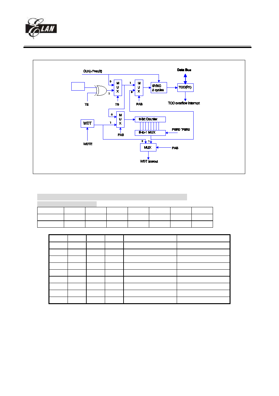
TCC and WDT :
There is an 8-bit counter available as prescaler for the TCC or WDT. The prescaler is available for the TCC
only or WDT only at the same time.
An 8 bit counter is available for TCC or WDT determined by the status of the bit 3 (PAB) of the CONT
register.
See the prescaler ratio in CONT register.
Fig.17 depicts the circuit diagram of TCC/WDT.
Both TCC and prescaler will be cleared by instructions which write to TCC each time.
The prescaler will be cleared by the WDTC and SLEP instructions, when assigned to WDT mode.
The prescaler will not be cleared by SLEP instructions, when assigned to TCC mode.
EM78P568
8-bit OTP Micro-controller
__________________________________________________________________________________________________________________________________________________________________
* This specification are subject to be changed without notice.
22
01/31/2004 V4.7
Fig.6 Block diagram of TCC WDT
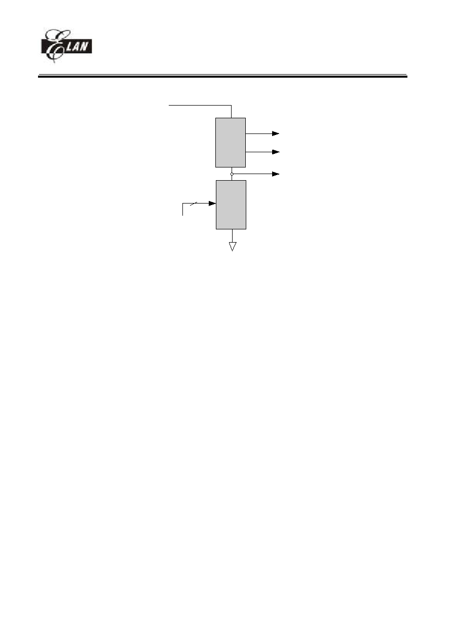
IOC5 (PORT5 I/O control, LCD bias control, Comparator control)
PAGE0 (LCD bias control bits)
7 6 5 4 3 2 1 0
IOC57 IOC56 IOC55
-
BIAS3
BIAS2
BIAS1
BIAS0
R/W-1 R/W-1 R/W-1
R/W-0 R/W-0 R/W-0 R/W-0
Bit 0 ~ Bit 3 (BIAS0 ~ BIAS3) : LCD operation voltage selection. V1 = VDD * (1 - n/60)
BIAS3 BIAS2
BIAS1 BIAS0
Vop (=VDD-VLCD)
Example (VDD = 3V)
0 0 0 0
VDD * (1-0/60)
3V
0 0 0 1
VDD * (1-1/60)
2.95V
0 0 1 0
VDD * (1-2/60)
2.90V
0 0 1 1
VDD * (1-3/60)
2.85V
0 1 0 0
VDD * (1-4/60)
2.80V
: : : :
: :
1 1 0 1
VDD * (1-13/60)
2.35V
1 1 1 0
VDD * (1-14/60)
2.30V
1 1 1 1
VDD * (1-15/60)
2.25V
Bit 4 : (undefined) not allowed to use
Bit 5 ~ Bit 7 (IOC55 ~ IOC57) : PORT5(5~7) I/O direction control register
0 put the relative I/O pin as output
1 put the relative I/O pin into high impedance
16.38KHz
EM78P568
8-bit OTP Micro-controller
__________________________________________________________________________________________________________________________________________________________________
* This specification are subject to be changed without notice.
23
01/31/2004 V4.7
Driver
resistor
and
switch
4
BIAS3 to BIAS0
Bias
resistor
and
switch
VDD
V1
V2
VLCD
Fig.7 LCD driver bias circuit
EM78P568
8-bit OTP Micro-controller
__________________________________________________________________________________________________________________________________________________________________
* This specification are subject to be changed without notice.
24
01/31/2004 V4.7
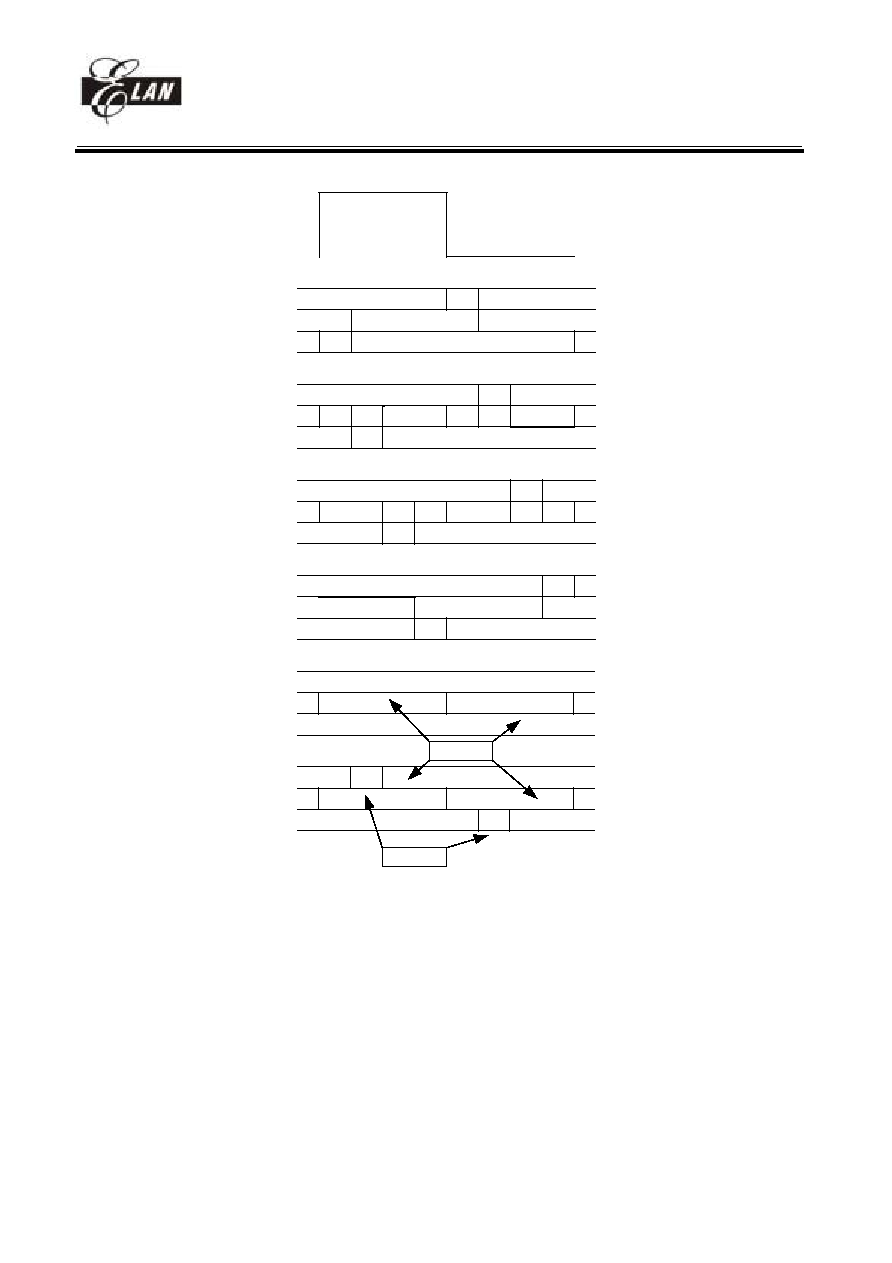
Fig.8a Type0's LCD waveform for 1/3 bias, 1/4 duty
(Type0 or type1 is controlled by RA PAGE2 bit7)
VDD
V1
V2
VLCD
VDD
V1
V2
VLCD
VDD
V1
V2
VLCD
VDD
V1
V2
VLCD
Frame
COM0
COM1
COM2
COM3
VDD
V1
V2
VLCD
VDD
V1
V2
VLCD
SEG
SEG
dark
light
EM78P568
8-bit OTP Micro-controller
__________________________________________________________________________________________________________________________________________________________________
* This specification are subject to be changed without notice.
25
01/31/2004 V4.7
VDD
V1
V2
VLCD
VDD
V1
V2
VLCD
VDD
V1
V2
VLCD
VDD
V1
V2
VLCD
Frame
COM0
COM1
COM2
COM3
VDD
V1
V2
VLCD
VDD
V1
V2
VLCD
SEG
SEG
dark
light
Fig.8b Type1's LCD waveform for 1/3 bias, 1/4 duty
(Type0 or type1 is controlled by RA PAGE2 bit7)
EM78P568
8-bit OTP Micro-controller
__________________________________________________________________________________________________________________________________________________________________
* This specification are subject to be changed without notice.
26
01/31/2004 V4.7
Fig.9a Type0's LCD waveform for 1/3 bias, 1/2 duty
(Type0 or type1 is controlled by RA PAGE2 bit7)
VDD
V1
V2
VLCD
VDD
V1
V2
VLCD
Frame
COM0
COM1
VDD
V1
V2
VLCD
VDD
V1
V2
VLCD
SEG
SEG
dark
light
EM78P568
8-bit OTP Micro-controller
__________________________________________________________________________________________________________________________________________________________________
* This specification are subject to be changed without notice.
27
01/31/2004 V4.7
VDD
V1
V2
VLCD
VDD
V1
V2
VLCD
Frame
COM0
COM1
VDD
V1
V2
VLCD
VDD
V1
V2
VLCD
SEG
SEG
dark
light
Fig.9b Type1's LCD waveform for 1/3 bias, 1/2 duty
(Type0 or type1 is controlled by RA PAGE2 bit7)
PAGE1 (Comparator control register)
7 6 5 4 3 2 1 0
CMPEN CMPS1 CMPS0 CMP_B4 CMP_B3 CMP_B2 CMP_B1 CMP_B0
R/W-0 R/W-0 R/W-0 R/W-0 R/W-0 R/W-0 R/W-0
R/W-0
If user define CMP1/P63 pin, CMP2/P64 pin or CMP3/P65 pin (by CMPIN1, CMPIN2, CMPIN3 at IOCE page1)
as CMP1, CMP2 pin or CMP3 pin (comparator's input pins), user can use this register to control comparator's
function.
Bit 0 ~ Bit 4 (CMP_B0 ~ CMP_B4) : Reference voltage selection of internal bias resistor string
Voltage = VR x ( n + 0.5 )/ 32 , n=0 to 31. Set RB bit 6 (VREF) to select VR = VREG or 2.0V
Bit 5 ~ Bit 6 (CMPS0 ~ CMPS1) : Comparator's channel selection bits from CMP1 to CMP3
Bit 7(CMPEN) : Enable bit of the comparator circuit
0/1 disable/enable the comparator circuit
CMPS1 CMPS0
Input
0 0 CMP1
0 1 CMP2
1 0 CMP3
1 1
Reserved
EM78P568
8-bit OTP Micro-controller
__________________________________________________________________________________________________________________________________________________________________
* This specification are subject to be changed without notice.
28
01/31/2004 V4.7
The relation between these registers is shown as follows in Fig.10.
Ps. VRSEL bit is in IOCA PAGE1 bit 4.
PORT62
MUX
CMP1
P62S
PORT63
MUX
CMP2
P63S
PORT64
MUX
CMP3
P64S
MUX
CMPS1
CMPS0
+
-
MUX
CMPREF
CMPFLAG
CMPEN
0
1
2
CMP1/P62
CMP2/P63
CMP3/P64
MUX
1/2R
R
R
1/2R
5
CMP_B4 to CMP_B0
11111
11110
00000
VRSEL
MUX
2.5V
ref
2.5V
REFEN
(This ckt is form DAC)
VR
VDD
Name
Register bit location
CMPEN
IOC5 PAGE1 bit 7
CMPS1 ~ CMPS0
IOC5 PAGE1 bit 6 ~ 5
CMP_B4 ~ CMP_B0 IOC5 PAGE1 bit 4 ~ 0
Name
Register bit location
CMPREF
RA PAGE0 bit 1
CMPFLAG
RA PAGE0 bit 2
Name
Register bit location
P62S
IOC6 PAGE1 bit 2
P63S
IOC6 PAGE1 bit 3
P64S
IOC6 PAGE1 bit 4
VRSEL
IOCA PAGE1 bit 4
Fig.10 The comparator circuit
EM78P568
8-bit OTP Micro-controller
__________________________________________________________________________________________________________________________________________________________________
* This specification are subject to be changed without notice.
29
01/31/2004 V4.7
Fig.11 The comparator timing
IOC6 (PORT6 I/O control, P6* pins switch control)
PAGE0 (PORT6 I/O control register)
7 6 5 4 3 2 1 0
IOC67 IOC66 IOC65 IOC64
IOC63
IOC62
IOC61
IOC60
R/W-1 R/W-1 R/W-1 R/W-1 R/W-1 R/W-1 R/W-1 R/W-1
Bit 0 ~ Bit 7 (IOC60 ~ IOC67) : PORT6(0~7) I/O direction control register
0 put the relative I/O pin as output
1 put the relative I/O pin into high impedance
PAGE1 (P6* pins switch control register)
7
6 5 4 3 2 1
0
AMUTE
P66S P65S P64S P63S P62S -
-
R/W-0
R/W-0 R/W-0 R/W-0 R/W-0 R/W-0 R/W-0
R/W-0
Bit 0 ~ Bit 1 : (remain these values to "0" unchanged if PORT60,61 are used)
Bit 2(P62S) : Select channel 2 input pin of comparator or I/O PORT63 pin
0 P62 (I/O PORT62) pin is selected
1 CMP1 (Channel 1 input of comparator) pin is selected
Bit 3(P63S) : Select channel 2 input pin of comparator or I/O PORT63 pin
0 P63 (I/O PORT63) pin is selected
1 CMP2 (Channel 2 input of comparator) pin is selected
Bit 4(P64S) : Select channel 3 input pin of comparator or I/O PORT64 pin
0 P64 (I/O PORT64) pin is selected
1 CMP3 (Channel 3 input of comparator) pin is selected
Bit 5(P65S) : Select receiving audio output pin of CTCSS or I/O PORT65 pin
0 P65 (I/O PORT65) pin is selected
1 AURX (Receiving audio output pin of CTCSS) pin is selected
CMPEN
CMP1 to CMP3
reference
voltage
CPU clock
CMPFLAG
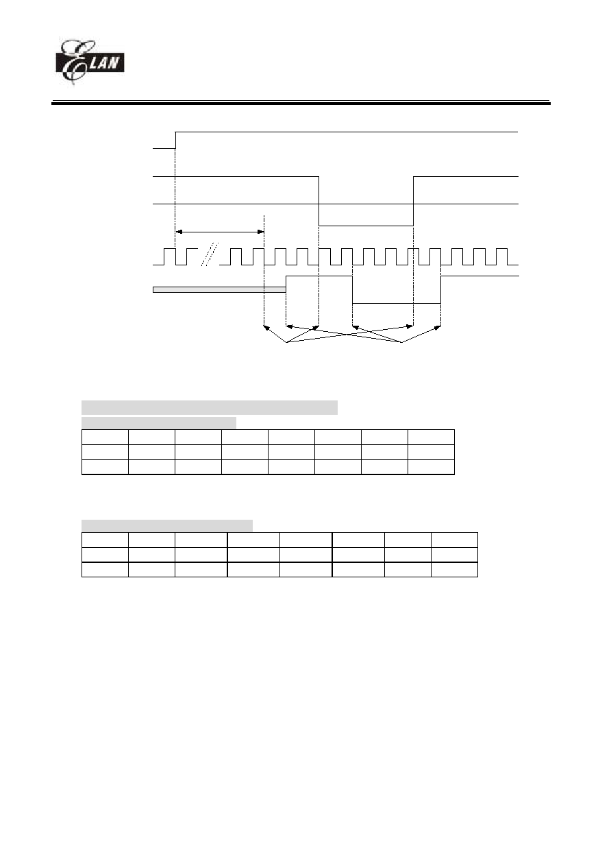
Setup time 10us
Compare start
Compare end
EM78P568
8-bit OTP Micro-controller
__________________________________________________________________________________________________________________________________________________________________
* This specification are subject to be changed without notice.
30
01/31/2004 V4.7
Bit 6(P66S) : Select modulation transmitting output pin of CTCSS or I/O PORT66 pin
0 P66 (I/O PORT66) pin is selected
1 MTX (Modulation transmitting output of CTCSS) pin is selected
Bit 7(AMUTE) : Audio mute for MIC AMP of CTCSS block
0 Voice transmitting path from MIC AMP output
1 Audio mute from MIC AMP output
Refer to Fig.19 CTCSS block for details.
IOC7 (PORT7 I/O control, PORT7 pull high control)
PAGE0 (PORT7 I/O control register)
7 6 5 4 3 2 1 0
IOC77 IOC76 IOC75 IOC74
IOC73
IOC72
IOC71
IOC70
R/W-1 R/W-1 R/W-1 R/W-1 R/W-1 R/W-1 R/W-1 R/W-1
Bit 0 ~ Bit 7 (IOC70 ~ IOC77) : PORT7(0~7) I/O direction control register
0 put the relative I/O pin as output
1 put the relative I/O pin into high impedance
PAGE1 (PORT7 pull high control register)
7 6 5 4 3 2 1 0
PH77 PH76 PH75 PH74 PH73 PH72 PH71 PH70
R/W-0 R/W-0 R/W-0 R/W-0 R/W-0 R/W-0 R/W-0 R/W-0
Bit 0 ~ Bit 7 (PH70 ~ PH77) : PORT7 bit0~bit7 pull high control register
0 disable pull high function.
1 enable pull high function
IOC8 (PORT8 I/O control, PORT8 pull high control)
PAGE0 (PORT8 I/O control register)
7 6 5 4 3 2 1 0
IOC87 IOC86 IOC85 IOC84
IOC83
IOC82
IOC81
IOC80
R/W-1 R/W-1 R/W-1 R/W-1 R/W-1 R/W-1 R/W-1 R/W-1
Bit 0 ~ Bit 7 (IOC80 ~ IOC87) : PORT8(0~7) I/O direction control register
0 put the relative I/O pin as output
1 put the relative I/O pin into high impedance
PAGE1 (PORT8 pull high control register)
7 6 5 4 3 2 1 0
PH87 PH86 PH85 PH84 PH83 PH82 PH81 PH80
R/W-0 R/W-0 R/W-0 R/W-0 R/W-0 R/W-0 R/W-0 R/W-0
Bit 0 ~ Bit 7 (PH80 ~ PH87) : PORT8 bit0~bit7 pull high control register
0 disable pull high function.
1 enable pull high function
IOC9 (PORT9 I/O control, PORT9 switches)
PAGE0 (PORT9 I/O control register)
7 6 5 4 3 2 1 0
IOC97 IOC96 IOC95 IOC94
IOC93
IOC92
IOC91
IOC90
R/W-1 R/W-1 R/W-1 R/W-1 R/W-1 R/W-1 R/W-1 R/W-1
EM78P568
8-bit OTP Micro-controller
__________________________________________________________________________________________________________________________________________________________________
* This specification are subject to be changed without notice.
31
01/31/2004 V4.7
Bit 0 ~ Bit 7 (IOC90 ~ IOC97) : PORT9(0~7) I/O direction control register
0 put the relative I/O pin as output
1 put the relative I/O pin into high impedance
PAGE1 (PORT9 switches)
7 6 5 4 3 2 1 0
P97S P96S P95S P94S P93S P92S P91S P90S
R/W-0 R/W-0 R/W-0 R/W-0 R/W-0 R/W-0 R/W-0 R/W-0
Bit 0(P90S) : Switch I/O PORT90 or LCD segment signal
0 (P90 pin is selected) : normal PORT90
1 (SEG20 pin) : SEGMENT output
Bit 1(P91S) : Switch I/O PORT91 or LCD segment signal
0 (P91 pin is selected) : normal PORT91
1 (SEG19 pin) : SEGMENT output
Bit 2(P92S) : Switch I/O PORT92 or LCD segment signal
0 (P92 pin is selected) : normal PORT92
1 (SEG18 pin) : SEGMENT output
Bit 3(P93S) : Switch I/O PORT93 or LCD segment signal
0 (P93 pin is selected) : normal PORT93
1 (SEG17 pin) : SEGMENT output
Bit 4(P94S) : Switch I/O PORT94 or LCD segment signal
0 (P94 pin is selected) : normal PORT94
1 (SEG16 pin) : SEGMENT output
Bit 5(P95S) : Switch I/O PORT95 or LCD segment signal
0 (P95 pin is selected) : normal PORT95
1 (SEG15 pin) : SEGMENT output
Bit 6(P96S) : Switch I/O PORT96 or LCD segment signal
0 (P96 pin is selected) : normal PORT96
1 (SEG14 pin) : SEGMENT output
Bit 7(P97S) : Switch I/O PORT97 or LCD segment signal
0 (P97 pin is selected) : normal PORT97
1 (SEG13 pin) : SEGMENT output
IOCA (TONE2 control, Control bits for DAC, DAC tone, Reference)
PAGE0 (TONE2 control register)
7 6 5 4 3 2 1 0
T27 T26 T25 T24 T23 T22 T21 T20
R/W-0 R/W-0 R/W-0 R/W-0 R/W-0 R/W-0 R/W-0 R/W-0
Bit 0 ~ Bit 7(T20 ~ T27) : Tone generator 2 `s frequency divider and power control
Please Run in Normal mode .
Clock source = 111957Hz
T27~T20 = `11111111' => Tone generator2 will has 438Hz SIN wave output.
:
T27~T20 = `00000010' => Tone generator2 will has 55921Hz SIN wave output.
T27~T20 = `00000001' => DC bias voltage output
T27~T20 = `00000000' => Power off
Built-in tone generators can generate dialing tone signals for telephone of dialing tone type or just a single
tone. In DTMF application, there are two kinds of tone. One is the group of row frequency (TONE1), the
EM78P568
8-bit OTP Micro-controller
__________________________________________________________________________________________________________________________________________________________________
* This specification are subject to be changed without notice.
32
01/31/2004 V4.7
other is the group of column frequency (TONE2), each group has 4 kinds of frequency, user can get 16
kinds of DTMF frequency totally. Tone generator contains a row frequency sine wave generator for
generating the DTMF signal which selected by IOCD PAGE0, IOCE PAGE0 and a column frequency sine
wave generator for generating the DTMF signal which selected by IOCA PAGE0. This block can generate
single tone by filling one of these two register.
If all the values are low, the power of tone generators will turn off .
TONE2 (IOCA PAGE0) High group freq.
1203.8
(0X5D)
1332.8(0X54)
1473.1(0X4C)
1646.4(0X44)
TONE1(IOCD,
699.7Hz(0x0A0)
1 2 3 A
IOCE
PAGE0)
772.1Hz(0x091)
4 5 6 B
Low group freq. 854.6Hz(0x083)
7
8
9
C
940.8Hz(0x077) *
0
#
D
PAGE1 (Control bits for DAC, DAC tone, Reference)
7 6 5 4 3 2 1 0
DAT/DAD VREF DATEN VRSEL DAST/P67
-
-
-
R/W-0 R/W-0 R/W-0 R/W-0 R/W-0
Bit 0 ~ Bit 2 : (undefined) not allowed to use
Bit 3(DAST/P67) : DAC enable control or P67 switch
0 switch DAO/P67 pin as normal I/O P67
1 enable DAC, enable DAC output buffer B1 and DAC output to DAO/P67 pin
When this bit is set by software, the DA converter will start converting and output to DAO/P67 pin. If user
clean this bit, DA converter will stop and DAO/P67 pin will be become normal I/O P67.
Also refer to bit 5(DATEN) for DAC power control.
Bit 4(VRSEL) : Reference voltage selection bit for Comparator circuit
0/1 VDD/2.5V from DAC
Also see Fig.16 in the next page.
Bit 5(DATEN) : DAC enable control
0/1 disable/enable DAC and its tone output buffer B2
When this bit is set by software, the DA converter will start converting and output to internal CTCSS
VTX3 end. If user clean this bit, DA converter will stop and DAO tone output buffer B2 is disabled.
Also refer to bit 3(DAST/P67) for DAC power control.
Bit 6(VREF) : Reference voltage selection bit for DA converter circuit
DAC reference setting is shown as following. Also see Fig.16 and Fig.17 in the next page.
ASW3 VREF DATEN DAST/P67 Function
1
x
1
x
select 2.5V ref, enable 2.5V ref, enable DAC,
0
1
1
x
enable buffer B2, buffer B2 output to CTCSS LPF
0
0
1
x
select VDD, disable 2.5V, enable DAC, enable buffer B2
x
1
0
1
select 2.5V ref, enable 2.5V ref, enable DAC, enable buffer B1,
buffer B1 output to DAO/P67 pin
x
0
0
1
select VDD, disable 2.5V, enable DAC, enable buffer B1, buffer B1
output to DAO/P67 pin
Ps. IOCE PAGE1 bit 2 (ASW3), IOCA PAGE1 bit 6 (VREF), IOCA PAGE1 bit 5 (DATEN),IOCA PAGE1
bit 3 (DAST/P67)
EM78P568
8-bit OTP Micro-controller
__________________________________________________________________________________________________________________________________________________________________
* This specification are subject to be changed without notice.
33
01/31/2004 V4.7
DAST/P67
PORT67
DAO/P67
DATEN
MUX
2.5V
ref
VDD
REFSEL
REFEN
B2
B1
2R
2R
R
2R
2R
R
8-bit
DAC
input
data
buffer
(This circuit is from Comparator)
VRSEL
To ladder resistors
CMPEN
(This circuit is from CTCSS)
MUX
ASW3
VTX3
VRX3
To Sub-Audio LPF
MUX
DAC input
Fig.12 D/A converter (DAC)
Fig.13 DAC reference voltage control logic
Bit 7 (DAT/DAD) : Programmable D/A tone generation or D/A input data enable control
0 Enable D/A input data and disable D/A tone generation (also stop to D/A tone generation)
1 Enable Programmable D/A tone generation and disable D/A input data
IOCB (PORTB I/O control)
PAGE0 (PORTB I/O control register)
7 6 5 4 3 2 1 0
IOCB7 IOCB6 IOCB5 IOCB4
IOCB3
IOCB2
IOCB1
IOCB0
R/W-1 R/W-1 R/W-1 R/W-1 R/W-1 R/W-1 R/W-1 R/W-1
Bit 0 ~ Bit 7 (IOCB0 ~ IOCB7) : PORTB(0~7) I/O direction control register
0 put the relative I/O pin as output
1 put the relative I/O pin into high impedance
ASW3
DATEN
VREF
DAST/P67
REFSEL
REFEN
CMPEN
VRSEL
EM78P568
8-bit OTP Micro-controller
__________________________________________________________________________________________________________________________________________________________________
* This specification are subject to be changed without notice.
34
01/31/2004 V4.7
IOCC (PORTC I/O control, ADC control)
PAGE0 (PORTC I/O control register)
7 6 5 4 3 2 1 0
IOCC7 IOCC6 IOCC5 IOCC4
IOCC3
IOCC2
IOCC1
IOCC0
R/W-1 R/W-1 R/W-1 R/W-1 R/W-1 R/W-1 R/W-1 R/W-1
Bit 0 ~ Bit 7 (IOCC0 ~ IOCC7) : PORTC(0~7) I/O direction control register
0 put the relative I/O pin as output
1 put the relative I/O pin into high impedance
PAGE1 (PORT switch)
7 6 5 4 3 2 1 0
PC7S PC6S PC5S PBSH PBSL P5SH -
-
R/W-0 R/W-0 R/W-0 R/W-0 R/W-0 R/W-0
R/W-0
Bit 0 : (remain its value to "0" unchanged otherwise Comparator and CTCSS function will fail)
Bit 1: (undefined) not allowed to use
Bit 2(P5SH) : Switch I/O PORT5 high nibble(5~7) or LCD segment signal
0 (P55 ~ P57 pins are selected) : normal PORT5 high nibble(5~7)
1 (SEG10 ~ SEG12 pins are selected) : SEGMENT output
Bit 3(PBSL) : Switch I/O PORTB low nibble(0~3) or LCD segment signal
0 (PB0 ~ PB3 pins are selected) : normal PORTB low nibble(0~3)
1 (SEG28 ~ SEG25 pins are selected) : SEGMENT output
Bit 4(PBSH) : Switch I/O PORTB high nibble(4~7) or LCD segment signal
0 (PB5 ~ PB7 pins are selected) : normal PORTB high nibble(4~7)
1 (SEG24 ~ SEG21 pins are selected) : SEGMENT output
Bit 5(PC5S) : Switch I/O PORTC5 or LCD segment signal
0 (PC5 pin is selected) : normal PORTC5
1 (SEG31 pin) : SEGMENT output
Bit 6(PC6S) : Switch I/O PORTC6 or LCD segment signal
0 (PC6 pin is selected) : normal PORTC6
1 (SEG30 pin) : SEGMENT output
Bit 7(PC7S) : Switch I/O PORTC7 or LCD segment signal
0 (PC7 pin is selected) : normal PORTC7
1 (SEG29 pin) : SEGMENT output
IOCD (TONE1 control, Clock source, Prescaler of CN1 and CN2)
PAGE0 (TONE1 control)
7 6 5 4 3 2 1 0
T17 T16 T15 T14 T13 T12 T11 T10
R/W-0 R/W-0 R/W-0 R/W-0 R/W-0 R/W-0 R/W-0 R/W-0
Bit 0 ~ Bit 7 (T10 ~ T17) : Tone generator 1`s frequency divider and power control
Please Run in Normal mode.
Clock source = 111957Hz and Freq. = 111957Hz / N, where N is divider value for T1A ~ T10 (T1A ~ T18
are in the IOCE PAGE0 Bit 2 ~ Bit 0.
If T20 ~ T18 are all "0", then
T17 ~ T10 = `11111111' => Tone generator1 will has 439Hz SIN wave output.
:
T17~T10 = `00000010' => Tone generator1 will has 55978Hz SIN wave output.
T17~T10 = `00000001' => DC bias voltage output
T17~T10 = `00000000' => Power off
EM78P568
8-bit OTP Micro-controller
__________________________________________________________________________________________________________________________________________________________________
* This specification are subject to be changed without notice.
35
01/31/2004 V4.7
PAGE1 (Clock source and prescaler for COUNTER1 and COUNTER2)
7 6 5 4 3 2 1 0
CNT2S C2_PSC2 C2_PSC1 C2_PSC0
CNT1S C1_PSC2
C1_PSC1 C1_PSC0
R/W-0 R/W-0 R/W-0 R/W-0 R/W-0 R/W-0 R/W-0 R/W-0
Bit 0 ~ Bit 2 (C1_PSC0 ~ C1_PSC2) : COUNTER1 prescaler ratio
C1_PSC2 C1_PSC1 C1_PSC0 COUNTER1
0 0 0 1:2
0 0 1 1:4
0 1 0 1:8
0 1 1 1:16
1 0 0 1:32
1 0 1 1:64
1 1 0 1:128
1 1 1 1:256
Bit 3(CNT1S) : COUNTER1 clock source
0/1 16.384kHz/system clock
Bit 4 ~ Bit 6 (C2_PSC0 ~ C2_PSC2) : COUNTER2 prescaler ratio
C2_PSC2 C2_PSC1 C2_PSC0 COUNTER2
0 0 0 1:2
0 0 1 1:4
0 1 0 1:8
0 1 1 1:16
1 0 0 1:32
1 0 1 1:64
1 1 0 1:128
1 1 1 1:256
Bit 7(CNT2S) : COUNTER2 clock source
0/1 16.384kHz/system clock
IOCE (Interrupt mask, TONE1 extra control bits, CTCSS control switches)
PAGE0 (Interrupt mask, TONE1 extra three control bits)
7 6 5 4 3 2 1 0
- - - - -
T1A
T19
T18
R/W-0 R/W-0 R/W-0 R/W-0
R/W-0 R/W-0 R/W-0
Bit 0 ~ Bit 2 (T18 ~ T1A) : Most significant 3 bits of Tone generator 1`s frequency divider and power control
These 3 bits and other 8 bits (IOCA PAGE0 bit 7 ~ bit0) are assembled as 11-bit frequency divider for Tone
generator 1
Bit 3 : (undefined) not allowed to use
Bit 4 ~ Bit 7 : (remain these values to "0"othwise it will generate unpredicted interrupts)
PAGE1 (CTCSS control switches)
7 6 5 4 3 2 1 0
TXPWR RXPWR BPFPWR LPFPWR
ASW4
ASW3
ASW2
ASW1
R/W-0 R/W-0 R/W-0 R/W-0 R/W-0 R/W-0 R/W-0 R/W-0
Bit 0(ASW1) : Analog switch-1 control for multi-plexer in the CTCSS block
0 Select VRX1 input
1 Select VTX1 input
EM78P568
8-bit OTP Micro-controller
__________________________________________________________________________________________________________________________________________________________________
* This specification are subject to be changed without notice.
36
01/31/2004 V4.7
Bit 1(ASW2) : Analog switch-2 control for multi-plexer in the CTCSS block
0 Select VRX2 output
1 Select VTX2 output
Bit 2(ASW3) : Analog switch-3 control for multi-plexer in the CTCSS block
0 Select VRX3 input
1 Select VTX3 input
Bit 3(ASW4) : Analog switch-4 control for multi-plexer in the CTCSS block
0 Select VRX4 output
1 Select VTX4 output
Bit 4(LPFPWR) : Power control for sub-audio LPF in the CTCSS block. 0/1 disable/enable
Bit 5(BPFPWR) : Power control for audio BPF in the CTCSS block. 0/1 disable/enable
Bit 6(RXPWR) : RX power control for the CTCSS block 0/1 disable/enable
Bit 7(TXPWR) : TX power control for the CTCSS block 0/1 disable/enable
Audio
BPF
VRF
VRF
Rx AMP
MIC AMP
Z C
AURX/P65
RXO
RXI
MICI
MICO
Summing
MTX/P66
VRF
-10dB
0dB
ASW1
ASW2
RXPWR
LPFPWR
BPFPWR
Sub-Audio
LPF
ASW4
MUX
PORT66
MTX
MUX
PORT65
AURX
P65S
P66S
AMP
MUX
ASW3
MUX
MUX
MUX
DETO
TXPWR
TXPWR
RXPWR
VRX1
VTX1
VRX2
VTX2
VRX3
VTX3
VRX4
VTX4
(from DAC output buffer B2)
CTCSS tone input
MUX
MICO
AMUTE
Name
Register bit location
ASW1
IOCE PAGE1 bit 0
ASW2
IOCE PAGE1 bit 1
ASW3
IOCE PAGE1 bit 2
ASW4
IOCE PAGE1 bit 3
LPFPWR
IOCE PAGE1 bit 4
BPFPWR
IOCE PAGE1 bit 5
RXPWR
IOCE PAGE1 bit 6
TXPWR
IOCE PAGE1 bit 7
Name
Register bit location
P65S
IOC6 PAGE1 bit 5
P66S
IOC6 PAGE1 bit 6
AMUTE
IOC6 PAGE1 bit 7
DETO
R7 PAGE1 bit 6
Fig.14 CTCSS block
EM78P568
8-bit OTP Micro-controller
__________________________________________________________________________________________________________________________________________________________________
* This specification are subject to be changed without notice.
37
01/31/2004 V4.7
IOCF (Interrupt mask)
(Interrupt mask register)
Bit7 Bit6 Bit5 Bit4 Bit3 Bit2 Bit1 Bit0
INT3 DETO INT2 INT1 INT0 CNT2 CNT1 TCIF
R/W-0 R/W-0 R/W-0 R/W-0 R/W-0 R/W-0 R/W-0 R/W-0
Bit 0 ~ 7 : interrupt enable bit
0 disable interrupt
1 enable interrupt
The status after interrupt and the interrupt sources list as the table below.
Interrupt signal
IDLE mode
GREEN mode
NORMAL mode
RA(7,6)=(1,0)
+ SLEP
RA(7,6)=(x,0)
no SLEP
RA(7,6)=(x,1)
no SLEP
TCC time out
IOCF bit0=1
And "ENI"
(1) Wake-up
(2) Interrupt (jump to address 8 at
page0)
(3) after RETI instruction, jump to
SLEP Next instruction
Interrupt
(jump to address 8 at
page0)
Interrupt
(jump to address 8 at
page0)
COUNTER1 time out
IOCF bit1=1
And "ENI"
(1) Wake-up
(2)Interrupt (jump to address 8 at
page0)
(3) after RETI instruction, jump to
SLEP Next instruction
Interrupt
(jump to address 8 at
page0)
Interrupt
(jump to address 8 at
page0)
COUNTER2 time out
IOCF bit2=2
And "ENI"
(1) Wake-up
(2) Interrupt (jump to address 8 at
page0)
(3) after RETI instruction, jump to
SLEP Next instruction
Interrupt
(jump to address 8 at
page0)
Interrupt
(jump to address 8 at
page0)
PORT7(0~3)
IOCF bit3 or bit4 or
bit5 or bit7=1
And "ENI"
(1) Wake-up
(2) Interrupt (jump to address 8 at
page0)
(3) after RETI instruction, jump to
SLEP Next instruction
Interrupt
(jump to address 8 at
page0)
Interrupt
(jump to address 8 at
page0)
DETO
IOCF bit6 = 1
And "ENI"
No function
No function
Interrupt
(jump to address 8 at
page0)
<Note> PORT70 's interrupt function is controlled by IOCF bit 3. It's falling edge or rising edge trigger
(controlled by CONT register bit7).
PORT7(1~3) 's wakeup functions are controlled by IOCF bit (4,5,7). They are falling edge trigger.
DETO's interrupt function is controlled by IOCF bit 6. It's falling edge trigger, falling and rising
edge trigger (set by RD PAGE0 bit 7).
<ps> It only happens when master and 16.386kHz mode is selected.
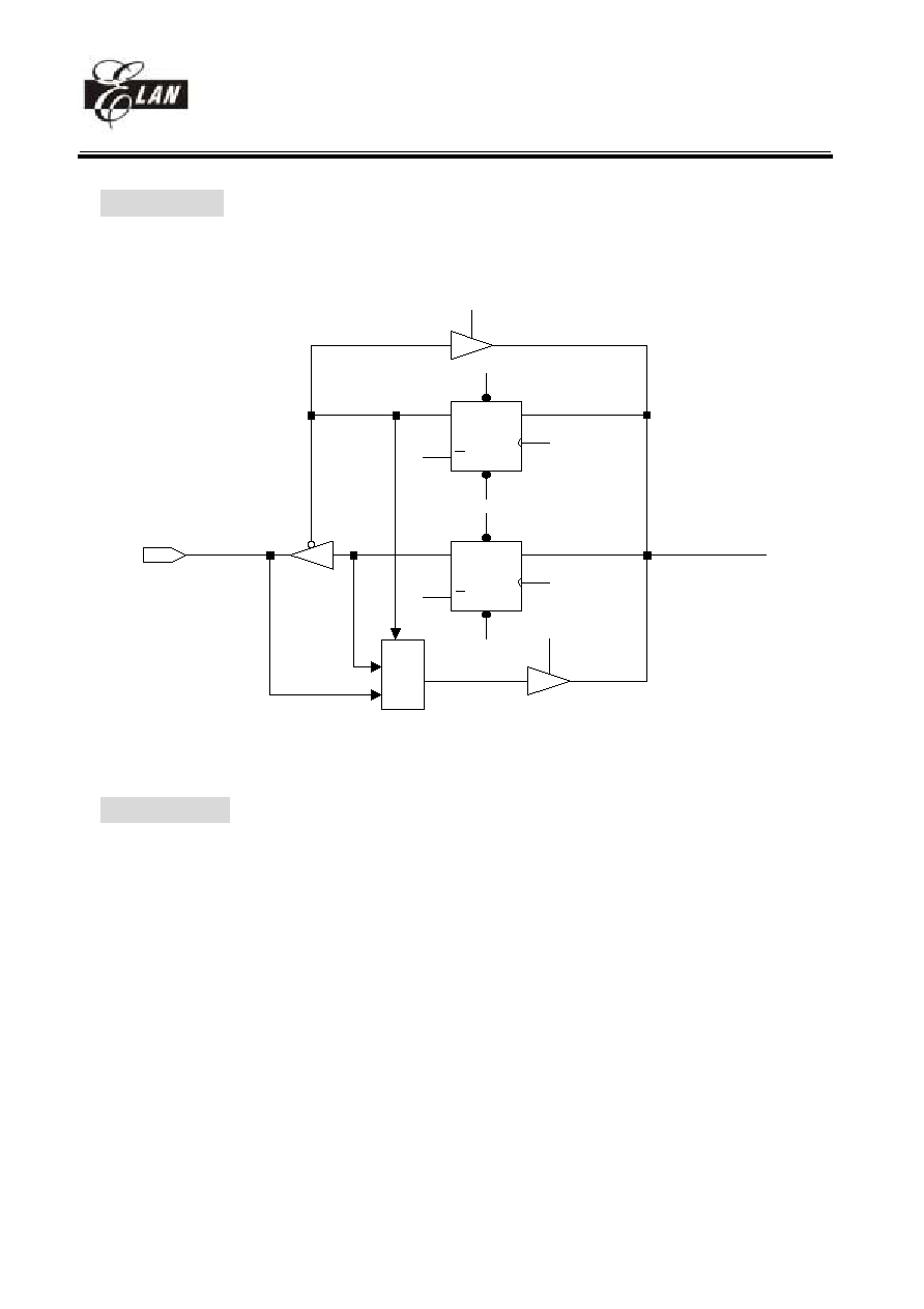
EM78P568
8-bit OTP Micro-controller
__________________________________________________________________________________________________________________________________________________________________
* This specification are subject to be changed without notice.
38
01/31/2004 V4.7
VII.4 I/O Port
The I/O registers are bi-directional tri-state I/O ports. The I/O ports can be defined as "input" or "output" pins by
the I/O control registers under program control. The I/O data registers and I/O control registers are both readable
and writable. The I/O interface circuit is shown as follows.
Fig.15 The circuit of I/O port and I/O control register
VII.5 RESET
The RESET can be caused by
(1) Power on voltage detector reset (/POVD) and power on reset
(2) WDT timeout. (if enabled and in GREEN or NORMAL mode)
(3) /RESET pin pull low
<Note> At case (1), /POVD is controlled by CODE OPTION. If you enable /POVD, CPU will reset at under
1.8V and CPU will consume more current about 5uA. It is used for low voltage reset/ And the power-on
reset is a circuit which is always enabled and only works on initially power-on reset. It will reset CPU at
about 1.4V and consume about 0.5uA.
Once the RESET occurs, the following functions are performed.
· The oscillator is running, or will be started.
· The Program Counter (R2) is set to all "0".
· When power on, the upper 3 bits of R3 and the upper 2 bits of R4 are cleared.
· The Watchdog timer and prescaler counter are cleared.
· The Watchdog timer is disabled.
· The CONT register is set to all "1"
· The other register (bit 7 ~ bit 0) defult values are as follows.
M
U
X
0
1
PDRD
PDWR
CLK
C
L
P
R
D
Q
Q
CLK
C
L
P
R
D
Q
Q
PCWR
IOD
PCRD
PORT
EM78P568
8-bit OTP Micro-controller
__________________________________________________________________________________________________________________________________________________________________
* This specification are subject to be changed without notice.
39
01/31/2004 V4.7
Operation registers :
Address R
register
PAGE0
R register
PAGE1
R register
PAGE2
IOC register
PAGE0
IOC register
PAGE1
0x4
00xxxxxx
0x5 xxxx0000
xxxx0000 111x0000
00000000
0x6 xxxxxxxx xxxxxxxx
11111111 00000000
0x7 xxxxxxxx xxxxxx00
11111111 00000000
0x8 xxxxxxxx 00000000 11111111
00000000
0x9 xxxxxxxx xxxxxxxx
11111111 00000000
0xA 00011x00 11111111 0xxxxxxx
00000000 00000xxx
0xB xxxxxxxx
11111111
0xC xxxxxxxx 00000000 11111111
000000x0
0xD 0xxxx000
00000000 00000000
00000000
0xE xxxx0000
11111111 0000x000
00000000
0xF
00000000
00000000
VII.6 Wake-up
The controller has two types of sleep mode for power saving :
(1) SLEEP mode, RA(7) = 0 + "SLEP" instruction
The controller will turn off all the CPU and crystal. Other circuit with power control like key tone control or
PLL control (which has enable register), user has to turn it off by software.
(2) IDLE mode, RA(7) = 1 + "SLEP" instruction.
The controller will turn CPU off, but the crystal.
Wake-up from SLEEP mode
(1) WDT time out
(2) External interrupt
(3) /RESET pull low
All these cases will reset controller , and run the program at address zero. The status just like the power on reset.
Be sure to enable circuit at case (1) or (2).
Wake-up from IDLE mode
(1)WDT time out
(2) external interrupt
(3) internal interrupt like counters
All these cases, user has to enable circuit before entering IDLE mode. After wake-up, all the register will keep
values just like into "SLEP" instruction before.
At case (2) or (3), controller will wake up and jump to address 0x08 for interruption sub-routine. After finishing
sub-routine ("RETI" instruction), program will jump to the next instruction from "SLEP" instruction.
VII.7 Interrupt
RF is the interrupt status register which records the interrupt request in flag bit. IOCF is the interrupt mask
register. Global interrupt is enabled by ENI instruction and is disabled by DISI instruction. When one of the
interrupts (when enabled) generated, will cause the next instruction to be fetched from address 008H. Once in the
interrupt service routine, the source of the interrupt can be determined by polling the flag bits in the RF register.
EM78P568
8-bit OTP Micro-controller
__________________________________________________________________________________________________________________________________________________________________
* This specification are subject to be changed without notice.
40
01/31/2004 V4.7
The interrupt flag bit must be cleared in software before leaving the interrupt service routine and enabling
interrupts to avoid recursive interrupts.
VII.8 Instruction Set
Instruction set has the following features:
(1) Every bit of any register can be set, cleared, or tested directly.
(2) The I/O register can be regarded as general register. That is, the same instruction can operates on I/O
register.
The symbol "R" represents a register designator which specifies which one of the 64 registers (including
operational registers and general purpose registers) is to be utilized by the instruction. Bits 6 and 7 in R4
determine the selected register bank. "b'' represents a bit field designator which selects the number of the bit,
located in the register "R'', affected by the operation. "k'' represents an 8 or 10-bit constant or literal value.
INSTRUCTION BINARY
HEX
MNEMONIC
OPERATION
STATUS
AFFECTED
Instruction
cycle
0 0000 0000 0000
0000
NOP
No Operation
None
1
0 0000 0000 0001
0001
DAA
Decimal Adjust A
C
1
0 0000 0000 0010
0002
CONTW
A
CONT
None
1
0 0000 0000 0011
0003
SLEP
0
WDT, Stop oscillator
T,P
1
0 0000 0000 0100
0004
WDTC
0
WDT
T,P
1
0 0000 0000 rrrr
000r
IOW R
A
IOCR
None
1
0 0000 0001 0000
0010
ENI
Enable Interrupt
None
1
0 0000 0001 0001
0011
DISI
Disable Interrupt
None
1
0 0000 0001 0010
0012
RET
[Top of Stack]
PC
None
2
0 0000 0001 0011
0013
RETI
[Top of Stack]
PC
Enable Interrupt
None 2
0 0000 0001 0100
0014
CONTR
CONT
A
None
1
0 0000 0001 rrrr
001r
IOR R
IOCR
A
None
1
0 0000 0010 0000
0020
TBL
R2+A
R2 bits 9,10 do not
clear
Z,C,DC 2
0 0000 0011 0000
0030
MUL
(MR) (+/-) (s/us X)*(s/us Y)
MR
None 1
0 0000 01rr rrrr
00rr
MOV R,A
A
R
None
1
0 0000 1000 0000
0080
CLRA
0
A
Z
1
0 0000 11rr rrrr
00rr
CLR R
0
R
Z
1
0 0001 00rr rrrr
01rr
SUB A,R
R-A
A
Z,C,DC
1
0 0001 01rr rrrr
01rr
SUB R,A
R-A
R
Z,C,DC
1
0 0001 10rr rrrr
01rr
DECA R
R-1
A
Z
1
0 0001 11rr rrrr
01rr
DEC R
R-1
R
Z
1
0 0010 00rr rrrr
02rr
OR A,R
A
V
R
A
Z
1
0 0010 01rr rrrr
02rr
OR R,A
A
V
R
R
Z
1
0 0010 10rr rrrr
02rr
AND A,R
A & R
A
Z
1
0 0010 11rr rrrr
02rr
AND R,A
A & R
R
Z
1
EM78P568
8-bit OTP Micro-controller
__________________________________________________________________________________________________________________________________________________________________
* This specification are subject to be changed without notice.
41
01/31/2004 V4.7
0 0011 00rr rrrr
03rr
XOR A,R
A
R A
Z
1
0 0011 01rr rrrr
03rr
XOR R,A
A
R R
Z
1
0 0011 10rr rrrr
03rr
ADD A,R
A + R
A
Z,C,DC
1
0 0011 11rr rrrr
03rr
ADD R,A
A + R
R
Z,C,DC
1
0 0100 00rr rrrr
04rr
MOV A,R
R
A
Z
1
0 0100 01rr rrrr
04rr
MOV R,R
R
R
Z
1
0 0100 10rr rrrr
04rr
COMA R
/R
A
Z
1
0 0100 11rr rrrr
04rr
COM R
/R
R
Z
1
0 0101 00rr rrrr
05rr
INCA R
R+1
A
Z
1
0 0101 01rr rrrr
05rr
INC R
R+1
R
Z
1
0 0101 10rr rrrr
05rr
DJZA R
R-1
A, skip if zero
None
2 if skip
0 0101 11rr rrrr
05rr
DJZ R
R-1
R, skip if zero
None
2 if skip
0 0110 00rr rrrr
06rr
RRCA R
R(n)
A(n-1)
R(0)
C, C A(7)
C 1
0 0110 01rr rrrr
06rr
RRC R
R(n)
R(n-1)
R(0)
C, C R(7)
C 1
0 0110 10rr rrrr
06rr
RLCA R
R(n)
A(n+1)
R(7)
C, C A(0)
C 1
0 0110 11rr rrrr
06rr
RLC R
R(n)
R(n+1)
R(7)
C, C R(0)
C 1
0 0111 00rr rrrr
07rr
SWAPA R
R(0-3)
A(4-7)
R(4-7)
A(0-3)
None 1
0 0111 01rr rrrr
07rr
SWAP R
R(0-3)
R(4-7)
None
1
0 0111 10rr rrrr
07rr
JZA R
R+1
A, skip if zero
None
2 if skip
0 0111 11rr rrrr
07rr
JZ R
R+1
R, skip if zero
None
2 if skip
0 100b bbrr rrrr
0xxx BC
R,b
0
R(b)
None
1
0 101b bbrr rrrr
0xxx BS
R,b
1
R(b)
None
1
0 110b bbrr rrrr
0xxx
JBC R,b
if R(b)=0, skip
None
2 if skip
0 111b bbrr rrrr
0xxx
JBS R,b
if R(b)=1, skip
None
2 if skip
1 00kk kkkk kkkk
1kkk
CALL k
PC+1
[SP]
(Page, k)
PC
None 2
1 01kk kkkk kkkk
1kkk
JMP k
(Page, k)
PC
None
2
1 1000 kkkk kkkk
18kk
MOV A,k
k
A
None
1
1 1001 kkkk kkkk
19kk
OR A,k
A
k A
Z
1
1 1010 kkkk kkkk
1Akk
AND A,k
A & k
A
Z
1
1 1011 kkkk kkkk
1Bkk
XOR A,k
A
k A
Z
1
1 1100 kkkk kkkk
1Ckk
RETL k
k
A, [Top of Stack] PC None
2
1 1101 kkkk kkkk
1Dkk
SUB A,k
k-A
A
Z,C,DC
1
1 1110 0000 0001
1E01
INT
PC+1
[SP]
001H
PC
None 1
1 1110 100k kkkk
1E8k
PAGE k
K->R5(4:0)
None
1
1 1111 kkkk kkkk
1Fkk
ADD A,k
k+A
A
Z,C,DC
1
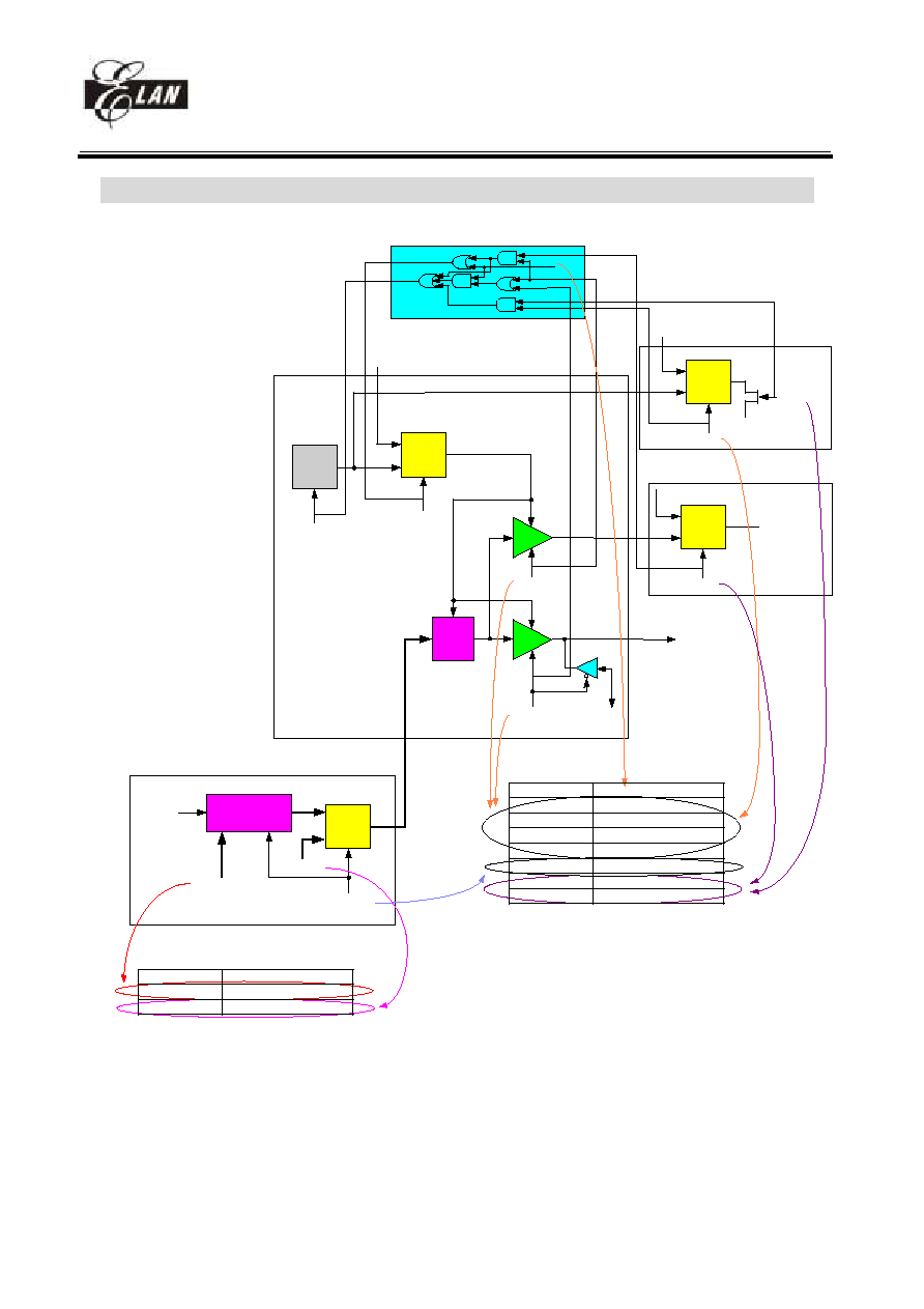
EM78P568
8-bit OTP Micro-controller
__________________________________________________________________________________________________________________________________________________________________
* This specification are subject to be changed without notice.
42
01/31/2004 V4.7
VII.9 Signal and control paths for DAC, DAC tone gen., CTCSS and Comparator
DAC Tone
Gen.
R-2R
fm =
447.829kHz
MUX
DA7~DA0
DAT/DAD
DAT7~DAT0
DAST/P67
PORT67
DAO/P67
DATEN
MUX
2.5V
ref
VDD
MUX
VDD
VRSEL
(part of Comparator)
MUX
ASW3
To ladder resistors
To Sub-Audio LPF
(part of CTCSS)
VTX3
VRX3
DAC
DAC Tone Gen.
B2
B1
CMPEN
Name
Register bit location
DAT7 ~ DAT0 RE PAGE1 bit 7 ~ 0
DA7 ~ DA0
RA PAGE1 bit 7 ~ 0
ASW3
DATEN
VREF
DAST/P67
CMPEN
VRSEL
REFSEL
REFEN
REFSEL
REFEN
Volgage reference control logic
Name
Register bit location
DAST/P67
IOCA PAGE1 bit 3
VRSEL
IOCA PAGE1 bit 4
DATEN
IOCA PAGE1 bit 5
VREF
IOCA PAGE1 bit 6
DAT/DAD
IOCA PAGE1 bit 7
CMPEN
IOC5 PAGE1 bit 7
ASW3
IOCE PAGE1 bit 2
ps. REFEN, REFSEL are not register bits.
Fig.16 Signal and control paths for analog circuit
The Fig.16 above try to explain how to use built-in 8-bit R-2R DAC. This DAC can be used as general DAC; here
is call "DAC general mode". Also it can be used as FRS CTCSS tone generation; here is called DAC tone generator
mode. When you use DAC general mode, you have to software program DAC input data DA7 ~ DA0 bits with
different points of value for tone generation. When you use DAC tone generator mode, you just need to set DAT7 ~
DAT0 bits and then the hardware "DAC Tone Gen." will auto-program DAC to generate corresponding frequency
signal output. Using this feature, it is easy and software free to generate accurate CTCSS tone.
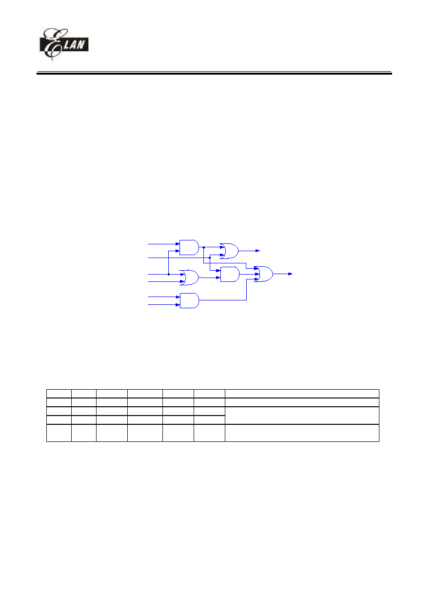
EM78P568
8-bit OTP Micro-controller
__________________________________________________________________________________________________________________________________________________________________
* This specification are subject to be changed without notice.
43
01/31/2004 V4.7
(1) DAC program mode
The below item "1" is for DAC general mode. The below item "2,3" are for DAC tone generator mode.
1. DAT/DAD = 0 DAC general mode, software-program DAC from DA7 ~ DA0 register bits , disable DAC
tone generator
2. DAT/DAD = 1 DAC tone generator mode, hardware-program DAC by setting DAT7 ~ DAT0 register
bits, enable DAC tone generator
3. DAT7 ~ DAT0 = 0 Disable DAC tone generator
(2) DAC output paths
DAST/P67 is used to enable DAC output buffer B1. DATEN is used to enable DAC output buffer B2.
1. ExternalDAC output from its output buffer B1 to DAO/P67 pin
DAST/P67 = 1 power on DAC, enable DAC output buffer B1, output sent to DAO/P67 pin
2. InternalDAC output from its output buffer B2 to CTCSS Sub-audio LPF
DATEN = 1 power on DAC, enable DAC output buffer B2, output sent to CTCSS VTX3
(3) Using 2.5V ref and DAC
ASW3
DATEN
VREF
DAST/P67
REFSEL
REFEN
CMPEN
VRSEL
Fig.17 Voltage reference control logic
"2.5V ref." is the reference voltage used in DAC, Comparator or CTCSS. The voltage reference control logic
process these combination use. For this reference used in Comparator, you just only take care of CMPEN and
VRSEL bits. For this reference used in others, you need to set ASW3, VREF, DATEN and DAST/P67. The
following table shows the least two bits setting to logic "1" (CMPEN=VRSEL=1 or ASW3=DATEN=1 or
VREF=DATEN=1 or VREF=DAST/P67=1) will "select 2.5V and enable 2.5V ref".
When REFSEL = 1, the 2.5V ref is select not VDD. (select 2.5V ref)
When REFEN = 1, the 2.5V ref is power on. (2.5V ref enable)
ASW3 VREF DATEN DAST/P67 CMPEN VRSEL Function
x
x
x
x
1
1
select 2.5V ref, enable 2.5V ref, enable Comparator
1
x
1
x
x
x
select 2.5V ref, enable 2.5V ref, enable DAC,
0
1
1
x
x
x
enable buffer B2, buffer B2 output to CTCSS LPF
x
1
0
1
x
x
select 2.5V ref, enable 2.5V ref, enable DAC,
enable buffer B1, buffer B1 output to DAO/P67 pin
(4) Select DAO/P67 pin as normal I/O P67
Set DAST/P67 = 0 to select normal I/O P67.
(5) Using DAC general mode
1. DAT/DAD = 0 select DAC general mode
2. Program DA7 ~ DA0
3. Enable DAC, enable DAC output buffer, select DAC reference source
(6) Using DAC tone generator mode
1. DAT/DAD = 1 select DAC tone generator mode
2. Program DAT7 ~ DAT0 = 1 to 255. (If DAT7 ~ DAT0 = 0, DAC tone gen. is disabled.)
3. Enable DAC, enable DAC output buffer, select DAC reference source
Ps. When DAC tone output is set to CTCSS Sub-audio LPF(ASW3=DATEN=1 or VREF=DATEN=1), it will be
forced to select 2.5V ref by voltage reference control logic. When its output is set to DAO/P67 pin, reference
voltage can be selected as VDD or 2.5V.
Ref to Page 18,19 for CTCSS tone generation table.
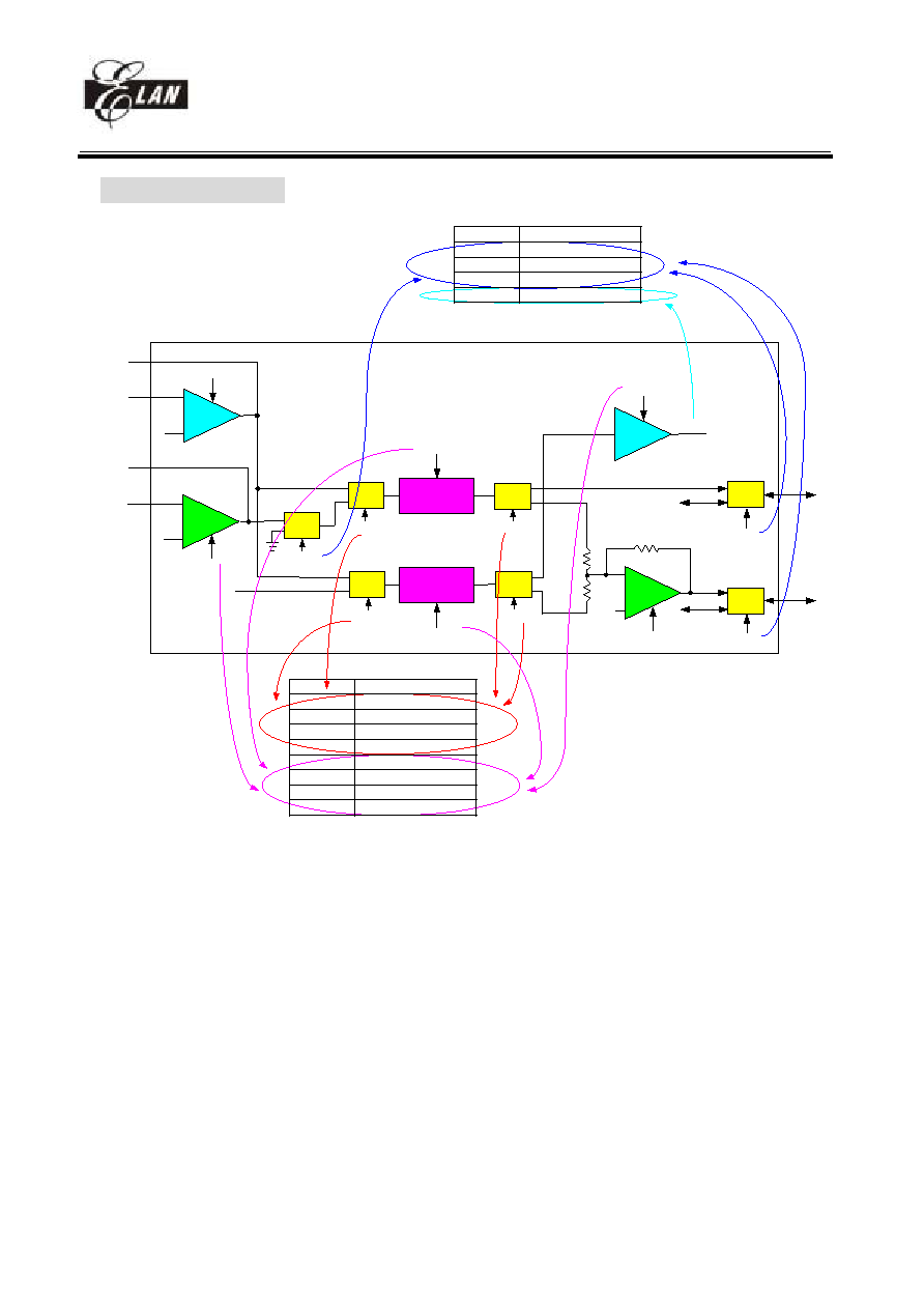
EM78P568
8-bit OTP Micro-controller
__________________________________________________________________________________________________________________________________________________________________
* This specification are subject to be changed without notice.
44
01/31/2004 V4.7
VII.10 CTCSS block
VII.10.1 Block control and signal flow description
Audio
BPF
VRF
VRF
Rx AMP
MIC AMP
Z C
AURX/P65
RXO
RXI
MICI
MICO
Summing
MTX/P66
VRF
-10dB
0dB
ASW1
ASW2
RXPWR
LPFPWR
BPFPWR
Sub-Audio
LPF
ASW4
MUX
PORT66
MTX
MUX
PORT65
AURX
P65S
P66S
AMP
MUX
ASW3
MUX
MUX
MUX
DETO
TXPWR
TXPWR
RXPWR
VRX1
VTX1
VRX2
VTX2
VRX3
VTX3
VRX4
VTX4
(from DAC output buffer B2)
CTCSS tone input
MUX
MICO
AMUTE
Name
Register bit location
ASW1
IOCE PAGE1 bit 0
ASW2
IOCE PAGE1 bit 1
ASW3
IOCE PAGE1 bit 2
ASW4
IOCE PAGE1 bit 3
LPFPWR
IOCE PAGE1 bit 4
BPFPWR
IOCE PAGE1 bit 5
RXPWR
IOCE PAGE1 bit 6
TXPWR
IOCE PAGE1 bit 7
Name
Register bit location
P65S
IOC6 PAGE1 bit 5
P66S
IOC6 PAGE1 bit 6
AMUTE
IOC6 PAGE1 bit 7
DETO
R7 PAGE1 bit 6
CTCSS block on page 36 Fig.14 is the key feature for FRS baseband signal processing. For receiving path, it
receives the RF demodulator output signal and extract the audio output signal to AURX pin. Also it decodes
CTCSS tone and its decoding data is shown in the DETO. For transmitting path, it combines audio signal from
Mic Amp and CTCSS signal from DAC tone generator(as description in VII.9 section) thru MTX output to RF
modulator input end. CTCSS block consists of amplifiers, analog switch, filters and zero-crossing detector
which descriptions are shown below.
RX AMP : (Receiving amplifier) It accepts RF demodulator output signals which combine demodulated
audio and CTCSS tone. Its bias voltage is VDD/2.
MIC AMP : (Microphone amplifier) It is the audio input amplifier. Its bias voltage is VDD/2.
MUX : (Analog multiplexer switch) It is used for analog signal path switching.
Audio BPF : (Audio band pass filter) This audio BPF has pass band 300Hz ~ 3.4kHz. It is used to let audio
signal pass through and filter out CTCSS tones. It plays an important role in extracting audio signal. Also it
cut out unwanted signal while audio signal transmitting.
Sub-Audio LPF : (Sub-audio low pass filter) This sub-audio LPF has pass band 253Hz. It is used to let
CTCSS tone pass through and filters out audio signal. It plays an important in extracting CTCSS tone. Also
it cut out unwanted signal while CTCSS tone transmitting.
Summing AMP : (Summing amplifier) It is an analog signal mixer for audio signal and CTCSS tone
transmitting. CTCSS tone will be attenuated about 10dB before signal mixing.
ZC : (Zero-crossing detector) This detector transforms CTCSS tone signal from analog form to digital form.
It will be the CTCSS tone detection.
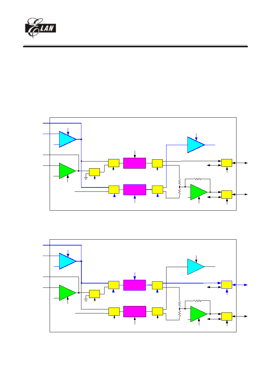
EM78P568
8-bit OTP Micro-controller
__________________________________________________________________________________________________________________________________________________________________
* This specification are subject to be changed without notice.
45
01/31/2004 V4.7
Description for register control bits
ASW1 ~ ASW4 for analog input/output signal path switching
RXPWR for power control of receiving RX AMP and ZC
TXPWR for power control of transmitting MIC AMP and Summing AMP
AMUTE for MIC AMP output signal muting
P65S for receiving audio output pin AURX or port P65 pin switching
P66S for transmitting output pin MTX or port P66 pin switching
The following is the above CTCSS block signal flow and it is easy to use these figures to explain how CTCSS
works. (`blue' highlight means signal flow and switch setting)
(1) RX : receiving CTCSS tone
Audio
BPF
VRF
VRF
Rx AMP
MIC AMP
Z C
AURX/P65
RXO
RXI
MICI
MICO
Summing
MTX/P66
VRF
-10dB
0dB
ASW1
ASW2
RXPWR = 1
LPFPWR = 1
BPFPWR
Sub-Audio
LPF
ASW4 = 0
MUX
PORT66
MTX
MUX
PORT65
AURX
P65S
P66S
AMP
MUX
ASW3 = 0
MUX
MUX
MUX
DETO
TXPWR
TXPWR
RXPWR =1
VRX1
VTX1
VRX2
VTX2
VRX3
VTX3
VRX4
VTX4
(from DAC output buffer B2)
CTCSS tone input
MUX
MICO
AMUTE
Fig.18
(2) RX : receiving audio
Audio
BPF
VRF
VRF
Rx AMP
MIC AMP
Z C
AURX/P65
RXO
RXI
MICI
MICO
Summing
MTX/P66
VRF
-10dB
0dB
ASW1 = 0
ASW2 = 0
RXPWR
LPFPWR
BPFPWR = 1
Sub-Audio
LPF
ASW4
MUX
PORT66
MTX
MUX
PORT65
AURX
P65S = 1
P66S
AMP
MUX
ASW3
MUX
MUX
MUX
DETO
TXPWR
TXPWR
VRX1
VTX1
VRX2
VTX2
VRX3
VTX3
VRX4
VTX4
(from DAC output buffer B2)
CTCSS tone input
MUX
MICO
AMUTE
RXPWR =1
Fig.19
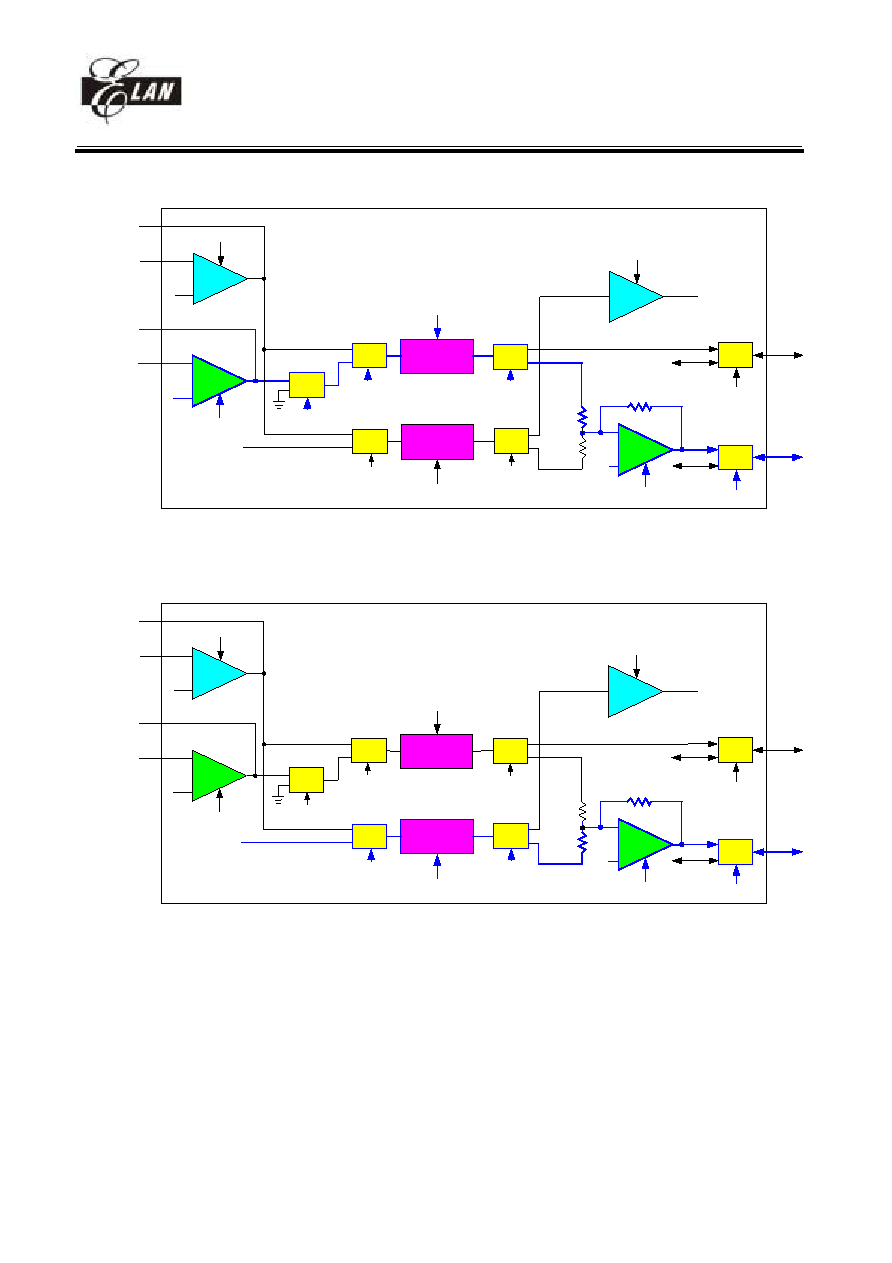
EM78P568
8-bit OTP Micro-controller
__________________________________________________________________________________________________________________________________________________________________
* This specification are subject to be changed without notice.
46
01/31/2004 V4.7
(3) TX : transmitting audio
Audio
BPF
VRF
VRF
Rx AMP
MIC AMP
Z C
AURX/P65
RXO
RXI
MICI
MICO
Summing
MTX/P66
VRF
-10dB
0dB
ASW1 = 1
ASW2 = 1
RXPWR
LPFPWR
BPFPWR = 1
Sub-Audio
LPF
ASW4
MUX
PORT66
MTX
MUX
PORT65
AURX
P65S
P66S = 1
AMP
MUX
ASW3
MUX
MUX
MUX
DETO
TXPWR = 1
TXPWR = 1
RXPWR
VRX1
VTX1
VRX2
VTX2
VRX3
VTX3
VRX4
VTX4
(from DAC output buffer B2)
CTCSS tone input
MUX
MICO
AMUTE = 0
Fig.20
(4) TX : transmitting CTCSS tone
Audio
BPF
VRF
VRF
Rx AMP
MIC AMP
Z C
AURX/P65
RXO
RXI
MICI
MICO
Summing
VRF
-10dB
0dB
ASW1
ASW2
RXPWR
LPFPWR = 1
BPFPWR
Sub-Audio
LPF
ASW4 = 1
MUX
PORT66
MTX
MUX
PORT65
AURX
P65S
P66S = 1
AMP
MUX
ASW3 = 1
MUX
MUX
MUX
DETO
TXPWR
TXPWR = 1
RXPWR
VRX1
VTX1
VRX2
VTX2
VRX3
VTX3
VRX4
VTX4
(from DAC output buffer B2)
CTCSS tone input
MUX
MICO
AMUTE
MTX/P66
Fig.21
VII.10.2 Special application on Audio/CTCSS tone mixing output
Generally speaking, users can use built-in DAC tone gen.(described in VII.9) to generate CTCSS
tone accompanied with audio on MTX/P66 pin output without problem. For some customers, due to
modulation index criteria of their FM modulator cannot accept built-in CTCSS tone because this level is
too large for them to use.
In this case, there are two ways to solve this problem :
(1) One way is not to use built-in DAC tone gen. but need to program built-in DAC to generate CTCSS
tone by user software algorithm. User software algorithm can normalize the final CTCSS tone level
to their requirement without adding any external elements.
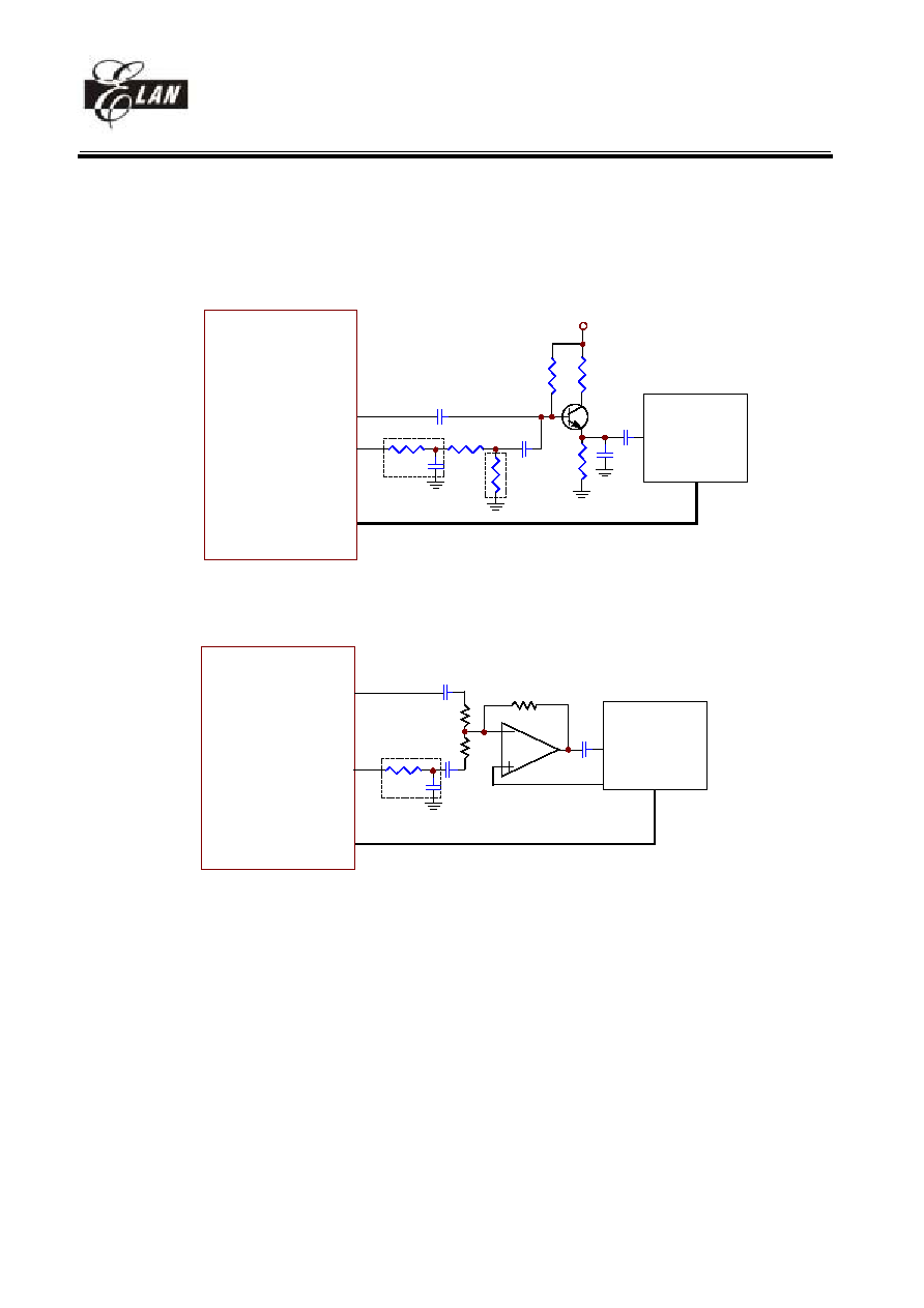
EM78P568
8-bit OTP Micro-controller
__________________________________________________________________________________________________________________________________________________________________
* This specification are subject to be changed without notice.
47
01/31/2004 V4.7
(2) The other way is still to use built-in DAC tone gen. but need some external element to attenuate
CTCSS tone on DAO/P67 pin. Program some control bit to let CTCSS output on DAO/P67 pin refer
to VII.9 (3) description). Because DAO/P67 output is stair-case waveform, we need put simple RC
LPF circuit to smooth output waveform before CTCSS attenuation circuit. Also RC LPF has some
attenuation effect. It depends on its cut-off frequency of LPF. User can design by his own way.
There are two suggestion circuits for your reference as following.
MTX/P66
DAO/P67 31
32
FM
modulator
(I/O port)
VCC
(option)
(LPF for DA sample clk)
MTX/P66
DAO/P67
32
FM
modulator
(I/O port)
(bias)
31
(LPF for DA sample clk)
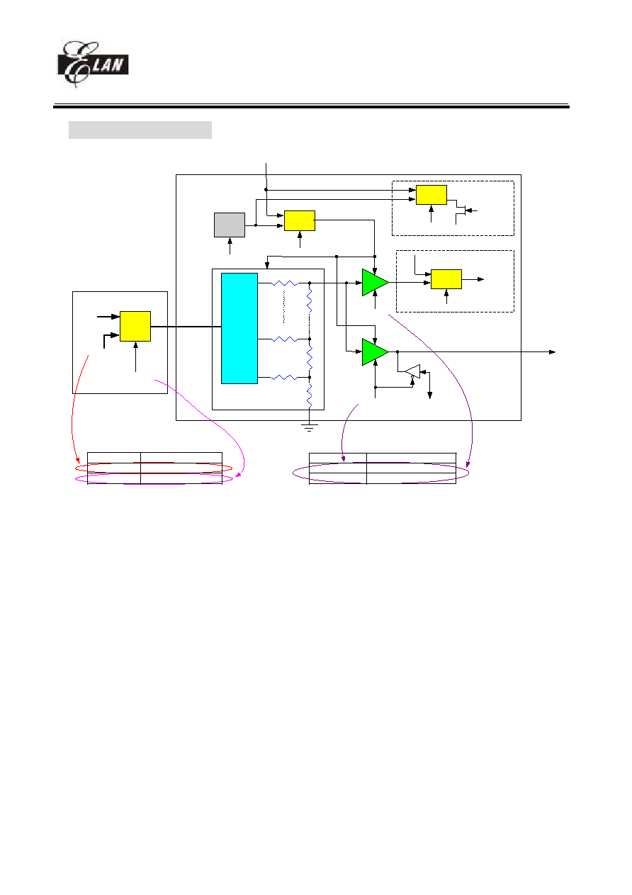
EM78P568
8-bit OTP Micro-controller
__________________________________________________________________________________________________________________________________________________________________
* This specification are subject to be changed without notice.
48
01/31/2004 V4.7
VII.11 8-bit R-2R DAC
DAST/P67
PORT67
DAO/P67
DATEN
MUX
2.5V
ref
VDD
REFSEL
REFEN
B2
B1
2R
2R
R
2R
2R
R
8-bit
DAC
input
data
buffer
(This circuit is from Comparator)
VRSEL
To ladder resistors
CMPEN
(This circuit is from CTCSS)
MUX
ASW3
VTX3
VRX3
To Sub-Audio LPF
MUX
DAC input
MUX
DA7~DA0
DAT/DAD
(part of DAC Tone Gen.)
DAC tone gen
Name
Register bit location
DA7 ~ DA0
RA PAGE1 bit 7 ~ 0
DAT/DAD
IOCA PAGE1 bit 7
Name
Register bit location
DAST/P67
IOCA PAGE1 bit 3
DATEN
IOCA PAGE1 bit 5
ps. Please refer to "Voltage reference control logic" to set DAC reference.
Fig.22 DAC block
In DAC tone generator mode, user can get CTCSS tone output. In other case, DAC is useful in general tone
generation such as key tone, alert tone, music and so on. In DAC general mode, only VREF and DAST/P67 bits are
relative to DAC reference voltage. DAC reference voltage is come from VDD or 2.5V ref. Setting VREF bit (IOCE
PAGE1 bit 6) = 0/1 to select VDD/2.5V as reference. Setting DAST/P67 bit = 1 to power on DAC and also enable
output buffer B1. After that, DAC output signal will be sent to DAO/P67 pin.
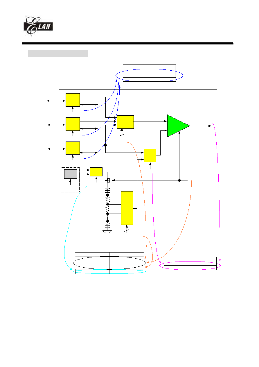
EM78P568
8-bit OTP Micro-controller
__________________________________________________________________________________________________________________________________________________________________
* This specification are subject to be changed without notice.
49
01/31/2004 V4.7
VII.12 4-bit Comparator
PORT62
MUX
CMP1
P62S
PORT63
MUX
CMP2
P63S
PORT64
MUX
CMP3
P64S
MUX
CMPS1
CMPS0
+
-
MUX
CMPREF
CMPFLAG
CMPEN
0
1
2
CMP1/P62
CMP2/P63
CMP3/P64
MUX
1/2R
R
R
1/2R
5
CMP_B4 to CMP_B0
11111
11110
00000
VRSEL
MUX
2.5V
ref
2.5V
REFEN
(This ckt is form DAC)
VR
VDD
Name
Register bit location
CMPEN
IOC5 PAGE1 bit 7
CMPS1 ~ CMPS0
IOC5 PAGE1 bit 6 ~ 5
CMP_B4 ~ CMP_B0 IOC5 PAGE1 bit 4 ~ 0
Name
Register bit location
CMPREF
RA PAGE0 bit 1
CMPFLAG
RA PAGE0 bit 2
Name
Register bit location
P62S
IOC6 PAGE1 bit 2
P63S
IOC6 PAGE1 bit 3
P64S
IOC6 PAGE1 bit 4
VRSEL
IOCA PAGE1 bit 4
This comparator is not only a single comparator. It consists of 16-R resistor string, 3-channel input and optional
external comparison reference source input. The 16-R resistor string acts as 16-level voltage divider which top
voltage reference can be selected from VDD or 2.5V ref. Use above register bits to set the whole job. This
comparator is used to some applications such as voltage detection, RSSI level, sensor output level and other slow
signal level transition detection and so on. This comparator can be called a simple 4-bit low speed ADC but the
sampling time is decided by software. For AC frequency detection, it is limited by it output comparator structure.
We suggest the detected AC frequency below 1kHz.
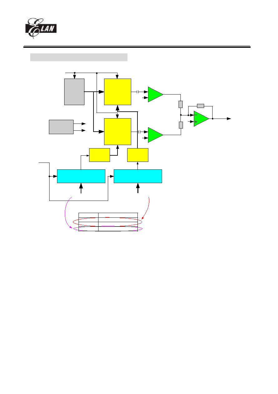
EM78P568
8-bit OTP Micro-controller
__________________________________________________________________________________________________________________________________________________________________
* This specification are subject to be changed without notice.
50
01/31/2004 V4.7
VII.13 Programming tone generators
N-R
resistor
string
Tone 1
analog
multiplexer
Tone 2
analog
multiplexer
Tone 2
programmable counter
Tone 1
programmable counter
TONE
Buffer
Buffer
Mixer
fi
fs2
T2Mux
control
T1Mux
control
fs1
(output inverse)
Vref2
Vref2
Vref2
Reference
voltage
Vref1
Vref1
Vref2
VT
fs1 = fi / N1, fs2 = fi / N2
N2
N1
fT1 = fi / N1 / N, tone1 output frequency
fT2 = fi / N2 / N, tone2 output frequency
T27 ~ T20
T1A ~ T10
Name
Register bit location
T1A ~ T18 IOCE PAGE0 bit 2 ~ 0
T17 ~ T10 IOCD PAGE0 bit 7 ~ 0
T27 ~ T20 IOCA PAGE0 bit 7 ~ 0
Fig.23 Programming tone generator
Programming tone generators is an universal dual tone generators. It includes Tone 1 and Tone 2 generators which
can be combines as dual tones output or either one tone output. The clock source fi is come from PLL and divided
to required ratio. Tone 1 and Tone 2 are sinewave output. The programming tone generators consists of Tone 1/2
programmable counters, analog multiplexer, N-R resistor string, output buffers, mixer amplifier and reference
voltage. N-R resistor is a voltage divider which has different output levels. By programmable counters and analog
multiplexer, the hardware will automatically generate individual divider output with circular order back and forth.
The output frequency will be 119957/N1 for Tone 1 and 11.957/N2 for Tone 2, where N1 is 11-bit T1A ~ T10 and
N2 is 8-bit T17 ~ T10.
EM78P568
8-bit OTP Micro-controller
__________________________________________________________________________________________________________________________________________________________________
* This specification are subject to be changed without notice.
51
01/31/2004 V4.7
VIII. Absolute Operation Maximum Ratings
RATING SYMBOL
VALUE
UNIT
DC SUPPLY VOLTAGE
VDD
-0.3 To 6
V
INPUT VOLTAGE
Vin
-0.5 to VDD +0.5
V
OPERATING TEMPERATURE RANGE
Ta
-30 to 70
IX. DC Electrical Characteristic
(Ta = 0
°C ~ 70°C, AVDD=VDD=5V±5%, VSS=0V)
Parameter Symbol
Condition Min
Typ
Max
Unit
Input leakage current for
input pins
IIL1
VIN = VDD, VSS
±1
µA
Input leakage current for bi-
directional pins
IIL2
VIN = VDD, VSS
±1
µA
Input high voltage
VIH
2.5
V
Input low voltage
VIL
0.8
V
Input high threshold voltage
VIHT
/RESET, TCC
2.0
V
Input low threshold voltage
VILT
/RESET, TCC
0.8
V
Clock input high voltage
VIHX
OSCI
3.5
V
Clock input low voltage
VILX
OSCI
1.5
V
Output high voltage for
PORT6,7,8,B
VOH1 IOH = -5mA
2.4
V
Output high voltage for
PORT9
VOH2 IOH = -14mA
2.4
V
Output low voltage for
PORT6,7,8,B
VOL1 IOH = 5mA
0.4
V
Output low voltage for
PORT9
VOL2 IOH = 10mA
0.4
V
LCD drive reference voltage
VLCD VDD=5V, Contrast adjust
4 ~ 5
V
Pull-high current
IPH
Pull-high active input pin at
VSS
-10
-15
µA
Power down current
(SLEEP mode)
ISB1
All input and I/O pin at VDD,
output pin floating, WDT
disabled
1 5
µA
Low clock current
(GREEN mode)
ISB2
CLK=32.768KHz, All analog
circuits disabled, All input
and I/O pin at VDD, output
35
50
µA
Low clock current
(IDLE mode)
ISB3
CLK=32.768KHz, All analog
circuits disabled, All input
and I/O pin at VDD, output
30
45
µA
Operating supply current
(Normal mode)
ICC1 /RESET=High,
CLK=3.582MHz, All analog
circuits disabled, output pin
floating
1 2 mA
Tone generator reference
voltage
Vref2
VREG is regulator output
0.5
0.7
VREG
Tone1 signal strength
V1rms Root mean square voltage
130
155
180
mV
Tone2 signal strength
V2rms Root mean square voltage
1.259V1rms
mV
EM78P568
8-bit OTP Micro-controller
__________________________________________________________________________________________________________________________________________________________________
* This specification are subject to be changed without notice.
52
01/31/2004 V4.7
2.5Vref for Comparator or DAC
Parameter Symbol
Condition
Min
Typ
Max
Unit
Internal 2.5V ref. voltage.
2.5VREF
VDD=5V, 25 deg
2.14 2.32 2.44
V
VDD=3V, 25 deg
2.04 2.25 2.36
V
Reference voltage linearity
2.5
V
REF
/
V
DD
VDD=5.5V ~ 3.0V
, 25 deg
5 8 %
VDD=3.0V ~ 2.7V
, 25 deg
8 15 %
Effective VDD reference for Comparator or DAC
Parameter Symbol
Condition
Min
Typ
Max
Unit
VDD ref. voltage.
VDDref
VDD=5V ~ 2.7V,
, - 20 ~ +50 deg
VDD-
0.05
VDD-
0.02
VDD V
(Operation current consumption for analog circuit) (Ta = 0
°C ~ 70°C, AVDD=VDD=5V±5%, VSS=0V)
Parameter Symbol
Condition Min
Typ
Max
Unit
Programming tone generators
Operation current for
Programming tone
generators
I_TONE TONE1 is power on
TONE2 is power on
0.35
0.6 mA
Digital to analog converter
Operation current for DAC
I_DA
0.65
0.9 mA
Comparator
Operation current for
Comparator
I_CMP
70 120 uA
CTCSS
Operation current for RX
power on
I_RX RXPWR=1,
TXPWR=0
LPFPWR=0, BPFPWR=0
0.7
1.0 mA
Operation current for TX
power on
I_TX RXPWR=0,
TXPWR=1
LPFPWR=0, BPFPWR=0
0.12
0.2 mA
Operation current for LPF
power on
I_LPF RXPWR=0,
TXPWR=0
LPFPWR=1, BPFPWR=0
0.3
0.5 mA
Operation current for BPF
power on
I_BPF RXPWR=0,
TXPWR=0
LPFPWR=0, BPFPWR=1
0.3
0.5 mA
* the spec for above table not including MCU current consumption
XI. AC Electrical Characteristic
CPU instruction timing (Ta = -30
°C ~ 70°C, AVDD=VDD=5V, VSS=0V)
Parameter Symbol
Condition
Min
Typ
Max
Unit
Input CLK duty cycle
Dclk
45
50
55
%
Instruction cycle time
Tins
32.768kHz
3.582MHz
60
550
us
ns
Device delay hold time
Tdrh
16
ms
TCC input period
Ttcc
Note 1
(Tins+20)/N
ns
Watchdog timer period
Twdt
Ta = 25
°C
16
ms
Note 1: N= selected prescaler ratio.
EM78P568
8-bit OTP Micro-controller
__________________________________________________________________________________________________________________________________________________________________
* This specification are subject to be changed without notice.
53
01/31/2004 V4.7
OSC and reset timing characteristics (see Fig.25 for details)
Description
Symbol Min Typ Max Unit
Oscillator timing characteristic
OSC start up
32.768kHz
Toscs
400
1500
ms
3.579MHz
PLL
5
10
us
Reset timing characteristic
The minimum width of reset low pulse
Trst
3
uS
The delay between reset and program start
Tdrs
18
mS
Embedded LCD driver
Symbol Parameter
Condition
Min Typ Max
Unit
Frame
LCD frame frequency
1/8, 1/16 duty
64
Hz
TONE generators for AC Characteristic (AVDD=VDD=5V,Ta=+25
°C)
CHARACTERISTIC Min
Typ
Max Unit
Tone1/Tone2 signal strength (root mean square voltage)
Tone1 signal strength V1rms (ps1) ~= -14dBm (600)
130
155
180
mV
Tone2 signal strength V2rms (ps1) ~ = -12dBm (600)
1.259V1rms mV
Tone twist
(Tone1 Tone2) twist
-2
dB
(ps1) : V1rms and V2rms has 2 dB difference. It means 20log(V2rms/V1rms) = 20log1.259 = 2 (dB)
CTCSS block (AVDD=VDD=5V,Ta=+25
°C)
Parameter Min. Typ. Max. Unit
RX mode
Zero crossing threshold (mVrms) (note : 1*)
20
mV
Data Duty Ratio
30
50
70
%
TX mode
CTCSS tone (form Tone 2) to VTX3, for 600
-12
dBm
CTCSS tone to MTX, for 600
-22
dBm
Filter
BPF for Audio
Pass-Band Frequency
300
3400
Hz
Pass-Band Ripple
1.0
dB
LPF for Sub-Audio
Pass-Band Frequency
60
253
Hz
Pass-Band Ripple
1.0
dB
Output
Driving capacity for AURX pin
30
uA
Driving capacity for MTX pin
30
uA
Output loading impedance for AURX pin
(Ref. Voltage = 2.5V)
42
k
Output loading impedance for MTX pin
(Ref. Voltage = 2.5V)
42
k
Note :
1*. Test under Fig.26 application circuit. Zero crossing threshold means ZC's transition level in Fig.14 CTCSS
block. This level is close but not equal to CTCSS receiving sensitivity. The CTCSS receiving sensitivity
partially depends on user software judgement. Also CTCSS receiving sensitivity can be adjusted by changing
external resistors of RX AMP in Fig.26 application circuit.
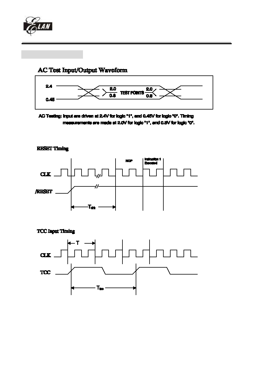
EM78P568
8-bit OTP Micro-controller
__________________________________________________________________________________________________________________________________________________________________
* This specification are subject to be changed without notice.
54
01/31/2004 V4.7
XII. Timing Diagrams
Fig.24 AC timing
ins
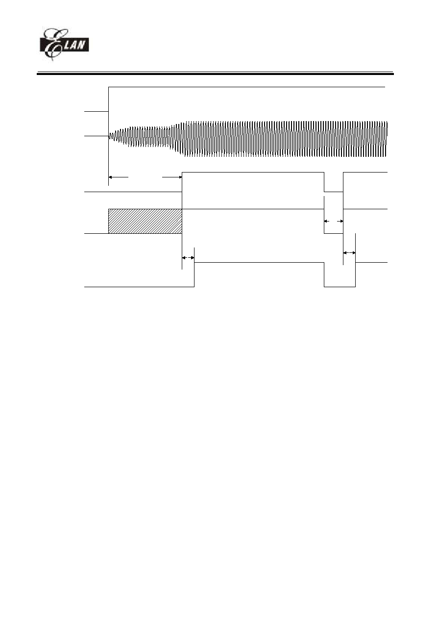
EM78P568
8-bit OTP Micro-controller
__________________________________________________________________________________________________________________________________________________________________
* This specification are subject to be changed without notice.
55
01/31/2004 V4.7
VDD
OSC
Power
on reset
/RESET
Tdrs
Toscs
Program
Active
Tdrs
Trst
Fig.25 OSC and reset timing
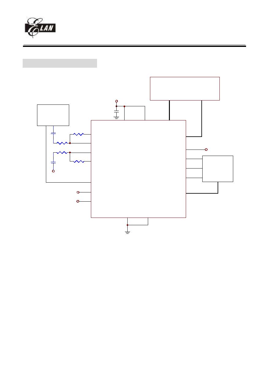
EM78P568
8-bit OTP Micro-controller
__________________________________________________________________________________________________________________________________________________________________
* This specification are subject to be changed without notice.
56
01/31/2004 V4.7
XIII. Application circuits
AVDD
RXO
22
MTX/P66 32
AURX/P65 33
VDD
VCC
21
51
RXI
23
100k
100k
0.1u
from Mic
MICI
26
MICO
27
100k
100k
0.1u
CMP1/P62
36
CMP2/P63
35
CMP3/P64
34
low battery detect
RSSI
(other detect)
30
44
AVSS
VSS
LCD display
COM(0..3)
SEG(0..19)
to speaker AMP
DAO/P67 31
TONE 28
FM
modulator
FM
demodulator
(I/O port)
EM78P568
14..11
10,100..82
Fig.26 Application circuit for FRS