
EM78P813
8-BIT OTP MICRO-CONTROLLER
ELAN MICROELECTRONICS CORP.
No. 12, Innovation 1
st
RD., Science-Based Industrial Park
Hsin Chu City, Taiwan, R.O.C.
TEL: (03) 5639977
FAX: (03) 5630118
Version 1.6
EM78P813
8-bit OTP Micro-controller
__________________________________________________________________________________________________________________________________________________________________
* This specification is subject to change without notice.
2
2004/8/19 (V1.6)
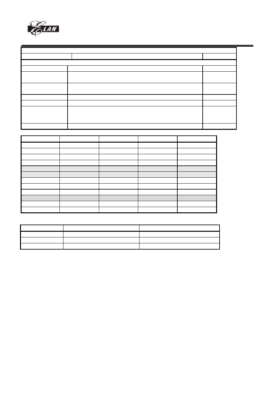
Specification Revision History
Version Content
EM78813 ICE
1.0 Initial
version
1.1
Add "VNWSB" pin
Add touch panel pen press / unpress detection
2002/12/25
1.2 Remove
"VNWSB"
pin
Change FSK, DTMF and CW power control
2003/3/4
1.3
Modify Current DA resolution from 7 bits to 10 bits
2003/3/26
1.4
Add 208 pin QFP package
2003/9/1
1.5
1. Modify normal mode operation voltage
2. Modify DC electrical characteristic
3. Remove AD and Touch panel function
2003/12/3
1.6 Remove
Idle
mode
2004/8/19
EM78R813 EM78P813 EM78813 EM78815
Data RAM
16K X 8
16K X 8
4K X 8
4K X 8
PRG ROM
64K X 13
64K X 13
48K X 13
64K X 13
DATA ROM
256K X 8
256K X 8
256K X 8
256K X 8
Expand ROM
2M X 8
2M X 8
--
2M X 8
STACK
32
24
24
24
Common RAM
256 byte
128 byte
128 byte
128 byte
OP O X X X
Current
DA
O O O O
DED input
Share with TIP
Independent pin
Independent pin
Independent pin
Key scan
Chipsel pin decide Chipsel pin decide
Share with SEG
Share with IO
Pin 256 186 184 105
Process
.5 .5 .5 .35
EM78813/EM78815 mode select
EM78813 mode(IOCB page1 bit6=0) EM78815 mode(IOCB page1 bit6=1)
KEY strobe pin
Share with SEG50~SEG65
Share with PORT8 and PORT9
Internal LCD driver Enable
Disable(COM,SEG pin high impedance)
Expand function
NO
Interface share with SEG34~SEG65
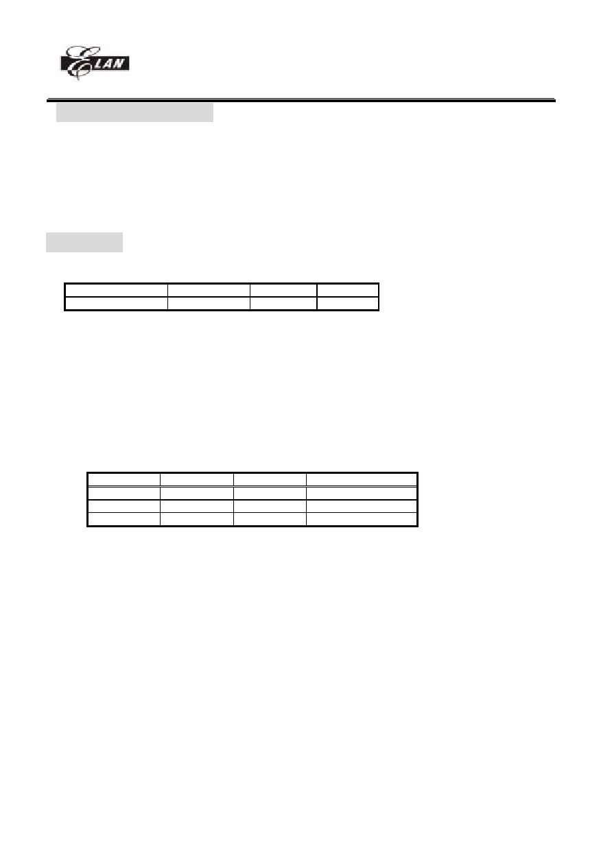
Application Note
1. 2.0V reference voltage will power down when both RD PAGE2 bit7(DAREF) and RA PAGE2 bit7(CMPEN) are clear
to 0.
2. For targeting interrupt and program run to address 0x0008, ACC, R3(STATUS), R5(Program page) and R4(6,7) will
be automatically saved and R3(6,7) R register page will set to PAGE0, and reload after the instruction "RETI".
3. Before using Key tone function, please set Port 76 as output type.
4. In EM78R813, pin EGIN1 and EGIN2 are shared with pin TIP and RIN, but they are independent in EM78P813 and
EM78813.
5. In EM78R813, user can turn on one of FSK, DTMF and CW power at the same time. In OTP and mask version, user
can turn on both CID(one of FSK and DRMF) or CW power at the same time, but FSK and DTMF power can not turn
on simultaneously.
6. Please do not switch MCU operation mode from normal mode to sleep mode directly. Before into sleep mode, please
switch MCU to green mode.
7.For accessing data ROM,EM78P813 (OTP) can work at 10.74MHz, but please note that ROM type EM78813 only can
work at 5.37MHz
8. While switching main clock (regardless of high freq to low freq or on the other hand), adding 6 instructions delay (NOP)
is required.
EM78P813
8-bit OTP Micro-controller
__________________________________________________________________________________________________________________________________________________________________
* This specification is subject to change without notice.
3
2004/8/19 (V1.6)
I. General Description
The EM78P813 is an 8-bit CID (Call Identification) RISC type microprocessor with low power, high speed
CMOS technology. There are 64Kx13 bits and 256Kx8 bits Electrical One Time Programmable Read Only Memory
(OTP-ROM) within it. It provides security bits and some One time programmable Option bits to protect the OTP
memory code from any external access as well as to meet user's options.
Integrated onto a single chip are on chip watchdog (WDT), programmable real time clock/counter,
external/internal interrupt, power down mode, LCD driver, FSK decoder, Call waiting decoder, Energy Detector (DED) ,
DTMF receiver, Programming Tone generator, build-in KEY TONE clock generation, Comparator and tri-state I/O. The
EM78P813 provides a single chip solution to design a CID of calling message display.
II. Feature
CPU
�
Operating voltage : 2.2V~5.5V at main CLK less then 3.58MHz.
Main CLK(Hz)
Under 3.58M
5.37M
10.74M
Operating Voltage(min)
2.2
2.5
3
�
64K�13 Program ROM
�
256K�8 data ROM
�
16K�8 data RAM
�
128�8 common register
�
Up to 56 bi-directional tri-state I/O ports (32 shared with LCD Segment pins)
�
IO with internal Pull high, wake-up and interrupt functions
�
STACK: 24 level stack for subroutine nesting
�
TCC: 8-bit real time clock/counter (TCC) with 8-bit prescaler
�
COUNTER1: 8 or 16 bit counter with 8-bit prescaler can be an interrupt source
�
COUNTER2: 8-bit counter with 8-bit prescaler can be an interrupt source
�
Watch Dog : Programmable free running on chip watchdog timer
�
CPU modes:
Mode
CPU status
Main clock
32.768kHz clock status
Sleep mode
Turn off
Turn off
Turn off
Green mode
Turn on
Turn off
Turn on
Normal mode
Turn on
Turn on
Turn on
�
4 step Normal mode CLK : 1.79 , 3.58 , 5.37 , 10.74 MHz generated by internal PLL.
�
13 interrupt source , 8 external , 5 internal
�
Key Scan : Port key scan function up to 16x4 keys
�
Sub-Clock: 32.768KHz crystal.
�
Key tone output :4KHz, 2KHz ,1KHz (shared with IO)
�
Comparator: 3-channel comparators: internal (16 level) or external reference voltage. (shared with
IO)
Serial transmitter/receiver interface
�
Serial Peripheral Interface (SPI): Interrupt flag available for the read buffer full, Programmable baud rates of
communication, Three-wire synchronous communication. (shared with IO)
Current D/A
�
Operation Voltage : 2.5V5.5V
�
10-bit resolution and 3-bit output level control
�
Current DA output can drive speaker through a transistor for sound playing. (shared with IO)
Programmable Tone Generators
�
Operation Voltage 2.2V5.5V
�
Programmable Tone1 and Tone2 generators
�
Independent single tone generation for Tone1 and Tone2

EM78P813
8-bit OTP Micro-controller
__________________________________________________________________________________________________________________________________________________________________
* This specification is subject to change without notice.
4
2004/8/19 (V1.6)
�
Mixed dual tone generation by Tone1 and Tone2 with 2dB difference
�
Can be programmed for DTMF tone generation
�
Can be programmed for FSK signal (Bell202 or V.23) generation
CID
�
Operation Voltage 2.7V5.5V for FSK
�
Operation Voltage 2.7V5.5V for DTMF receiver
�
Compatible with Bellcore GR-30-CORE (formerly as TR-NWT-000030)
�
Compatible with British Telecom (BT) SIN227 & SIN242
�
FSK demodulator for Bell 202 and ITU-T V.23 (formerly as CCITT V.23)
�
Differential Energy Detector (DED) for line energy detection
CALL WAITING
�
Operation Voltage 2.6V5.5V
�
Compatible with Bellcore special report SR-TSV-002476
�
Call-Waiting (2130Hz plus 2750Hz) Alert Signal Detector
�
Good talkdown and talkoff performance
�
Sensitivity compensated by adjusting input OP gain
LCD (16x112 , 24x106 , 32x98 )
�
Operating Voltage range:
Supply voltage : 2.5V to 5.5V
Through charge pump circuit and regulate adjusting, LCD device voltage : 3.6V to 5.3V
�
Maximum common driver pins : 16/24/32
�
Maximum segment driver pins : 112(SEG0..SEG111)/106(SEG0..SEG105)/ 106(SEG0..SEG97)
�
Shared COM16 ~ COM23 pins with SEG113 ~ SEG106 pins
�
Shared COM24 ~ COM31 pins with SEG105 ~ SEG98 pins
�
1/5 bias for 16 common mode , 1/6 bias for 24 common mode and 1/7 for 32 common mode
�
1/16, 1/24, 1/32 duty
�
32 Level LCD contrast control (software)
�
Internal resistor circuit for LCD bias.
External LCD controller (64 x 256 dot MAX for a pair of Master and Slave LCD Driver)
�
Multi-chip operation(Master, Slave) available for external LCD device.
Expand
�
128K Program ROM (64K on_chip and provided Parallel transmitter interface for 64K external
program ROM access.)Through external address & data bus, 2M byte Data ROM can be addressing.
Package type
�
186 pin die : EM78P813H
�
208 pin QFP : EM78P813AQ(POVD disable)
EM78P813BQ(POVD enable)
III. Application
�
adjunct units
�
SMS phones
�
feature phones

EM78P813
8-bit OTP Micro-controller
__________________________________________________________________________________________________________________________________________________________________
* This specification is subject to change without notice.
5
2004/8/19 (V1.6)
IV. Pin Configuration
COM9
COM8
COM7
COM6
COM5
COM4
COM3
COM2
COM1
COM0
VC4
VC3
VC2
VC1
VDD
XI
N
XO
UT
PLLC
TONE
TIP
RING
AVSS
/RE
S
E
T
P7
0
/
I
N
T
0
P7
1
/
I
N
T
1
P7
2
/
I
N
T
2
P7
3
/
I
N
T
3
P7
4
/
I
N
T
4
P7
5
/
I
N
T
5
P
7
6/
I
N
T6
/KT
ONE
P7
7
/
I
N
T
7
P60/STGT
P61/EST
P62
P63
P64
P65/CMP1
P66CMP2
P67CMP3
PD5/SDO
SEG82/PB0/LD0
SEG83/PB1/LD1
SE
G
8
4
/
P
B
2
/
L
D
2
SE
G
8
5
/
P
B
3
/
L
D
3
SE
G
8
6
/
P
B
4
/
L
D
4
SE
G
8
7
/
PB
5
/
L
D
5
SE
G
8
8
/
PB
6
/
L
D
6
SEG8
9/P
B
7
/
L
D
7
SE
G
9
0
/
PC0
/
CS
2
SEG9
1/P
C
1
/
C
S
1
SE
G
9
2
/
PC2
/
W
R
SEG66/P80
SEG67/P81
SEG68/P82
SEG69/P83
SEG70/P84
SEG71/P85
SEG72/P86
SEG73/P87
SEG74/P90
SEG75/P91
SEG76P92
SEG77/P93
SEG78/P94
SEG79/P95
SE
G
3
3
SE
G
3
2
SE
G
3
1
SE
G
3
0
SE
G
2
9
SEG2
8
SEG2
7
SEG2
6
SEG2
5
SEG2
4
SEG2
3
SEG2
2
SEG2
1
SEG2
0
SEG1
9
SEG1
8
SEG1
7
SEG1
6
SEG1
5
SEG1
4
SEG1
3
SEG1
2
SEG1
1
SE
G
1
0
SEG9
SE
G
8
COM13
COM12
COM11
COM10
1
2
3
4
5
6
7
8
9
10
11
12
13
14
15
16
17
18
19
20
21
22
23
24
25
26
27
28
29
30
31
32
33
34
35
36
37
38
39
40
41
42
43
44
45
46 47
48 49
50
51
52 53
54
55
56 57 58 59 60
63
64 65
66 67 68
69
70 71
72
136
137
13
8
15
2
15
3
15
4
15
5
15
6
15
7
15
8
15
9
16
0
16
1
16
2
16
3
16
4
13
9
14
0
14
1
14
2
14
3
14
4
14
5
14
6
14
7
14
8
14
9
15
0
15
1
CWGS
CWIN
VC5
16
5
16
6
16
7
16
8
16
9
17
0
17
1
17
2
17
3
17
4
17
5
17
6
17
7
AVDD
Vout
VREF
C1
C2
COM14
COM15
SE
G
1
SEG0
SE
G
3
SE
G
2
SE
G
5
SE
G
4
SE
G
7
SE
G
6
SEG80/P96
SEG81/P97
SE
G
9
3
/
P
C
3
/
RD
SEG9
4/P
C
4
/
A
0
SEG9
5/P
C
5
SE
G
9
6
/
P
C
6
SE
G
9
7
/
P
C
7
CO
M
3
1/
SE
G
9
8
CO
M
3
0/
SE
G
9
9
CO
M
2
9/
SE
G
1
0
0
CO
M2
8/S
E
G
1
01
CO
M2
7/S
E
G
1
02
CO
M2
6/S
E
G
1
03
CO
M2
5/S
E
G
1
04
CO
M2
4/S
E
G
1
05
COM23/
SEG106
COM22/
SEG107
COM21/
SEG108
COM20/
SEG109
COM19/
SEG110
CO
M
1
8
/
SE
G
1
11
COM17
CO
M
1
6
PD0
PD1
PD2
PD3
PD4/SCK
LVSS
LVDD
PD6/SDI
PD7/DAOUT
EGIN1
EGIN2
73 74 75 76
77
78 79
80
81 82
83 84 85 86 87
88 89
90
101
100
99
98
97
96
95
94
93
92
91
110
109
108
107
106
105
104
103
102
119
118
117
116
115
114
113
112
111
128
127
126
125
124
123
122
121
120
135
134
133
132
131
130
129
17
8
17
9
18
0
18
1
61 62
GN
D
TEST
18
2
18
3
EX
S
E
L
CH
I
P
S
E
L
SEG57/RD
SEG58/EXD7
SEG59/EXD6
SEG61/EXD4
SEG60/EXD5
SEG62/EXD3
SEG63/EXD2
SEG64/EXD1
SEG65/EXD0
SE
G
4
5
/
E
X
A
9
S
E
G
44/EX
A
1
0
S
E
G
43/EX
A
1
1
SEG54/EXA0
SEG53/EXA1
SEG52/EXA2
SEG51/EXA3
SEG50/EXA4
S
E
G
4
9/
E
XA5
S
E
G
4
8/
E
XA6
SE
G
4
7
/
E
X
A
7
SE
G
4
6
/
E
X
A
8
SEG56/WR
SEG55/CS
S
E
G
42/EX
A
1
2
S
E
G
41/EX
A
1
3
S
E
G
40/EX
A
1
4
S
E
G
39/EX
A
1
5
S
E
G
38/EX
A
1
6
S
E
G
37/EX
A
1
7
S
E
G
36/EX
A
1
8
S
E
G
35/EX
A
1
9
S
E
G
34/EX
A
2
0
POVD
POVD
VD
D
18
4
18
5
18
6
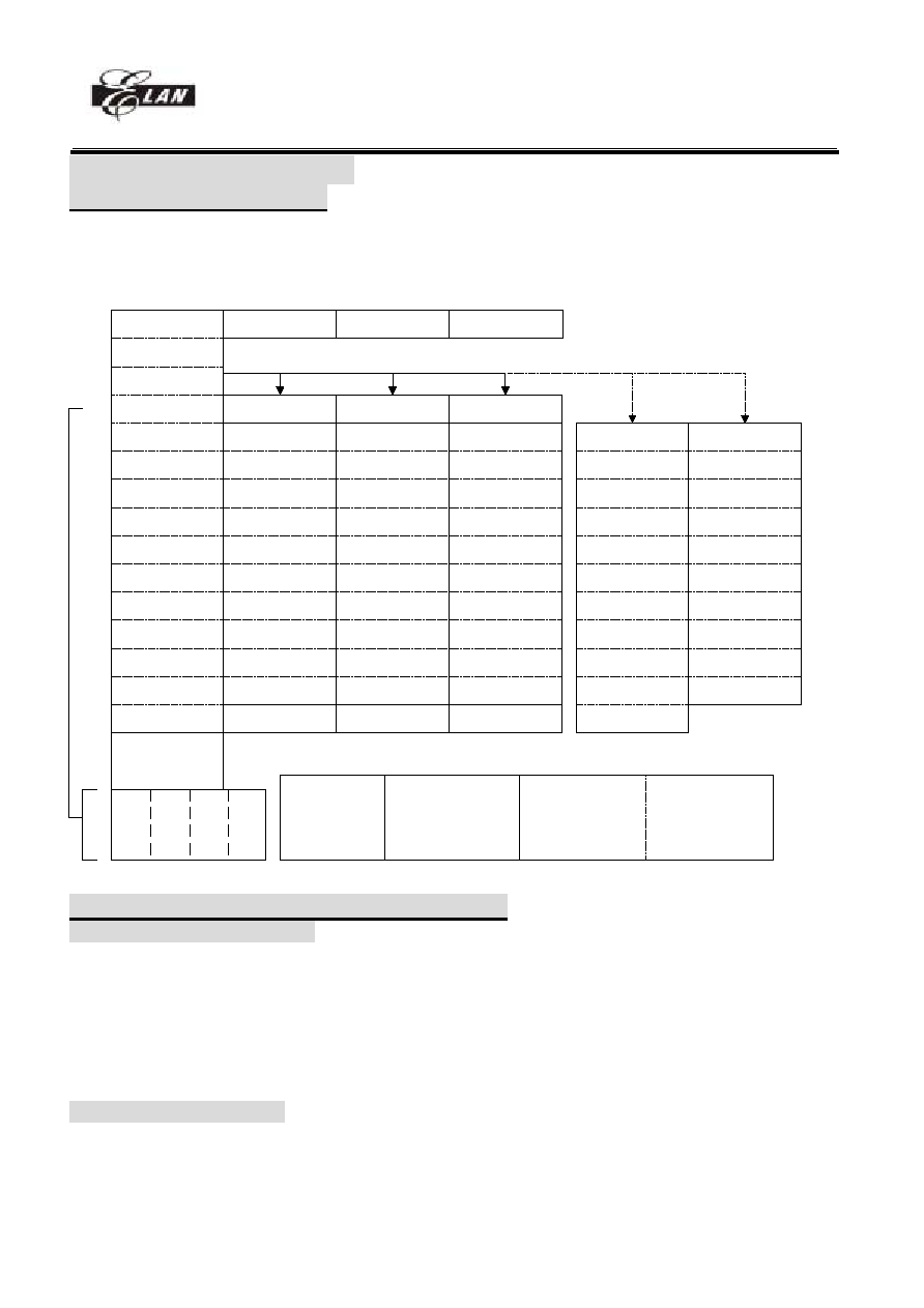
Fig.1_a : EM78P813 die pin assignment

EM78P813
8-bit OTP Micro-controller
__________________________________________________________________________________________________________________________________________________________________
* This specification is subject to change without notice.
6
2004/8/19 (V1.6)
COM9
COM8
COM7
COM6
COM5
COM4
COM3
COM2
COM1
COM0
VC4
VC3
VC2
VC1
VDD
XIN
XOUT
PLLC
TONE
TIP
RING
AVSS
/RESET
P70/INT0
P7
1
/
I
N
T
1
P7
2
/
I
N
T
2
P7
3
/
I
N
T
3
P7
4
/
I
N
T
4
P75/I
N
T5
P
7
6/INT6/KTONE
P7
7
/
I
N
T
7
P60/STGT
P61/EST
P62
P63
P64
P65/CMP1
P66/CMP2
P67/CMP3
PD5/SDO
S
E
G8
2/
P
B
0/
L
D
0
S
E
G8
3/
P
B
1/
L
D
1
S
E
G8
4/
P
B
2/
L
D
2
S
E
G8
5/
P
B
3/
L
D
3
S
E
G8
6/
P
B
4/
L
D
4
SEG
87/PB
5/LD
5
SEG
88/P
B
6/LD
6
S
E
G8
9/
P
B
7/
L
D
7
SE
G
9
0
/
PC0
/
CS2
S
E
G9
1/
P
C
1/
C
S
1
S
E
G9
2/
P
C
2/
W
R
SEG57/RD
SEG58/EXD7
SEG59/EXD6
SEG61/EXD4
SEG60/EXD5
SEG62/EXD3
SEG63/EXD2
SEG64/EXD1
SEG65/EXD0
SEG66/P80
SEG67/P81
SEG68/P82
SEG69/P83
SEG70/P84
SEG71/P85
SEG72/P86
SEG73/P87
SEG74/P90
SEG75/P91
SEG76P92
SEG77/P93
SEG78/P94
SEG79/P95
EXS
E
L
SEG45/EXA9
SEG44/EXA10
SEG43/EXA11
S
E
G4
2/
EX
A1
2
S
E
G4
1/
EX
A1
3
S
E
G4
0/
EX
A1
4
S
E
G3
9/
EX
A1
5
S
E
G3
8/
EX
A1
6
S
E
G3
7/
EX
A1
7
S
E
G3
6/
EX
A1
8
S
E
G3
5/
EX
A1
9
S
E
G3
4/
EX
A2
0
SE
G3
3
SE
G3
2
SE
G3
1
SE
G3
0
SE
G2
9
SE
G2
8
SE
G2
7
SE
G2
6
SE
G2
5
SE
G2
4
SE
G2
3
SE
G2
2
SE
G2
1
SE
G2
0
SE
G1
9
SE
G1
8
SE
G1
7
SE
G1
6
SE
G1
5
SE
G1
4
SE
G1
3
SE
G1
2
SE
G1
1
SE
G
1
0
SE
G
9
SE
G
8
COM13
COM12
COM11
COM10
1
2
3
4
5
6
7
8
9
10
11
12
13
14
15
16
17
18
19
20
21
22
23
24
25
26
27
28
29
30
31
32
33
34
35
36
37
38
39
40
41
42
43
44
45
53 54
55
56
57
58
59
60
61
62
63
64 65 66
67
70
71
72
73 74 75
76
77
78
79
136
137
157
15
8
15
9
16
0
16
1
16
2
16
3
16
4
CHI
P
SEL
CWGS
CWIN
VC5
AVDD
Vout
VREF
C1
C2
COM14
COM15
SE
G
1
SEG0
SE
G
3
SE
G
2
SE
G
5
SE
G
4
SE
G
7
SE
G
6
SEG54/EXA0
SEG53/EXA1
SEG52/EXA2
SEG51/EXA3
SEG50/EXA4
SEG49/EXA5
SEG48/EXA6
SEG47/EXA7
SEG46/EXA8
SEG56/WR
SEG55/CS
SEG80/P96
SE
G
8
1
/
P9
7
SEG
93/PC
3/R
D
SEG
94/P
C
4/A
0
SE
G
9
5
/
PC5
SE
G9
6/P
C
6
SE
G
9
7
/
PC7
CO
M
3
1/S
E
G
9
8
CO
M
3
0
/
S
E
G
9
9
C
O
M29/SEG
100
C
O
M28/SEG
101
C
O
M27/SEG
102
C
O
M26/S
E
G
1
03
COM2
5/S
E
G
1
0
4
COM2
4/S
E
G
1
0
5
C
O
M23
/
SEG
106
C
O
M22
/
SEG
107
C
O
M21
/
SEG
108
C
O
M20
/
SEG
109
C
O
M19
/
SEG
110
C
O
M18
/
SEG
111
CO
M
1
7
CO
M
1
6
PD0
PD1
PD2
PD3
PD4/SCK
LVSS
LVDD
PD6/SDI
PD7/DAOUT
EGIN1
EGIN2
80
81 82 83
84
85
86
87
88
89
90
91 92
93
94
95 96
97
99
98
110
109
108
107
106
105
119
118
117
116
115
114
113
112
111
128
127
126
125
124
123
122
121
120
135
134
133
132
131
130
129
68 69
GND
TE
S
T
46
47
48
49
50
51
52
NC
NC
NC
NC
NC NC NC
NC
NC
NC
NC NC
10
0
10
1
10
2
104
10
3
NC
NC
NC
143
144
142
141
140
139
138
150
151
149
148
147
146
145
156
155
154
153
152
165
16
6
16
7
16
8
16
9
17
0
17
1
17
2
173
17
4
17
5
17
6
17
7
17
8
17
9
18
0
181
18
2
18
3
18
4
18
5
18
6
18
7
18
8
189
19
0
19
1
19
2
19
3
19
4
19
5
19
6
197
19
8
19
9
20
0
20
1
20
2
20
3
20
4
205
20
6
20
7
20
8
NC
NC
NC
NC
NC
NC
NC
NC
NC
NC
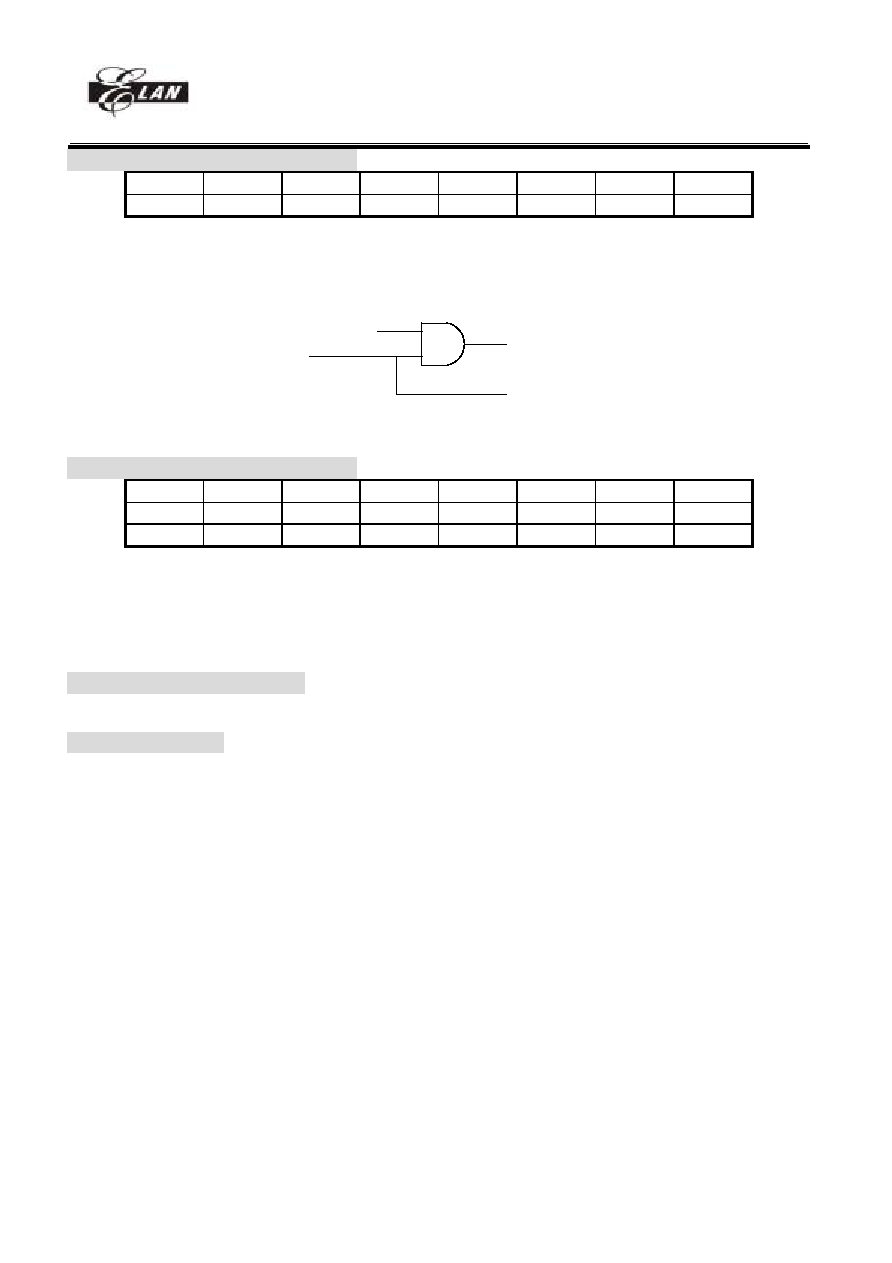
Fig.1_b : EM78P813 208 pin QFP pin assignment
EM78P813
8-bit OTP Micro-controller
__________________________________________________________________________________________________________________________________________________________________
* This specification is subject to change without notice.
7
2004/8/19 (V1.6)
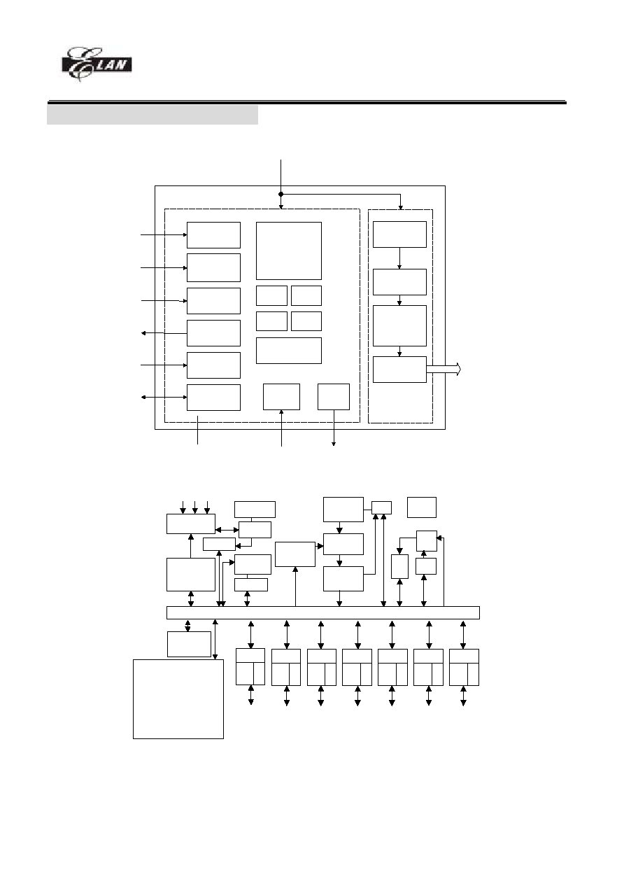
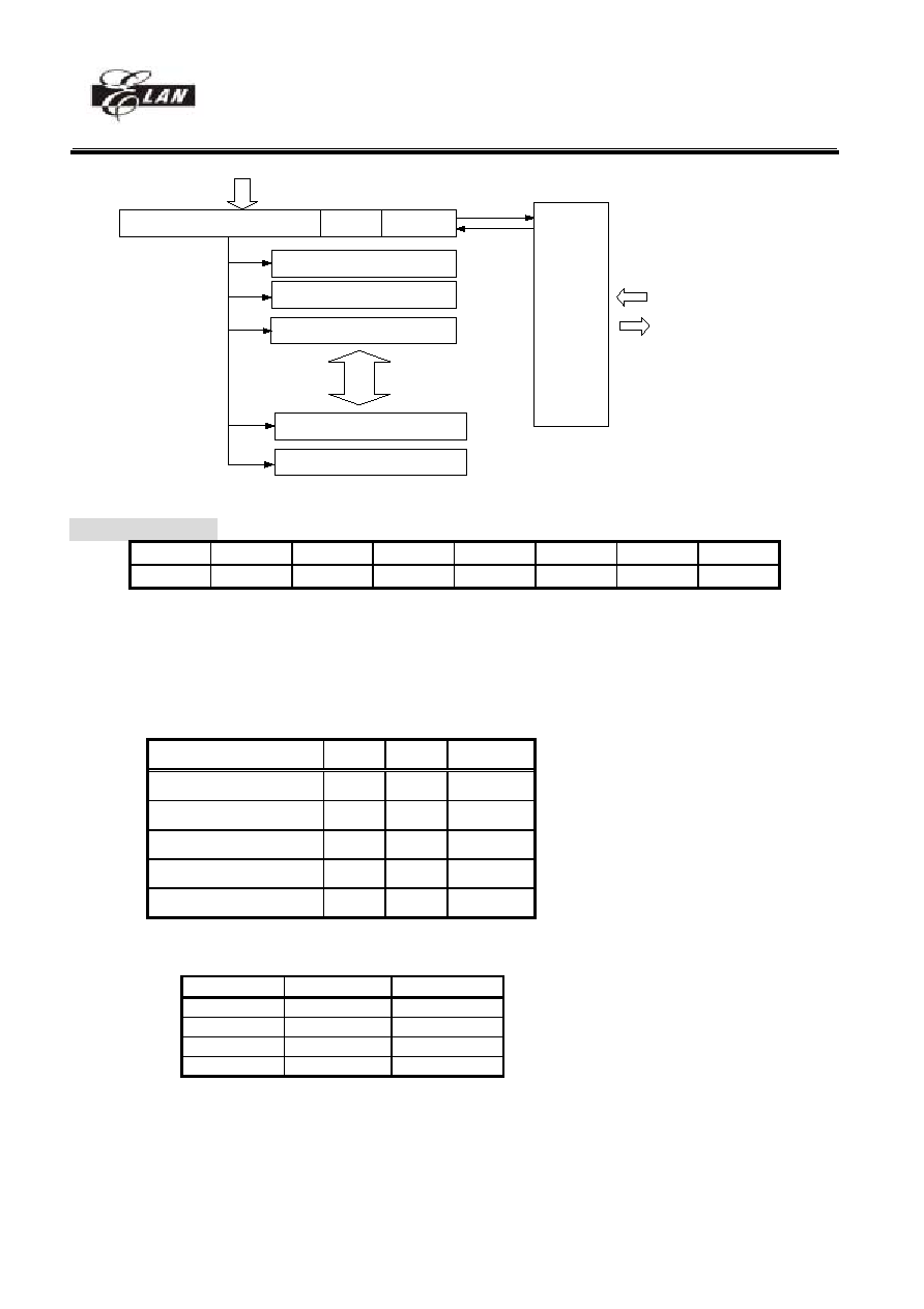
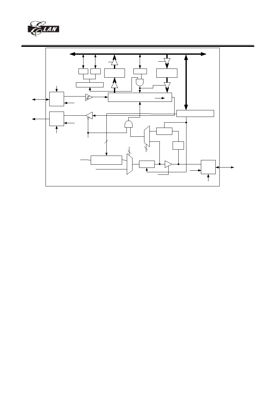
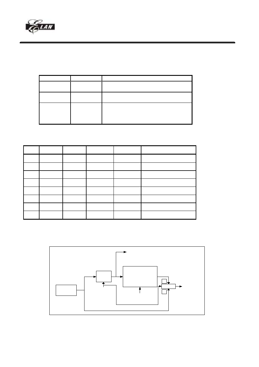
V. Functional Block Diagram
Program
ROM
DATA
ROM
DATA
RAM
MCU
PLL
FSK
Decoder
Dual Tone
Generator
DTMF
Receiver
Energy
Detector
Comparator
Serial IO
(SPI/UART)
LCD
RAM
Current
DA
CW
Decoder
VDD
AVDD
Voltage
Regulator
X 2
Charge Pump
V1~V5
Generator &
driving ability
control
LCD
driver
COM&SEG
2.7 V
DTMF
signal
FSK
signal
CAS
TONE
Analog
input
Data
FSK DTMF CAS
signal
DAOUT
VSS
AVSS
Fig.2 Block diagram1
Xin Xout PLLC
Oscillator
timing control
Control sleep
and wake-up
on I/O port
R1(TCC)
WDT timer
prescalar
GENERAL
RAM
R4
Interruption
control
ROM
Instruction
register
Instruction
decoder
R2
STACK
ALU
ACC
R3
R5
DATA & CONTROL BUS
DATA RAM
DATA ROM
PORT6
IOC6 R6
P60~P67
PORT7
IOC7 R7
P70~P77
FSK DECODER
DTMF receiver
DUAL TONE GENERATOR
KEY TONE
SERIAL I/O
COMPARATOR
FSK DECODER
DTMF receiver
DUAL TONE GENERATOR
KEY TONE
SERIAL I/O
COMPARATOR
CURRENT DA
PORT8
IOC8 R8
P80~P87
PORT9
IOC9 R9
P90~P97
PORTB
IOCB RB
PB0~PB7
PORTC
IOCC RC
PC0~PC7
Call waiting decoder
Energy Detector
PORTD
IOCD RD
PD0~PD2
LCD RAM
Fig.3 Block diagram2
EM78P813
8-bit OTP Micro-controller
__________________________________________________________________________________________________________________________________________________________________
* This specification is subject to change without notice.
8
2004/8/19 (V1.6)
VI. Pin Descriptions
I. POWER pin
Pin I/O
Description
VDD POWER
Digital
Power
AVDD POWER
Analog
Power
LVDD
POWER
Charge pump used power
GND POWER
Digital
Ground
AVSS
POWER Analog Ground
LVSS
POWER
Charge pump used power
II. CLOCK pin
Pin I/O
Description
XIN
I
Input pin for 32.768 kHz oscillator
XOUT
O
Output pin for 32.768 kHz oscillator
PLLC
I
Phase loop lock capacitor, connect a capacitor 0.01u to 0.047u
with GND
III.1. Embedded LCD pin
Pin I/O
Description
COM0..COM15
O
Common driver pins of LCD drivers
COM16..COM23
O
COM16..COM23 are shared with SEG111..SEG106
COM24..COM31
O
COM24..COM31 are shared with SEG105..SEG98
SEG0..SEG65
O
Segment driver pins of LCD drivers
SEG66..SEG73
O
Segment driver pins of LCD drivers share with PORT8
SEG74..SEG81
O
Segment driver pins of LCD drivers share with PORT9
SEG82..SEG89
O
Segment driver pins of LCD drivers share with PORTB
SEG90..SEG97
O
Segment driver pins of LCD drivers share with PORTC
C1,C2
-
Charge Pump capacitor. C1 connect 1uF Cap To C2.
Vout
-
Charge pump output voltage ,connect 1uF Cap to GND
VREF
-
2.7V, need to be connected 0.1uF capacitor to GND
VC1..VC5
I
Reference voltage input. Each one connect a capacitor (0.1u)
with GND.
III.2. External LCD device control pin
Pin I/O
Description
LCDD0..LCDD7
I/O
External LCD driver data bus. Shared with PORTB0..PORTB7.
/WR
O
Write enable output (active low signal). Shared with PORTC2.
/RD
O
Read enable output (active low signal). Shared with PORTC3.
A0 O
Used as register selection. When A0 equal to 1, data bus transmit
LCD DATA. When A0 equal to 0,data bus transmit LCD
Address. The pin shared with PORTC4.
/CS1../CS2 O
Chip
Selection
signal
output. Shared with PORTC1..PORTC0
IV. FSK,CW
Pin I/O
Description
TIP
I
Should be connected with TIP side of twisted pair lines for FSK.
RING
I
Should be connected with RING side of twisted pair lines for
FSK.
CWGS
O
Gain adjustment of single-ended input OP Amp
CWIN
I
Single-ended input OP Amp for call waiting decoder
EGIN1,EGIN2 I
DED
input
V. DTMF receiver
Pin I/O
Description
EST O
Early steering output. Presents a logic high immediately when
EM78P813
8-bit OTP Micro-controller
__________________________________________________________________________________________________________________________________________________________________
* This specification is subject to change without notice.
9
2004/8/19 (V1.6)
the digital algorithm detects a recognizable tone-pair (signal
condition). Any momentary loss of signal condition will cause
EST to return to a logic low. This pin shared with PORT61.
STGT
I/O
Steering input/guard time output (bi-directional). A voltage
greater than Vtst detected at ST causes the device to register the
detected tone-pair and update the output latch.
A voltage less than Vtst frees the device to accept a new
tone-pair. The GT output acts to reset the external steering
time-constant; its state is a function of EST and the voltage on
ST . This pin shared with PORT60.
VI. Serial IO, Comparator , Current DA , Tone
Pin I/O
Description
SCK
I/O
Master: output pin , Slave: input pin. This pin shared with
PORTD4
SDO
O
Output pin for serial data transferring. This pin shared with
PORTD5.
SDI
I
Input pin for receiving data. This pin shared with PORTD6.
CMP1
I
Comparator input pins. Shared with PORT65.
CMP2
I
Comparator input pins. Shared with PORT66
CMP3
I
Comparator input pins. Shared with PORT67.
DAOUT
O
Current DA output pin. It can be a control signal for sound
generating. Shared with PORTD7.
KTONE
O
Key tone output. Shared with PORT76.
TONE
O
Dual tone output pin
VII. IO
Pin I/O
Description
P60 ~P67
I/O
PORT 6 can be INPUT or OUTPUT port each bit.
Internal pull high.
P70 ~ P77
I/O
PORT 7 can be INPUT or OUTPUT port each bit.
Internal Pull high function.
Auto key scan function.
Interrupt function.
Shared with Key tone output
P80 ~ P87
I/O
PORT 8 can be INPUT or OUTPUT port each bit.
Shared with LCD Segment signal.
P90 ~ P97
I/O
PORT 9 can be INPUT or OUTPUT port each bit.
Shared with LCD Segment signal.
PB0 ~ PB7
I/O
PORT B can be INPUT or OUTPUT port each bit.
Shared with LCD Segment signal.
PC0 ~ PC7
I/O
PORT C can be INPUT or OUTPUT port each bit.
Shared with LCD Segment signal.
PD0 ~ PD7
I/O
PORT D can be INPUT or OUTPUT port each bit.
Shared with SPI pin
Share with CMP input pin.
P70 ~ P76
I
Interrupt sources. Any pin from PORT70 to PORT76 has a
falling edge signal, it will generate a corresponding
interruption..
P77
I
Interrupt source. Once PORT77 has a falling edge or rising edge
signal (controlled by CONT register), it will generate a
interruption.
/RESET I
Low
reset
EM78P813
8-bit OTP Micro-controller
__________________________________________________________________________________________________________________________________________________________________
* This specification is subject to change without notice.
10
2004/8/19 (V1.6)
VIII Expand Program/Data ROM interface
Pin I/O
Description
EXD0 ~ EXD7
I/O
Expand Program/Data memory Data Bus
RD
O
Expand Program/Data memory Read request output
WR
O
Expand Program/Data memory Write request output
CS
O
Expand Program/Data memory CS request output
EXA-1~EXA19 O
Expand
Program/Data
memory
Address
Bus
EXSEL I
0/1
Internal 64K Program ROM select used/unused
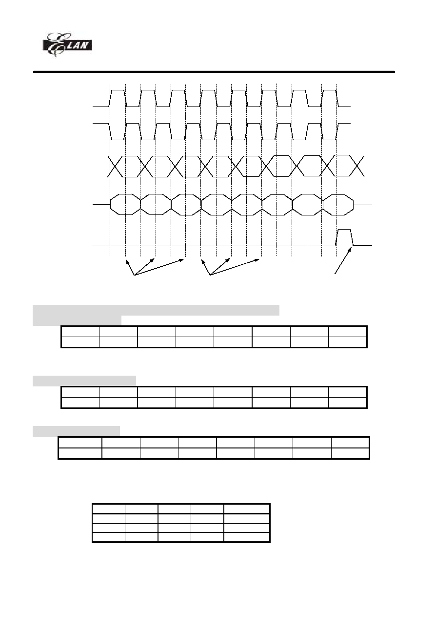
CHIPSEL Pin : EM78813 or EM78815 function select . In EM78813 mode , Key strobe pin are share with SEG50 ~ SEG
65. If select to EM78815 mode , Key strobe pin are share with I/O Port8 and Port9. SEG34 ~SEG65 pin will switch
to expand flash memory interface.
Connect to ground EM78813 mode
Connect
to
VDD
EM78815 mode
EM78813 mode
COM2
SEG
V1
V2
V4
V5
GND
30us
V1
V2
V4
V5
GND
V1
V2
V4
V5
GND
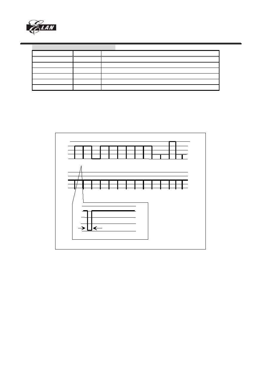
Fig.4(a) : EM78813 mode Key scan signal(share with SEG pin)
EM78815 mode (must set RE page2 bit2 ~ bit4 = 1)
30us
Key scan pin(P8,P9)
VDD
GND
Fig.4(b) : EM78815 mode Key scan signal(share with IO pin)
EXSEL pin : 0/1 On-Chip program ROM used/unused switch
(EM78815 mode only)
.
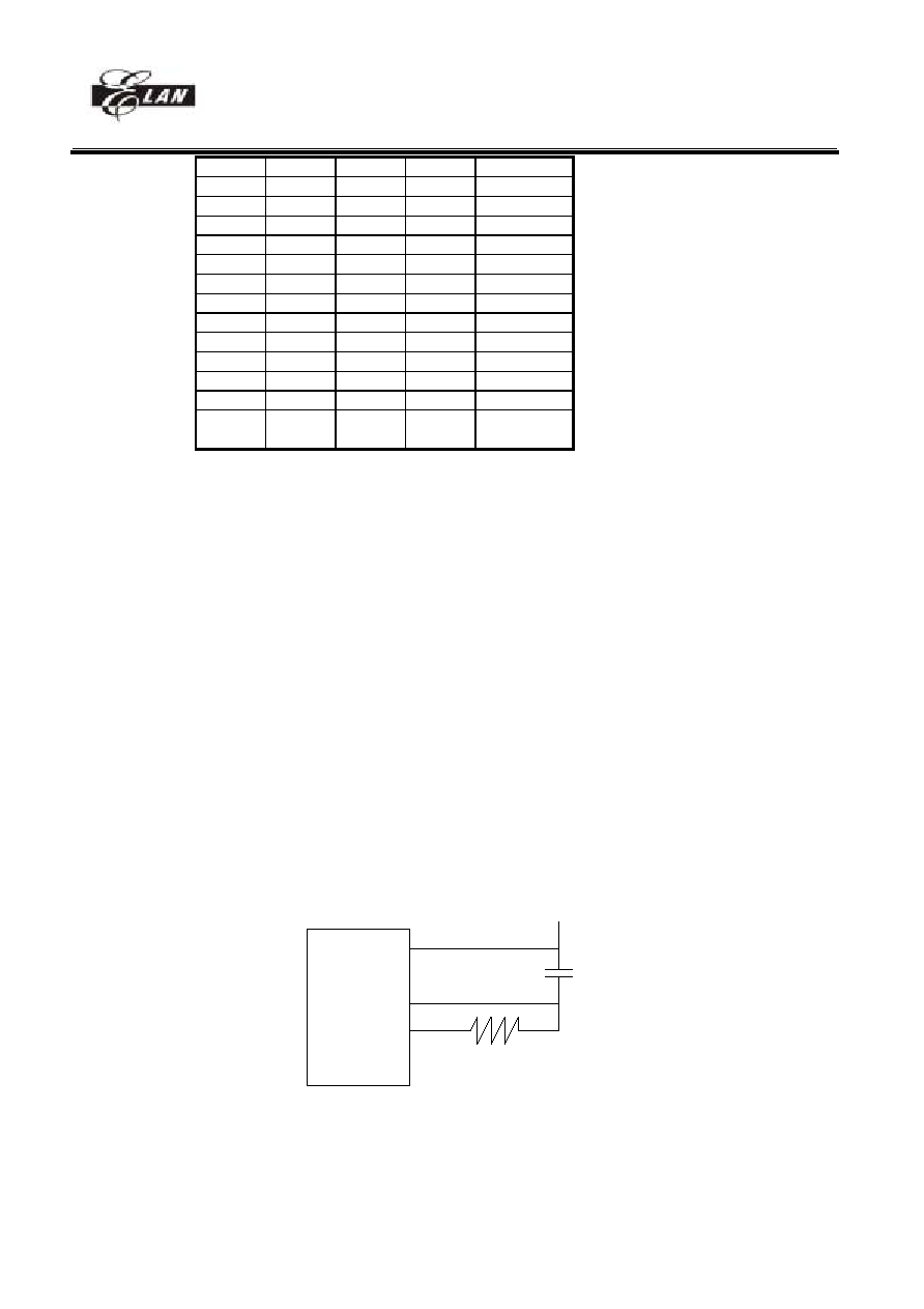
EM78P813 support MAX 128K Program . User can port program to both 64K EM78P813 on_chip ROM and
64K expand ROM . User also can ignore 64K EM78P813 on_chip ROM and porting all programs to a external
128K ROM. Using this function, user can upgrade program or download new function easily.
EM78P813 provide Data ROM expand function. When user access data which address is over 256K, external
ROM will be load. User must set expand start address of Data ROM to RF PAGE1, PAGE2 and IOCB PAGE1. A
diagram of expand function is as below.
64K Program ROM
(PAGE0 ~ PAGE 63)
256K byte
Data ROM
EM78P813
(EXSEL pin go low)
MAX 2M Byte Expand ROM
(FLASH ROM)
64K word Program ROM
(PAGE64~PAGE127)
ExpandData ROM
Expand Data ROM start address
0
X
X
X
X
X
X
X
X
X
X
X
X
X
X
X
X
X
0
0
RF PAGE1
RF PAGE2
0
ROM
Address
0
ROM
Address
9
ROM
Address
17
b0
b0
b7
b7
IOCB
B7
Fig5(a) : EXSEL = 0,both internal and external program are used.
EM78P813
8-bit OTP Micro-controller
__________________________________________________________________________________________________________________________________________________________________
* This specification is subject to change without notice.
12
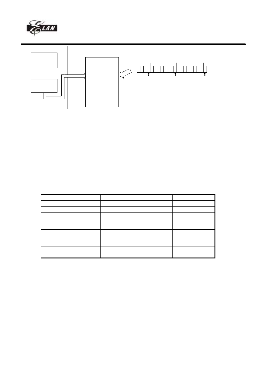
2004/8/19 (V1.6)
64K Program ROM
Unused
256K byte
Data ROM
EM78P813
(EXSEL pin pull high)
MAX 2M Byte Expand ROM
(FLASH ROM)
128K word Program ROM
(PAGE0~PAGE127)
ExpandData ROM
Expand Data ROM start address
0
X
X
X
X
X
X
X
X
X
X
X
X
X
X
X
X
X
0
0
RF PAGE1
RF PAGE2
0
ROM
Address
0
ROM
Address
9
ROM
Address
17
b0
b0
b7
b7
IOCB
B7
Fig5(b) : EXSEL = 1, only external program are used.
How to set start address for expanding Data ROM?
EM78815 support maximum 2M Byte expanding data memory, but user must fix the start address of external
program at 0x00000 and set start address of expanding Data ROM by user. By this way, MCU will get data from external
memory if the data ROM is over 256K.
The width of an instruction is 13 bit and the data bus for external memory is 8bit, so an instruction will captured two
address size and the LSB address of start address at external ROM will be 0. Besides, EM78815 only support MAX 128K
program, so the start address of Data ROM will smaller than 256K-2 andA20, A19 and A18 will be 0 also. User only has to
according to write Data ROM address A17~A1 to IOCB PAGE2 bi7,RF PAGE3 and RF PAGE2.
EM78P813 writer pin
OTP writer PIN NAME
MASK ROM PIN NAME
P.S.
1.VDD VDD,AVDD
2.VPP /RESET
3.DINCK P77
4.ACLK P76
5.PGM P75
6.OE P74
7.DATA P73
8.GND VSS,AVSS,TEST
9.ROMSEL
P72
High : Data ROM
Low : Program ROM
EM78P813
8-bit OTP Micro-controller
__________________________________________________________________________________________________________________________________________________________________
* This specification is subject to change without notice.
13
2004/8/19 (V1.6)
VII. Function Descriptions
VII.1 Operational Register
05
06
07
08
09
0A
0B
0C
0D
0E
0F
04
03
02
01
R1(TCC Buffer)
R2(PC)
R3(STATUS)
R4(RSR,bank select)
R5(Program page)
R6(Port6 IO data)
R5(Counter setting)
R5(CNT1 low 8 bit data) R5( CurrentDA control)
R6(DROM data buffer)
R6(CNT1 high 8 bit data) R6(CurrentDA control)
R7(Port7 IO data)
R8(Port8 IO data)
R9(Port9 IO data)
RB(PortB IO data)
RC(PortC IO data)
RD(PortD IO data)
R7(DROM address)
R8(DROM address)
R7(CNT2 data)
R7(SPI control)
R8(DTMF receiver)
R8(SPI data buffer)
R9(DROM address ,
LCD address MSB )
R9(CMP IO control)
R9(Key tone control)
RA(Power saving , FSK) RA(LCD address)
RA(Comparator control) RA(Tont1 control)
RB(LCD data buffer)
RB(Key strobe control)
RB(Tone2 control)
RC(DRAM1 data buffer)
RD(DRAM1 address)
RC(Key strobe control)
RD(LCD control)
RE(Interrupt flag1)
RF(Interrupt flag2)
RE(DRAM1 address ,
DED output)
RE(LCD control ,
Key scan , CAS)
IOC5(Address auto
inc/dec control)
IOC5(DRAM2 data buffer)
IOC6(Port6 I/O control)
IOC6(DRAM2 address)
IOC7(Port7 I/O control)
IOC8(Port8 I/O control)
IOC9(Port9 I/O control)
IOCB(PortB I/O control)
IOCC(PortC I/O control)
IOCD(PortD I/O control)
IOC7(DRAM2 address)
IOC8(IO/SEG switch)
IOC9(PB I/O/SEG switch)
IOCA(PC I/O/SEG switch)
IOCA(STACK point)
IOCB(External LCD driver
control interface)
IOCC(P6 pull high control)
IOCD(P7 pull high control)
IOCE(Interrupt mask1)
IOCE(DED control)
IOCE(Interrupt mask2)
16 Byte Commom register
10
:
1F
Bank0
Bank1
Bank2 Bank3
32x8
32x8
32x8
32x8
Commom register
20
:
3F
R3(6,7)
R3(5)
R4
P1(7,8)
P3(7)
Address
REGISTER
PAGE0
REGISTER
PAGE1
REGISTER
PAGE2
REGISTER
PAGE3
Control
REGISTER
PAGE0
Control
REGISTER
PAGE1
LCD RAM
RA PAGE1 : address
RB PAGE1 : data
DATA ROM
R7 PAGE1 : address(L)
R8 PAGE1 : address(M)
R9 PAGE1 : address(H)
R6 PAGE1 : data
DATA RAM(index1)
RD PAGE1 : address(L)
RE PAGE1 : address(H)
RC PAGE1 : data
DATA RAM(index2)
IOC6 PAGE1 : address(L)
IOC7 PAGE1 : address(H)
IOC5 PAGE1 : data
R4(Unused)
R4(Undefined)
R4(Undefined)
RC(Undefined)
RD(Undefined)
RE(Undefined)
R1(UART receiver buffer)
RF(Undefined)
R1(Real Interrupt flag1) R1(Real Interrupt flag2)
RF(External Data ROM
Start address LOW)
RF(External Data ROM
Start address HIGH)
Fig.6: control register configuration
VII.2 Operational Register Detail Description
R0 Indirect Addressing Register
R0 is not a physically implemented register. It is useful as indirect addressing pointer. Any instruction using R0 as
register actually accesses data pointed by the RAM Select Register (R4).
Example:
Mov A , @0x20 ;store a address at R4 for indirect addressing
Mov 0x04 , A
Mov A , @0xAA ;write data 0xAA to R20 at bank0 through R0
Mov 0x00 , A
R1 PAGE0 TCC data buffer
TCC data buffer. Increased by 16.38KHz or by the instruction cycle clock (controlled by CONT register).Written and
read by the program as any other register.
EM78P813
8-bit OTP Micro-controller
__________________________________________________________________________________________________________________________________________________________________
* This specification is subject to change without notice.
14
2004/8/19 (V1.6)
R1 PAGE1 Interrupt Flag1 real value
7 6 5 4 3 2 1 0
INTR7 INTR6
INTR5 INTR4
INTR3
INTR2
INTR1 INTR0
Bit 0~Bit 7(INTR0~INTR7) : Interrupt flag1 real value. The relation of R1 Page1, RE PAGE0 and IOCE PAGE0 is
shown in fig. When user disable interrupt mask, whether interrupt occur or not , interrupt flag(RE PAGE0) will
appear "0". Opposite of RE PAGE0, R1 PAGE1 will show real interrupt occur status regardless this interrupt
mask enable or disable. User can clear corresponding external interrupt flag by RE PAGE0 or R1 PAGE1.
Interrupt
Mask
IOCE,IOCF
Interrupt
Flag(RE,RF)
Interrupt
occur
Real Interrupt
Flag(R0 P1,P2)
Fig7 : Relation with interrupt mask ,flag and real flag
R1 PAGE2 Interrupt Flag2 real value
7 6 5 4 3 2 1 0
RBF/STD FSK/CW
X
X
DED
CNT2
CNT1
TCC
R/W-0 R/W-0 R/W-0 R/W-0 R/W-0 R/W-0 R/W-0 R/W-0
Bit 0~Bit 3, Bit 6~Bit 7(Internal interrupt flag real value) : Interrupt flag1 real value. The relation of R1 Page2, RF
PAGE0 and IOCF PAGE0 is shown in fig7. When user disable interrupt mask, whether interrupt occur or not ,
interrupt flag(RF PAGE0) will appear "0". Opposite of RF PAGE0, R1 PAGE1 will show real interrupt occur
status regardless this interrupt mask enable or disable. User can clear corresponding interrupt flag in RF
PAGE0 or R1 PAGE2.
Bit 4~ Bit 5 : Undefined register, these two bits are not allowed to use.
R1 PAGE3 Undefined Register
R1 page3 is undefined register, this is not allowed to use.
R2 Program Counter
External 128K
� 13 PROGRAM ROM addresses to the relative programming instruction codes. The structure is
depicted in Fig.8
"JMP" instruction allows the direct loading of the low 10 program counter bits.
"CALL" instruction loads the low 10 bits of the PC, PC+1, and then push into the stack.
"RET'' ("RETL k", "RETI") instruction loads the program counter with the contents at the top of stack.
"MOV R2,A" allows the loading of an address from the A register to the PC, and the ninth and tenth bits are cleared to
"0''.
"ADD R2,A" allows a relative address be added to the current PC, and contents of the ninth and tenth bits are cleared
to "0''.
"TBL" allows a relative address be added to the current PC, and contents of the ninth and tenth bits don't change. The
most significant bit (A10~A14) will be loaded with the content of bit PS0~PS3 in the status register (R5) upon the
execution of a "JMP'', "CALL'', "ADD R2,A'', or "MOV R2,A'' instruction.
If a interrupt trigger, PROGRAM ROM will jump to address 8 at page0. The CPU will store ACC,R3 status and R5
PAGE automatically, it will restore after instruction RETI.
EM78P813
8-bit OTP Micro-controller
__________________________________________________________________________________________________________________________________________________________________
* This specification is subject to change without notice.
15
2004/8/19 (V1.6)
A16 A15 A14 A13 A12 A11 A10 A9 A8 A7~A0
0000000 PAGE0 00000~003FF
0000001 PAGE1 00400~007FF
1111110 PAGE126 1F800~1FBFF
1111111 PAGE127 1FC00~1FFFF
0000010 PAGE2 00800~00BFF
STACK1
STACK2
STACK5
STACK4
STACK3
STACK6
STACK8
STACK7
:
:
STACK30
STACK31
STACK32
CALL
and
INTERRUPT
RET
RETL
RETI
ACC,R3,R5(PAGE)
R5(PAGE)
store
restore
Fig.8 : Program counter organization
R3 Status Register
7 6 5 4 3 2 1 0
RS1
RS0
IOCS
T P Z DC C
Bit 0 (C) : Carry
Bit 1 (DC) : Auxiliary carry flag
Bit 2 (Z) : Zero flag
Bit 3 (P) : Power down bit.
Set to 1 during power on or by a "WDTC" command and reset to 0 by a "SLEP" command.
Bit 4 (T) : Time-out bit.
Set to 1 by the "SLEP" and "WDTC" command, or during power up and reset to 0 by WDT timeout.
EVENT T
P
REMARK
WDT wake up from sleep mode
0
0
WDT time out (not sleep mode)
0
1
/RESET wake up from sleep
1
0
Power up
1
1
Low pulse on /RESET
x
X
x : don't care
Bit 5 (IOCS) : IOC register select bit. Change IOC5 ~ IOCE to another PAGE
Bit 6~Bir 7 (RS0 ~ RS1) : R register select bits. Change R5 ~ RE to another PAGE.
RS1 RS0
R
PAGE
0 0
PAGE
0
0 1
PAGE
1
1 0
PAGE
2
1 1
PAGE
3
EM78P813
8-bit OTP Micro-controller
__________________________________________________________________________________________________________________________________________________________________
* This specification is subject to change without notice.
16
2004/8/19 (V1.6)
R4 RAM select for common Registers R20~R3F , UART control
PAGE0
7 6 5 4 3 2 1 0
RBS1 RBS0 RSR5 RSR4 RSR3 RSR2 RSR1 RSR0
Bit 0 ~ Bit 5 (RSR0 ~ RSR5) : Indirect addressing for common registers R20 ~ R3F
RSR bits are used to select up to 32 registers (R20 to R3F) in the indirect addressing mode.
Bit 6 ~ Bit 7 (RB0 ~ RB1) : Bank selection bits for common registers R20 ~ R3F
These selection bits are used to determine which bank is activated among the 4 banks (RBS2 is in R4 PAGE3 Bit7)
for 32 register (R20 to R3F)..
R4 PAGE1 Undefined Register
R4 page1 is undefined register, this is not allowed to use.
PAGE2 Undefined Register
7 6 5 4 3 2 1 0
X X X X X X 0 0
R/W-0
R/W-0
R/W-0
R/W-0
R/W-0
R/W-0
R/W-0
R/W-0
Bit 0 ~ Bit 1 : Undefined registers, please clear these two bits to 0.
Bit 2 ~ Bit 7 : Undefined registers, these bits are not allowed to use.
R4 PAGE3 Undefined Register
R4 page3 is undefined register, this is not allowed to use.
R5 Program page selection , CNT CLK & scale setting , CNT1 data(L)
PAGE0 Program page
7 6 5 4 3 2 1 0
X PS6 PS5 PS4 PS3 PS2 PS1 PS0
X R/W-0 R/W-0 R/W-0 R/W-0 R/W-0 R/W-0 R/W-0
Bit 0 ~ Bit 6 (PS0 ~ PS6) : Program page selection bits
PS6 PS5 PS4 PS3 PS2 PS1 PS0 Program
memory
page
(Address)
0 0 0 0 0 0 0
Page
0
0 0 0 0 0 0 1
Page
1
0 0 0 0 0 1 0
Page
2
0 0 0 0 0 1 1
Page
3
: : : : :
:
: : : : :
:
1 1 1 1 1 1 0
Page
126
1 1 1 1 1 1 1
Page
127
User can use PAGE instruction to change page to maintain program page by user.
Bit 7 : Unused.
PAGE1 Counter1 Counter2 CLK and scale setting
7 6 5 4 3 2 1 0
CNT2S C2P2 C2P1 C2P0 CNT1S
C1P2 C1P1 C1P0
Bit 0~Bit 2(C1P0~C1P2) : Counter1 scaling
EM78P813
8-bit OTP Micro-controller
__________________________________________________________________________________________________________________________________________________________________
* This specification is subject to change without notice.
17
2004/8/19 (V1.6)
C1P2 C1P1 C1P0
COUNTER1
0 0 0 1:2
0 0 1 1:4
0 1 0 1:8
0 1 1 1:16
1 0 0 1:32
1 0 1 1:64
1 1 0 1:128
1 1 1 1:256
Bit 3 (CNT1S) : Counter1 clock source
0/1 16.384kHz/instruction clock
Bit 4~Bit 6(C2P0~C2P2) : Counter2 scaling. Prescaler is as different as Bit 0~Bit 2.
C2P2 C2P1 C2P0
COUNTER2
0 0 0 1:2
0 0 1 1:4
0 1 0 1:8
0 1 1 1:16
1 0 0 1:32
1 0 1 1:64
1 1 0 1:128
1 1 1 1:256
Bit 7 (CNT2S) : Counter2 clock source
0/1 16.384kHz/instruction clock
PAGE2 Counter 1 Low 8bit Data buffer
7 6 5 4 3 2 1 0
CN17 CN16 CN15 CN14 CN13 CN12 CN11 CN10
Bit 0~Bit 7(CN10~CN17) : Counter1's data buffer
User can switch Counter1 between 8 bits or 16 bits counter by setting Control register bit 4. When CNT1BS set
to 0, counter1 is a 8 bits up-counter with 8-bit prescaler that user can use R5 page2 to preset and read the counter.
( write = preset). Else counter1 will be a 16 bits up-counter with 8-bit prescaler and user can read or write the counter
through R5 page2 and R6 page2. After a interruption, it will reload the preset value.
Example: write: MOV 0x05,A ; write the data at accumulator to counter1 (preset)
Example: read: MOV A,0x05 ; read R5 data and write to accumulator
Example: write: MOV 0x06,A ; write the data(high 8 bits) at accumulator to counter1
Example: read: MOV A,0x06 ; read R6 data(high 8 bits) and write to accumulator
PAGE3 Current DA Control
7 6 5 4 3 2 1 0
X X X X
CDAS
CDAL2
CDAL1
CDAL0
R-X R-X R-X R-X R/W-0
R/W-0
R/W-0
R/W-0
Bit 0 ~ Bit 2 (DAL0 ~ DAL2) : change output level of current DA
CDAL2 CDAL1
CDAL0 Output
level
0
0
0
L0 (ratio = 1/8)
0
0
1
L1 (ratio = 2/8)
0
1
0
L2 (ratio = 3/8)
0
1
1
L3 (ratio = 4/8)
1
0
0
L4 (ratio = 5/8)
1
0
1
L5 (ratio = 6/8)
1
1
0
L6 (ratio = 7/8)
1 1 1
L7
(ratio
=1)
EM78P813
8-bit OTP Micro-controller
__________________________________________________________________________________________________________________________________________________________________
* This specification is subject to change without notice.
18
2004/8/19 (V1.6)
Bit 3 (CDAS) : Current DA switch
0 normal PORTD7
1 Current DA output
Bit 4 ~ Bit 7 : These 4 bits are undefined, they are not allowed to use.
R6 Port 6 I/O Data , Data ROM data buffer,CNT1 Data(H),DA control
PAGE0 Port 6 I/O Data
7 6 5 4 3 2 1 0
P67 P66 P65 P64 P63 P62 P61 P60
R/W-X R/W-X
R/W-X R/W-X
R/W-X
R/W-X
R/W-X R/W-X
Bit 0 ~ Bit 7 (P60 ~ P67) : 8-bit PORT6 (0~7) I/O data register
User can use IOC register to define input or output each bit..
PAGE1 Data ROM Data buffer
7 6 5 4 3 2 1 0
DRD7 DRD6 DRD5 DRD4 DRD3 DRD2 DRD1 DRD0
R/W-X R/W-X
R/W-X R/W-X
R/W-X
R/W-X
R/W-X R/W-X
Bit 0 ~ Bit 7 (DRD0 ~ DRD7) : Data ROM data buffer for ROM reading.
Example.
MOV A,@1
MOV R7_PAGE1,A
MOV A,@0
MOV R8_PAGE1,A
MOV A,@0
MOV R9_PAGE1,A
MOV A,R6_PAGE1
;read the data at Data ROM which address is "00001".
PAGE2 Counter1 high 8bit Data buffer
7 6 5 4 3 2 1 0
CN1F CN1E CN1D CN1C CN1B CN1A CN19 CN18
Bit 0~Bit 7(CN18~CN1F) : Counter1's high 8 bits data buffer. Please refer to IOC9 page2 counter1 low 8 bit data buffer
for detail.
PAGE3 DA Control
7 6 5 4 3 2 1 0
DA9 DA8 DA7 DA6 DA5 DA4 DA3 DA2
R/W-0 R/W-0 R/W-0 R/W-0 R/W-0 R/W-0 R/W-0 R/W-0
Bit 0 ~ Bit 7 (DA2 ~ DA9) : Current DA most significant 8 bits of Current DA output buffer
Combine these 8 bits and R9 page3 bit4~bit5 2 bits as complete 10 bits Current DA output data. Control
register bit3 is Current DA power control .
EM78P813
8-bit OTP Micro-controller
__________________________________________________________________________________________________________________________________________________________________
* This specification is subject to change without notice.
19
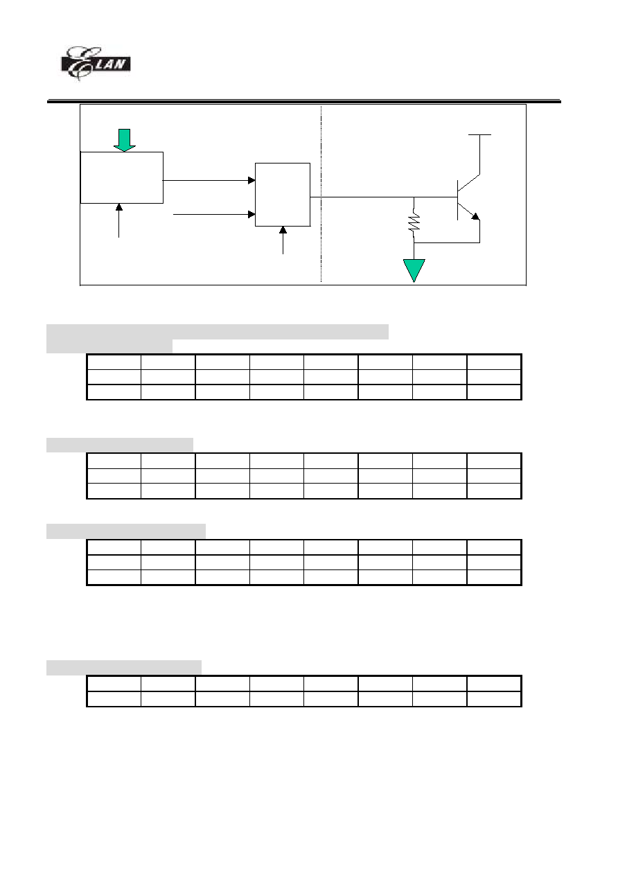
2004/8/19 (V1.6)
MUX
PORTD7
DAOUT
DAS
current DA
circuit
DAEN
DA9..DA0
PORTD7
VDD
Fig.12 Current DA structure
R7 Port 7 I/O Data , Data ROM address , CNT2 Data , SPI control
PAGE0 Port 7 I/O Data
7 6 5 4 3 2 1 0
P77 P76 P75 P74 P73 P72 P71 P70
R/W-X R/W-X
R/W-X R/W-X
R/W-X
R/W-X
R/W-X R/W-X
Bit 0 ~ Bit 7 (P70 ~ P77) : 8-bit PORT7(0~7) I/O data register
User can use IOC register to define input or output each bit.
PAGE1 Data ROM address
7 6 5 4 3 2 1 0
DRA7 DRA6 DRA5 DRA4 DRA3 DRA2 DRA1 DRA0
R/W-X R/W-X
R/W-X R/W-X
R/W-X
R/W-X
R/W-X R/W-X
Bit 0 ~ Bit 7 (DRA0 ~ DRA7) : Data ROM address ( 0~7 ) for ROM reading
PAGE2 Counter2 Data buffer
7 6 5 4 3 2 1 0
CN27 CN26 CN25 CN24 CN23 CN22 CN21 CN20
R/W-0 R/W-0 R/W-0 R/W-0 R/W-0 R/W-0 R/W-0 R/W-0
Bit 0~Bit 7(CN20~CN27) : Counter2's data buffer
User can read and write this buffer. Counter2 is a eight bit up-counter with 8-bit prescaler that user can use R7
page2 to preset and read the counter. ( write = preset) After a interruption, it will reload the preset value.
Example: write: MOV 0x07 , A ; write the data at accumulator to counter1 (preset)
Example: read: MOV A , 0x07 ; read R7 data and write to accumulator
PAGE3 SPI Control Register
7 6 5 4 3 2 1 0
RBF SPIE SRO SE SCES SBR2 SBR1 SBR0
Fig.7 shows how SPI to communicate with other device by SPI module. If SPI is a master controller, it sends clock
through the SCK pin. An 8-bit data is transmitted and received at the same time. If SPI, however, is defined as a slave,
its SCK pin could be programmed as an input pin. Data will continue to be shifted on a basis of both the clock rate and
the selected edge.
EM78P813
8-bit OTP Micro-controller
__________________________________________________________________________________________________________________________________________________________________
* This specification is subject to change without notice.
20
2004/8/19 (V1.6)
Bit 0
SPI module
SCK
Bit7
Salve Device
SPIR register
SDI
SPIW register
SPIS Reg
SDO
SDO
SCK
SDI
Master Device
R5 page1
Fig.13 Single SPI Master / Salve Communication
Bit 0 ~ Bit 2 (SBR0 ~ SBR2) : SPI baud rate selection bits
SBR2 SBR1 SBR0 Mode
Baud
rate
0 0 0
Master
Fsco
0 0 1
Master
Fsco/2
0 1 0
Master
Fsco/4
0 1 1
Master
Fsco/8
1 0 0
Master
Fsco/16
1 0 1
Master
Fsco/32
1 1 0
Slave
1 1 1
X
<Note> Fsco = CPU instruction clock
For example :
If PLL enable and RA PAGE0 (Bit5,Bit4)=(1,1), instruction clock is 3.58MHz/2 Fsco=3.5862MHz/2
If PLL enable and RA PAGE0 (Bit5,Bit4)=(0,0), instruction clock is 0.895MHz/2 Fsco=0.895MHz/2
If PLL disable, instruction clock is 32.768kHz/2 Fsco=32.768kHz/2.
Bit 3 (SCES) : SPI clock edge selection bit
1 Data shifts out on falling edge, and shifts in on rising edge. Data is hold during the high level.
0 Data shifts out on rising edge, and shifts in on falling edge. Data is hold during the low level.
Bit 4 (SE) : SPI shift enable bit
1 Start to shift, and keep on 1 while the current byte is still being transmitted.
0 Reset as soon as the shifting is complete, and the next byte is ready to shift.
<Note> This bit has to be reset in software.
Bit 5 (SRO) : SPI read overflow bit
1 A new data is received while the previous data is still being hold in the SPIB register. In this situation, the
data in SPIS register will be destroyed. To avoid setting this bit, users had better to read SPIB register even
if the transmission is implemented only.
0 No overflow
<Note> This can only occur in slave mode.
Bit 6 (SPIE) : SPI enable bit
1 Enable SPI mode
0 Disable SPI mode
Bit 7 (RBF) : SPI read buffer full flag
1 Receive is finished, SPIB is full.
0 Receive is not finish yet, SPIB is empty.
EM78P813
8-bit OTP Micro-controller
__________________________________________________________________________________________________________________________________________________________________
* This specification is subject to change without notice.
21
2004/8/19 (V1.6)
SPIS reg.
Read
R5
Write
R5
SPIR reg.
Edge
Select
shift right
bit 0
bit 7
Prescaler
4, 8, 16, 32, 64, 128
PORT62
PORT61
SCK
T
sco
16.38kHz
SBR2~SBR0
3
Clock Select
2
Noise
Filter
SPIC reg. (R4 page1)
SBR0 ~SBR2
RBF
RBFI
Buffer Full Detector
set to 1
SPIWC
SDO
SPIE
SDI
MUX
SPIE
0
PORT60
MUX
SCK
SPIE
3
SPIW reg.
Edge
Select
MUX
SDI/P62
SDO/P61
SCK/P60
Fig.14 SPI Structure
SPIC reg. : SPI control register
SDO/P61 : Serial data out
SDI/P62 : Serial data in
SCK/P60 : Serial clock
RBF : Set by buffer full detector, and reset in software.
RBFI : Interrupt flag. Set by buffer full detector, and reset in software.
Buffer Full Detector : Sets to 1, while an 8-bit shifting is complete.
SE : Loads the data in SPIW register, and begin to shift
SPIE : SPI control register
SPIS reg. : Shifting byte out and in. The MSB will be shifted first. Both the SPIS register and the SPIW register are
loaded at the same time. Once data being written to, SPIS starts transmission / reception. The received
data will be moved to the SPIR register, as the shifting of the 8-bit data is complete. The RBF (Read
Buffer Full ) flag and the RBFI(Read Buffer Full Interrupt) flag are set.
SPIR reg. : Read buffer. The buffer will be updated as the 8-bit shifting is complete. The data must be read before the
next reception is finished. The RBF flag is cleared as the SPIR register read.
SPIW reg. : Write buffer. The buffer will deny any write until the 8-bit shifting is complete. The SE bit will be kept in
1 if the communication is still under going. This flag must be cleared as the shifting is finished. Users can
determine if the next write attempt is available.
SBR2 ~ SBR0: Programming the clock frequency/rates and sources.
Clock select : Selecting either the internal instruction clock or the external 16.338KHz clock as the shifting clock.
Edge Select : Selecting the appropriate clock edges by programming the SCES bit
EM78P813
8-bit OTP Micro-controller
__________________________________________________________________________________________________________________________________________________________________
* This specification is subject to change without notice.
22
2004/8/19 (V1.6)
SDO
RBF
SCK
(SCES=0)
SCK
(SCES=1)
SDI
Shift data out
Shift data in
Clear by software
Bit7
Bit6
Bit5
Bit4
Bit3
Bit2
Bit1
Bit0
Fig.15 SPI timing
R8 Port 8 I/O Data , Data ROM address , DTMF receiver , SPI Data
PAGE0 Port 8 I/O Data
7 6 5 4 3 2 1 0
P87 P86 P85 P84 P83 P82 P81 P80
Bit 0 ~ Bit 7 (P80 ~ P87) : 8-bit PORT8 ( 0~7 ) I/O data register
User can use IOC register to define input or output each bit.
PAGE1 Data ROM address
7 6 5 4 3 2 1 0
DRA15 DRA14
DRA13 DRA12
DRA11
DRA10
DRA9 DRA8
Bit 0 ~ Bit 7 (DRA8 ~ DRA15) : Data ROM address ( 8~15 ) for ROM reading
PAGE2 DTMF Receive
7 6 5 4 3 2 1 0
CMPFLAG STD
-
-
Q4
Q3
Q2
Q1
Bit 0 ~ Bit 3 (Q1 ~ Q4) : DTMF receiver decoding data
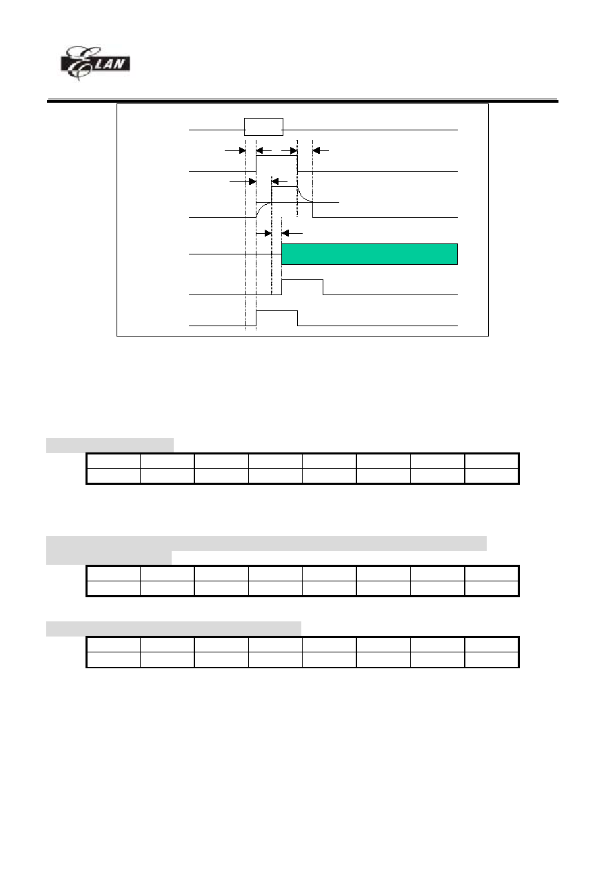
To provide the code corresponding to the last valid tone-pair received (see code table). STD signal which
steering output presents a logic high when a received tone-pair has been registered and the Q4 ~ Q1 output latch
updated and generate a interruption (IOCF has enabled); returns to logic low when the voltage on ST/GT falls
below Vtst.
F low
F high
Key
DREN
Q4~Q1
697 1209 1
1
0001
697 1336 2
1
0010
697 1477 3
1
0011
EM78P813
8-bit OTP Micro-controller
__________________________________________________________________________________________________________________________________________________________________
* This specification is subject to change without notice.
23
2004/8/19 (V1.6)
770 1209 4
1
0100
770 1336 5
1
0101
770 1477 6
1
0110
852 1209 7
1
0111
852 1336 8
1
1000
852 1477 9
1
1001
941 1209 0
1
1010
941 1336 *
1
1011
941 1477 #
1
1100
697 1633 A
1
1101
770 1633 B
1
1110
852 1633 C
1
1111
941 1633 D
1
0000
Any Any Any 0
xxxx
(x:unknown)
Bit 4~Bit 5 : Unused
Bit 6 (STD) : Delayed steering output.
Presents a logic high when a received tone-pair has been registered and the output latch updated; returns to logic
low when the voltage on St/GT falls below V tst.
0/1 Data invalid/data valid
Be sure open main clock before using DTMF receiver circuit . A logic"0,0" applied to R5 page3 b4 and b3 will
shut down power of the device to minimize the power consumption in a standby mode. It stops functions of the filters.
In many situations not requiring independent selection of receive and pause, the simple steering circuit of is
applicable. Component values are chosen according to the following formulae:
t REC = t DP + t GTP t ID = t DA + t GTA
The value of t DP is a parameter of the device and t REC is the minimum signal duration to be recognized by the
receiver. A value for C of 0.1 uF is recommended for most applications, leaving R to be selected by the designer. For
example, a suitable value of R for a t REC of 30mS would be 300k.
Different steering arrangements may be used to select independently the guard-times for tone-present (t GTP )
and tone-absent (t GTA ). This may be necessary to meet system specifications which place both accept and reject
limits on both tone duration and inter digital pause.
Guard-time adjustment also allows the designer to tailor system parameters such as talk off and noise immunity.
Increasing t REC improves talk-off performance, since it reduces the probability that tones simulated by speech will
maintain signal condition for long enough to be registered. On the other hand, a relatively short t REC with a long t DO
would be appropriate for extremely noisy environments where fast acquisition time and immunity to drop-outs would be
required.
VDD
ST/GT
EST
VDD
R
C
Fig.16 DTMF receiver delay time control
EM78P813
8-bit OTP Micro-controller
__________________________________________________________________________________________________________________________________________________________________
* This specification is subject to change without notice.
24
2004/8/19 (V1.6)
TONE
TONE
EST
ST/GT
Vtst
1/2 VDD
Q4..Q1
STD
LINE_ENG
Tdp
5~20mS
by S/W
Tgta
30mS Typ.
Tgtp
30mS Typ.
Tpq
8 uS Typ.
Fig.17 DTMF receiver timing.
Bit 7 (CMPFLAG) : Comparator output flag
0 Input voltage < reference voltage
1 Input voltage > reference voltage
<Note>Please refer to RA page 2 comparator control register .
PAGE3 SPI Data buffer
7 6 5 4 3 2 1 0
SPIB7 SPIB6 SPIB5 SPIB4 SPIB3 SPIB2 SPIB1 SPIB0
Bit 0 ~ Bit 7 (SPIB0 ~ SPIB7) : SPI data buffer
If you write data to this register, the data will write to SPIW register. If you read this data, it will read the data
from SPIR register. Please refer to
Fig.9
R9 Port 9 I/O Data , LCD address MSB , Data ROM address ,OP , Key tone control,
PAGE0 Port 9 I/O Data
7 6 5 4 3 2 1 0
P97 P96 P95 P94 P93 P92 P91 P90
Bit 0 ~ Bit 7 (P90 ~ P97) : 8-bit PORT9 ( 0~7 ) I/O data register
User can use IOC register to define input or output each bit.
PAGE1 LCD address MSB , Data ROM address
7 6 5 4 3 2 1 0
LCDA8
DRA20
DRA19
DRA18
DRA17
DRA16
Bit 0 ~ Bit 4 (DRA16 ~ DRA20) : Data ROM address(16~20) for ROM reading..
Bit 5~Bit 6 : Unused
Bit 7 (LCDA8) : MSB of LCD address for internal LCD RAM reading or writing
Other LCD address bits LCDA7 ~ LCDA0 are set from RA PAGE1 Bit 7 ~ Bit 0.
For LCD address access over 0xFFH, set this bit to "1"; otherwise set this bit to "0".
EM78P813
8-bit OTP Micro-controller
__________________________________________________________________________________________________________________________________________________________________
* This specification is subject to change without notice.
25
2004/8/19 (V1.6)
PAGE2 OP input control Register, FSK/CW/DTMF Power select
7 6 5 4 3 2 1 0
PCTRL1
PCTRL0 ADCS3
ADCS2
ADCS1
- - -
Bit 0 ~ Bit 2 : Unused.
Bit 3 ~ Bit 5(ADCS1 ~ ADCS3) : PORT65 ~ PORT67 normal IO or CMP input control bit.
ADCSX = 1 Comparator input
ADCSX = 0 normal IO
Bit 6~Bit 7 (PCTRL0~PCTRL1) : FSK,CW and DTMF receiver power control bits
PCTRL1 PCTRL0
Select
Relation
Register
0
0
FSK and DTMFr power off
-
0
1
FSK power on
RA PAGE0
1
0
DTMF receiver power on
R8 PAGE2
1 1
Can not used
*Please do not set 1 to both the bits, or FSK and DTMFr function will fail..
*When User turn on DTMF receiver power, PORT60 and PORT61 will switch to /STGT and
EST pin.
PAGE3 KEY Tone Control
7 6 5 4 3 2 1 0
URT8 URR8 DA1 DA0 URINV
KT1 KT0 KTS
Bit 0 (KTS) : Key tone output switch
0 normal PORT76
1 key tone output .
Bit 1 ~ Bit 2 (KT0 ~ KT1) : Key tone output frequency and its power control
KT1
KT0 Key tone frequency and power
0
0
32.768KHz/32 = 1.024kHz clock and enable
0
1
32.768KHz/16 = 2.048kHz clock and enable
1
0
32.768KHz/8 = 4.096kHz clock and enable
1
1
Power off key tone
Bit 3(URINV) : Enable UART TXD, RXD port inverse output
0 Disable UART TXD, RXD port inverse output
1 Enable UART TXD, RXD port inverse output
Bit 4 ~ Bit 5(DA0~DA1) :These two bits are the least significant 2 bits of Current DA. Combine R6 PAGE3 and
these 2 bits as complete 10 bits Current DA output data.
Bit 6(URR8) : MSB of UART receiver data buffer.
Bit 7(URT8) : MSB of UART transmitter data buffer.
RA CPU Power saving , main CLK select , FSK , WDT timer , LCD address
Comparator control , Tone1 generator
PAGE0 Power saving , main CLK select , FSK , WDT timer
7 6 5 4 3 2 1 0
0
PLLEN
CLK1 CLK0 ROMRI FSKDATA
/CD WDTEN
Bit 0 (WDTEN) : Watch dog control register
User can use WDTC instruction to clear watch dog counter. The counter 's clock source is 32768/2 Hz. If the
prescaler assigns to TCC. Watch dog will time out by (1/32768 )*2 * 256 = 15.616ms. If the prescaler assigns to
WDT, the time of time out will be more times depending on the ratio of prescaler.
0/1 disable/enable
EM78P813
8-bit OTP Micro-controller
__________________________________________________________________________________________________________________________________________________________________
* This specification is subject to change without notice.
26
2004/8/19 (V1.6)
Bit 1 (/CD) : FSK carrier detect indication
0/1 Carrier Valid/Carrier Invalid
It's a read only signal. If FSK decoder detect the energy of mark or space signal. The Carrier signal will go to
low level. Otherwise it will go to high.. Note!! Should be at normal mode.
Bit 2 (FSKDATA) : FSK decoding data output
It's a read only signal. If FSK decode the mark or space signal , it will output high level signal or low level
signal at this register. It's a raw data type. That means the decoder just decode the signal and has no process on
FSK signal. Note!! Should be at normal mode.
User can use FSK data falling edge interrupt function to help data decoding.
Example:
MOV A,@01000000
IOW
IOCF
;enable
FSK
interrupt
function
CLR RF
ENI
;wait for FSK data's falling edge
:
0 = Space data ( 2200Hz )
1 = Mark data (1200Hz)
FSK block power is controlled by R5 page3 bit3,4. When PCTRI1=0 and PCTRL0=1 , FSK power on.
The relation between R5 bit3 to bit4 and RA bit1 to bit 2 are show in
Fig.14. You have to power FSK decoder
up first, then wait a setup time (Tsup) and check carrier signal (/CD). If the carrier is low, program can process the
FSK data.
TIP/RING
/CD
FSKDATA
FIRST RING
2 SECONDS
0.5 SEC
0.5 SEC
SECOND RING
2 SECONDS
DATA
Tcdl
PCTRL0
Tdoc
Tcdh
Tsup
FSK signal
PCTRL1
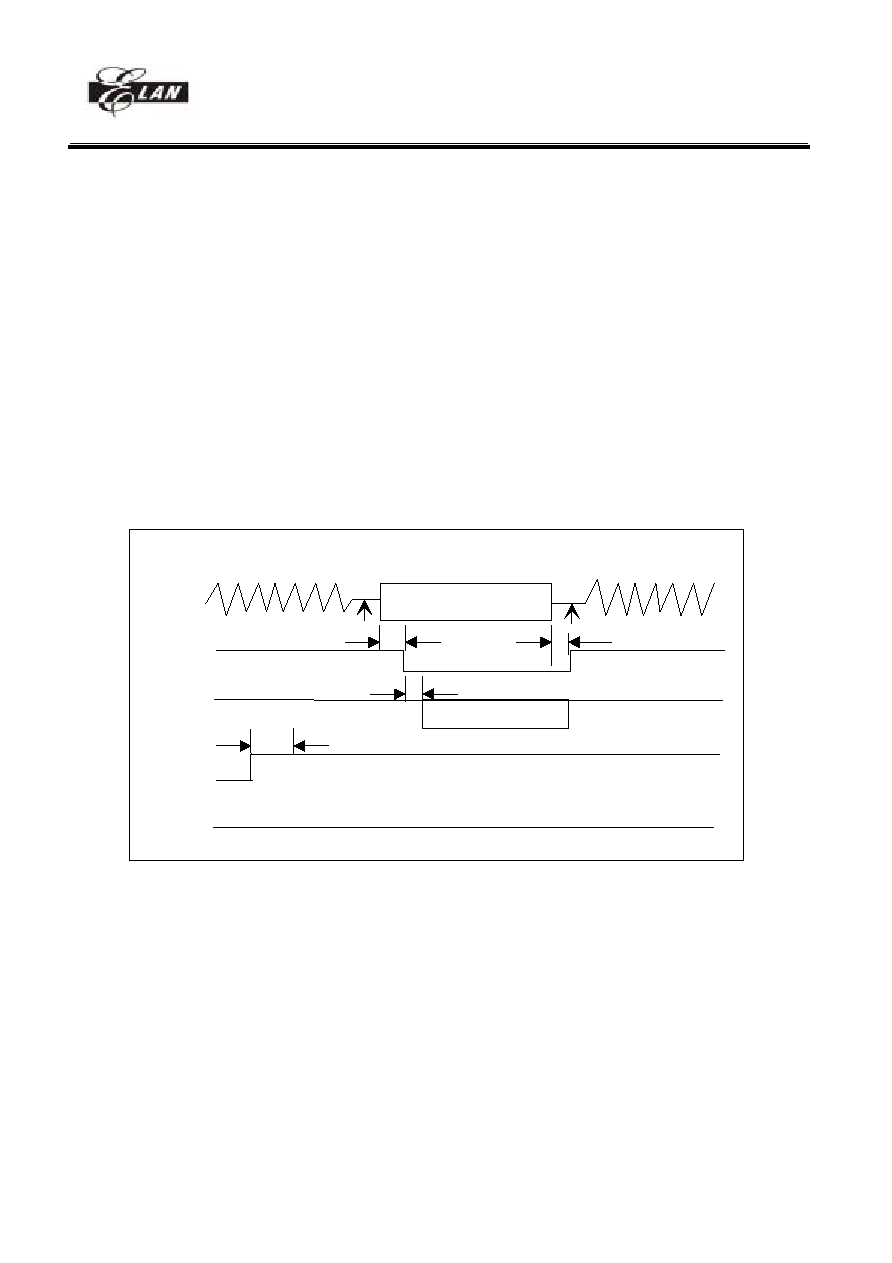
Fig.18 The relation between R5 bit3 to bit4 and RA bit1 to bit 2
The controller is a CMOS device designed to support the Caller Number Deliver feature which is offered by the
Regional Bell Operating Companies. The FSK block comprises one path: the signal path. The signal path consist of an
input differential buffer, a band pass filter, an FSK demodulator and a data valid with carrier detect circuit.
In a typical application, user can use his own external ring detect output as a triggering input to IO port. User
can use this signal to wake up whole chip by external ring detect signal. By setting "0,1" to R5 b4 and b3 (PCTRL1 &
PCTRL0) of register RA to activate the block of FSK decoder. If b4 and b3 of register R5 is set to "0,1", the block of
FSK decoder will be powered down.
The input buffer accepts a differential AC coupled input signal through the TIP and RING input and feeds this signal
to a band pass filter. Once the signal is filtered, the FSK demodulator decodes the information and sends it to a post filter.
The output data is then made available at bit 2 (FSKDATA) of register RA. This data, as sent by the central office, includes
the header information (alternate "1" and "0") and 150 ms of marking which precedes the date, time and calling number. If
EM78P813
8-bit OTP Micro-controller
__________________________________________________________________________________________________________________________________________________________________
* This specification is subject to change without notice.
27
2004/8/19 (V1.6)
no data is present, the bit 2 (DATA) of register RA is held on "1" state. This is accomplished by an carrier detect circuit
which determines if the in-band energy is high enough. If the incoming signal is valid, bit 1 (/CD) of register RA will be
"0" otherwise it will be held on "1". And thus the demodulated data is transferred to bit 2 (DATA) of register RA. If it is
not, then the FSK demodulator is blocked.
Bit 3 (ROMRI) : External Data ROM read data address auto_increase enable.
RO_IDEN ROMRI
Result
0
X
Regardless Read/Write external Data ROM,
Address flag cannot increase or decrease.
1
0
Address flag will auto_increase or decrease
after Read/Write external Data ROM
1
1
Address flag will auto_increase or decrease
after Write external Data ROM, but address
flag is constant after read external Data ROM.
Bit 4 ~ Bit 5 (CLK0 ~ CLK1) : Main clock selection bits
User can choose different frequency of main clock by CLK1 and CLK2. All the clock selection is list below.
PLLEN
CLK1
CLK0
Sub clock
MAIN clock
CPU clock
1 0 0
32.768kHz
5.374MHz
5.374MHz
(Normal
mode)
1 0 1
32.768kHz
1.7913MHz
1.7913MHz
(Normal
mode)
1 1 0
32.768kHz
10.7479MHz 10.7479MHz
(Normal
mode)
1 1 1
32.768kHz
3.5826MHz
3.5826MHz
(Normal
mode)
0
Don't care don't care
32.768kHz
Don't care
32.768kHz (Green mode)
0
Don't care don't care
32.768kHz
Don't care
32.768kHz (Green mode)
0
Don't care don't care
32.768kHz
Don't care
32.768kHz (Green mode)
0
Don't care don't care
32.768kHz
Don't care
32.768kHz (Green mode)
Bit 6 (PLLEN) : PLL enable control bit
It is CPU mode control register. If PLL is enabled, CPU will operate at normal mode (high frequency , main
clock); otherwise, it will run at green mode (low frequency, 32768 Hz).
0/1 disable/enable
Sub-clock
32.768kHz
PLL
switch
0
ENPLL
CLK1 ~ CLK0
1
System clock
3.5826MHz to analog circuit
=>5.374MHz
=>1.7913MHz
=>3.5826MHz
=>10.7479MHz
1.5
2
3
�
1
�
�
�
Fig.19 The relation between 32.768kHz and PLL
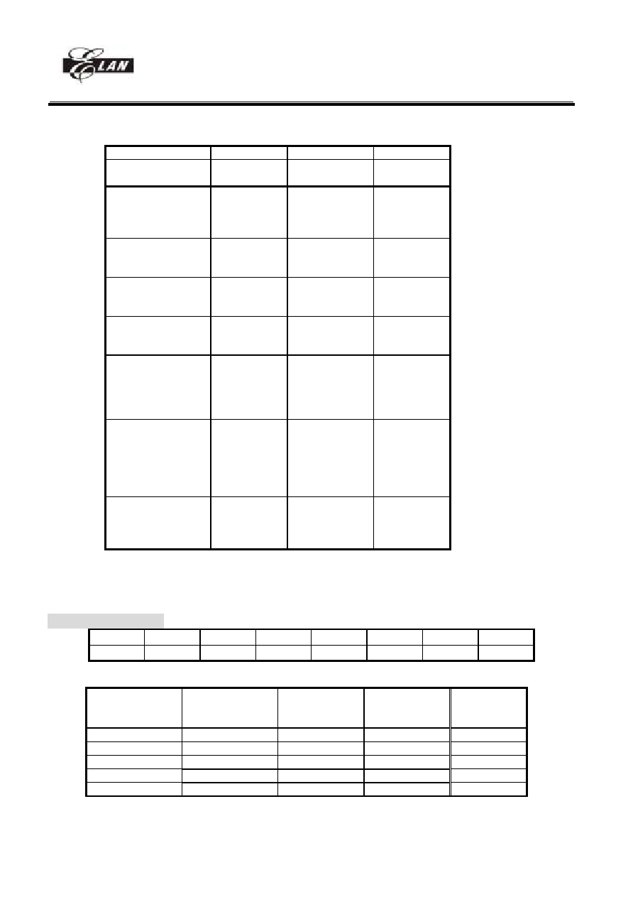
EM78P813
8-bit OTP Micro-controller
__________________________________________________________________________________________________________________________________________________________________
* This specification is subject to change without notice.
28
2004/8/19 (V1.6)
Bit 7: Unused register. Always keep this bit to 0 or some un-expect error will happen!
The status after wake-up and the wake-up sources list as the table below.
Wakeup signal
SLEEP mode
GREEN mode
NORMAL mode
RA(7,6)=(0,0)
+ SLEP
RA(7,6)=(x,0)
no SLEP
RA(7,6)=(x,1)
no SLEP
TCC time out
IOCF bit 0=1
And "ENI"
No function
Interrupt
(jump to address 8
at page0)
Interrupt
(jump to address
8 at page0)
COUNTER1 time out
IOCF bit 1=1
And "ENI"
No function
Interrupt
(jump to address 8
at page0)
Interrupt
(jump to address
8 at page0)
COUNTER2 time out
IOCF bit 2=1
And "ENI"
No function
Interrupt
(jump to address 8
at page0)
Interrupt
(jump to address
8 at page0)
WDT time out
RESET and
Jump to address
0
RESET and Jump
to address 0
RESET and
Jump to address
0
PORT7
Any one bit in IOCE
page0 = 1
And "ENI"
RESET and
Jump to address
0
Interrupt
(jump to address 8
at page0)
Interrupt
(jump to address
8 at page0)
DED interrupt
IOCE page1 bit 6 = 1
And RF bit3 logic level
variation
(switch by EDGE bit)
And "ENI"
No function
Interrupt
(jump to address 8
at page0)
Interrupt
(jump to address
8 at page0)
Stack overflow
IOC5 page1 bit7=1
& RF bit 4: 0 1
And "ENI"
No function
Interrupt
(jump to address 8
at page0)
Interrupt
(jump to address
8 at page0)
<Note> Stack overflow interrupt function is exist in ROM less and OTP chip only.
<Note> PORT70 ~ PORT76 's wakeup function is controlled by IOCE PAGE0 bit 0~bit 6 and ENI instruction. They
are falling edge trigger.
PORT77 's wakeup function is controlled by IOCE PAGE0 bit 7 . It can be trigger in falling edge or rising
edge (controlled by CONT register).
PAGE1 LCD address
7 6 5 4 3 2 1 0
LCDA7 LCDA6
LCDA5 LCDA4
LCDA3
LCDA2
LCDA1 LCDA0
Bit 0 ~ Bit 7 (LCDA0 ~ LCDA7) : LCD address for internal LCD RAM reading or writing
The data in the internal LCD RAM correspond to the COMMON and SEGMENT signals as the table .
COM31 ~ COM24
(set R9 PAGE1
bit7=1)
COM23 ~ COM16
(set R9 PAGE1
bit7=1)
COM15 ~COM8
(set R9 PAGE1
bit7=0)
COM7 ~ COM0
(set R9 PAGE1
bit7=0)
Address 180H
Address 100H
Address 080H
Address 000H
SEG0
Address 181H
Address 101H
Address 081H
Address 001H
SEG1
Address 182H
Address 102H
Address 082H
Address 002H
SEG2
: : :
:
:
: : :
:
:

EM78P813
8-bit OTP Micro-controller
__________________________________________________________________________________________________________________________________________________________________
* This specification is subject to change without notice.
29
2004/8/19 (V1.6)
: : :
:
:
Address 1EEH
Address 16EH
Address 0EEH
Address 06EH
SEG110
Address 1EFH
Address 16FH
Address 0EFH
Address 06FH
SEG111
Address 1F0H
Address 170H
Address 0F0H
Address 070H
Empty
: : :
:
:
Address 1FFH
Address 17FH
Address 0FFH
Address 07FH
Empty
PAGE2 Comparator control Register
7 6 5 4 3 2 1 0
CMPEN CMPREF CMPS1 CMPS0
CMPB3 CMPB2 CMPB1 CMPB0
If user define PORT63 , PORT64 or PORT65 (by CMPIN1, CMPIN2, CMPIN3 at R9 page2) as a comparator input or
PORT6. User can use this register to control comparator's function.
Bit 0~Bit 3(CMPB0 ~ CMPB3) : Reference voltage selection of internal bias circuit for
comparator.
Reference voltage for comparator = VDD x ( N + 0.5 )/ 16 , N = 0 to 15
Bit 4~Bit 5(CMPS0~CMPS1) : Channel selection from CMP1 to CMP3 for comparator
CMPS1 CMPS0
Input
0 0
CMP1
0 1
CMP2
1 0
CMP3
1 1 Reserved
Bit 6(CMPREF) : Switch for comparator reference voltage type
0 internal reference voltage
1 external reference voltage
Bit 7(CMPEN) : Enable control bit of comparator.
0/1 disable/enable, When CMPEN bit set to "0" , 2.0V ref circuit will powered off.
The relation between these registers shown in Fig.20.
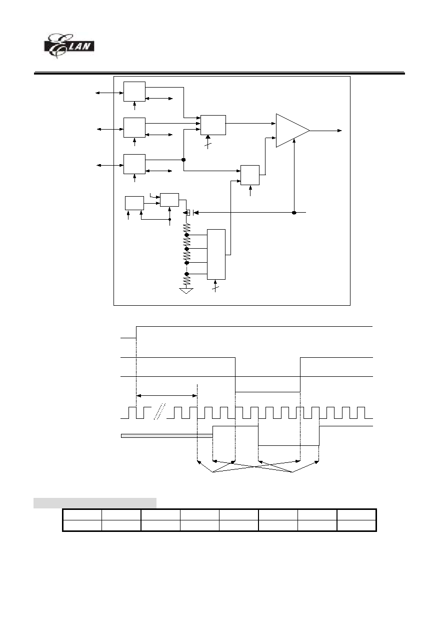
EM78P813
8-bit OTP Micro-controller
__________________________________________________________________________________________________________________________________________________________________
* This specification is subject to change without notice.
30
2004/8/19 (V1.6)
PORT65
MUX
CMP1
ADCS1
PORT66
MUX
CMP2
ADCS2
PORT67
MUX
CMP3
ADCS3
MUX
CMPS1
CMPS0
+
-
MUX
CMPREF
CMPFLAG
CMPEN
0
1
2
P65/CMP1
P66/CMP2
P67/CMP3
MUX
1/2R
R
R
1/2R
4
CMPB3 to CMPB0
1111
1110
0000
VRSEL
MUX
V2_0
ref.
2.0V
VDD
CMPEN
VR
Fig.20 Comparator circuit
CMPEN
CMP1 to CMP3
reference
voltage
CPU clock
CMPFLAG
Setup time 10us
Compare start
Compare end
Fig.21 Comparator timing
PAGE3 Tone 1 Control Register
7 6 5 4 3 2 1 0
T17 T16 T15 T14 T13 T12 T11 T10
Bit 0~Bit 7(T10~T17) : Tone generator1 frequency
divider and power control
Please Run in Normal mode .
EM78P813
8-bit OTP Micro-controller
__________________________________________________________________________________________________________________________________________________________________
* This specification is subject to change without notice.
31
2004/8/19 (V1.6)
Clock source = 85300Hz
T17~T10 = `11111111' Tone generator1 will has 334(85300/255) Hz SIN wave output.
:
:
T17~T10 = `00000010' Tone generator1 will has 41150(85300/2) Hz SIN wave output.
T17~T10 = `00000001' DC bias voltage output
T17~T10 = `00000000' Power off
Built-in tone generator can generate dialing tone signals for telephone of dialing tone type or just a single tone.
In DTMF application, there are two kinds of tone. One is the group of row frequency (TONE1), the other is the group
of column frequency (TONE2), each group has 4 kinds of frequency, user can get 16 kinds of DTMF frequency totally.
Tone generator contains a row frequency sine wave generator for generating the DTMF signal which selected by RA
page3 and a column frequency sine wave generator for generating the DTMF signal which selected by RB page3. This
block can generate single tone by filling one of these two register.
If all the values are low, the power of tone generators will turn off .
TONE2 (RB page3) High group freq.
1201.4Hz
(0X47)
1332.8Hz
(0X40)
1470.7Hz
(0X3A)
1640.4Hz
(0X34)
TONE1(RA
page3)
699.2Hz(0x07A)
1 2 3 A
768.5Hz(0x06F)
4 5 6 B
Low group freq.
853.0Hz(0x064)
7
8
9
C
937.4Hz(0x05B)
* 0 # D
Also TONE1 and TONE2 are an asynchronous tone generator so the both can be used to generate Caller ID FSK
signal. In FSK generator application, TONE1 or TONE2 can generate 1200Hz Mark bit and 2200Hz Space bit for
Bell202 or 1300Hz Mark bit and 2100Hz Space bit for V.23. See the following table.
TONE1(IOCC PAGE1) or
TONE2(IOCD PAGE1)
Freq. (Hz)
meaning
0x47
1201.4
Bell202 FSK Mark bit
0x27 2187.2
Bell202 FSK Space bit
0x42
1292.4
V.23 FSK Mark bit
0x29
2080.5
V.23 FSK Space bit
Tone generator can also generate CW or SMS signal. See the following table.
TONE1(IOCC PAGE1) or
TONE2(IOCD PAGE1)
Freq. (Hz)
meaning
0x28 2132.5
CAS
freq
0x1F 2751.6
CAS
freq
RB Port B I/O Data , LCD Data buffer , Key strobe , Tone 2 generator
PAGE0 Port B I/O Data
7 6 5 4 3 2 1 0
PB7 PB6 PB5 PB4 PB3 PB2 PB1 PB0
Bit 0 ~ Bit 7 (PB0 ~ PB7) : 8-bit PORTB ( 0~7 ) I/O data register
User can use IOC register to define input or output each bit.
EM78P813
8-bit OTP Micro-controller
__________________________________________________________________________________________________________________________________________________________________
* This specification is subject to change without notice.
32
2004/8/19 (V1.6)
PAGE1 LCD Data buffer
7 6 5 4 3 2 1 0
LCDD7 LCDD6
LCDD5 LCDD4
LCDD3
LCDD2
LCDD1 LCDD0
Bit 0 ~ Bit 7 (LCDD0 ~ LCDD7) : LCD data buffer for LCD RAM reading or writing
Example.
MOV A,@0
MOV R9_PAGE1,A
MOV RA_PAGE1,A
;ADDRESS
MOV A,@0XAA
MOV RB_PAGE1,A
;WRITE DATA 0XAA TO LCD RAM
MOV A,RB_PAGE1
;READ DATA FROM LCD RAM
:
PAGE2 KEY Strobe Control Register
7 6 5 4 3 2 1 0
STRB7 STRB6
STRB5 STRB4
STRB3
STRB2
STRB1 STRB0
Bit 0 ~ Bit 7 (STRB0 ~ STRB7) : Key strobe control bits
These key strobe control registers correspond to SEGMENT50 ~ SEGMENT57 or Port80 ~ Port87 (decided by
CHIPSEL pin). Please refer KEYSTOBE explanation (RE page3).
PAGE3 Tone 2 Control Register
7 6 5 4 3 2 1 0
T27 T26 T25 T24 T23 T22 T21 T20
Bit 0~Bit 7(T20~T27) : Tone generator1`s frequency divider and power control. Please refer to RA
Page3 Tone1 control register for detail.
RC Port C I/O Data , Data RAM data buffer , Tone 2 generator
PAGE0 Port C I/O Data
7 6 5 4 3 2 1 0
PC7 PC6 PC5 PC4 PC3 PC2 PC1 PC0
Bit 0 ~ Bit 7 (PC0 ~ PC7) : 8-bit PORTC ( 0~7 ) I/O data register
User can use IOC register to define input or output each bit.
PAGE1 Data RAM data buffer1
7 6 5 4 3 2 1 0
RAM1D7 RAM1D6 RAM1D5 RAM1D4 RAM1D3 RAM1D2 RAM1D1 RAM1D0
Bit 0 ~ Bit 7 (RAM1D0 ~ RAM1D7) : Data RAM data buffer1 for RAM reading or writing.
Example.
MOV A,@1
MOV RD_PAGE1,A
MOV A,@0
MOV RE_PAGE1,A
MOV A,@0x55
MOV RC_PAGE1,A
;write data 0x55 to DATA RAM which address is "0001".
MOV A,RC_PAGE1
;read data
:
EM78P813
8-bit OTP Micro-controller
__________________________________________________________________________________________________________________________________________________________________
* This specification is subject to change without notice.
33
2004/8/19 (V1.6)
PAGE2 KEY Strobe Control Register
7 6 5 4 3 2 1 0
STRB15 STRB14 STRB13 STRB12 STRB11 STRB10
STRB9 STRB8
Bit 0 ~ Bit 7 (STRB8 ~ STRB15) : Key strobe control bits
These key strobe control registers correspond to SEGMENT58 ~ SEGMEN65 or Port90 ~ Port97 (decided by
CHIPSEL pin). Please refer KEYSTOBE explanation (RE page3).
PAGE3 Undefined Register
7 6 5 4 3 2 1 0
0 0 0 X 0 0 0 0
Bit 0~3, 5~7: Undefined register. These bits must keep to 0.
RD PORT D I/O Data , Data RAM address , LCD control
PAGE0 PORT D I/O Data , Data RAM address
7 6 5 4 3 2 1 0
PD7 PD6 PD5 PD4 PD3 PD2 PD1 PD0
Bit 0 ~ Bit 7 (PD0 ~ PD7) : 7-bit PORTD ( 0~6 ) I/O data register
User can use IOC register to define input or output each bit.
PAGE1 Data RAM Address1(Low 8 bits)
7 6 5 4 3 2 1 0
RAM1A7 RAM1A6 RAM1A5 RAM1A4 RAM1A3 RAM1A2 RAM1A1 RAM1A0
Bit 0~Bit 7 (RAM1A0 ~ RAM1A7) : Data RAM address1 (address0 to address7) for RAM reading or writing
PAGE2 LCD Control Register
7 6 5 4 3 2 1 0
-
IRS1 IRS0 Bias4 Bias3 Bias2 Bias1 Bias0
Bit 0 ~ Bit 4 (Bias0 ~ Bias4) : LCD operation voltage selection
About the relation with VDD and V1 , please refer
Fig.20 and 21.
(Bias4 to Bias0)
VEV voltage
V1(1+Rb/Ra ratio = 2)
00000
Vref * (1-2/100)
5.29V
00001
Vref * (1-3/100)
5.24V
00010
Vref * (1-4/100)
5.18V
00011
Vref * (1-5/100)
5.13V
00100
Vref * (1-6/100)
5.08V
: : :
11101
Vref * (1-31/100)
3.73V
11110
Vref * (1-32/100)
3.67V
11111
Vref * (1-33/100)
3.62V
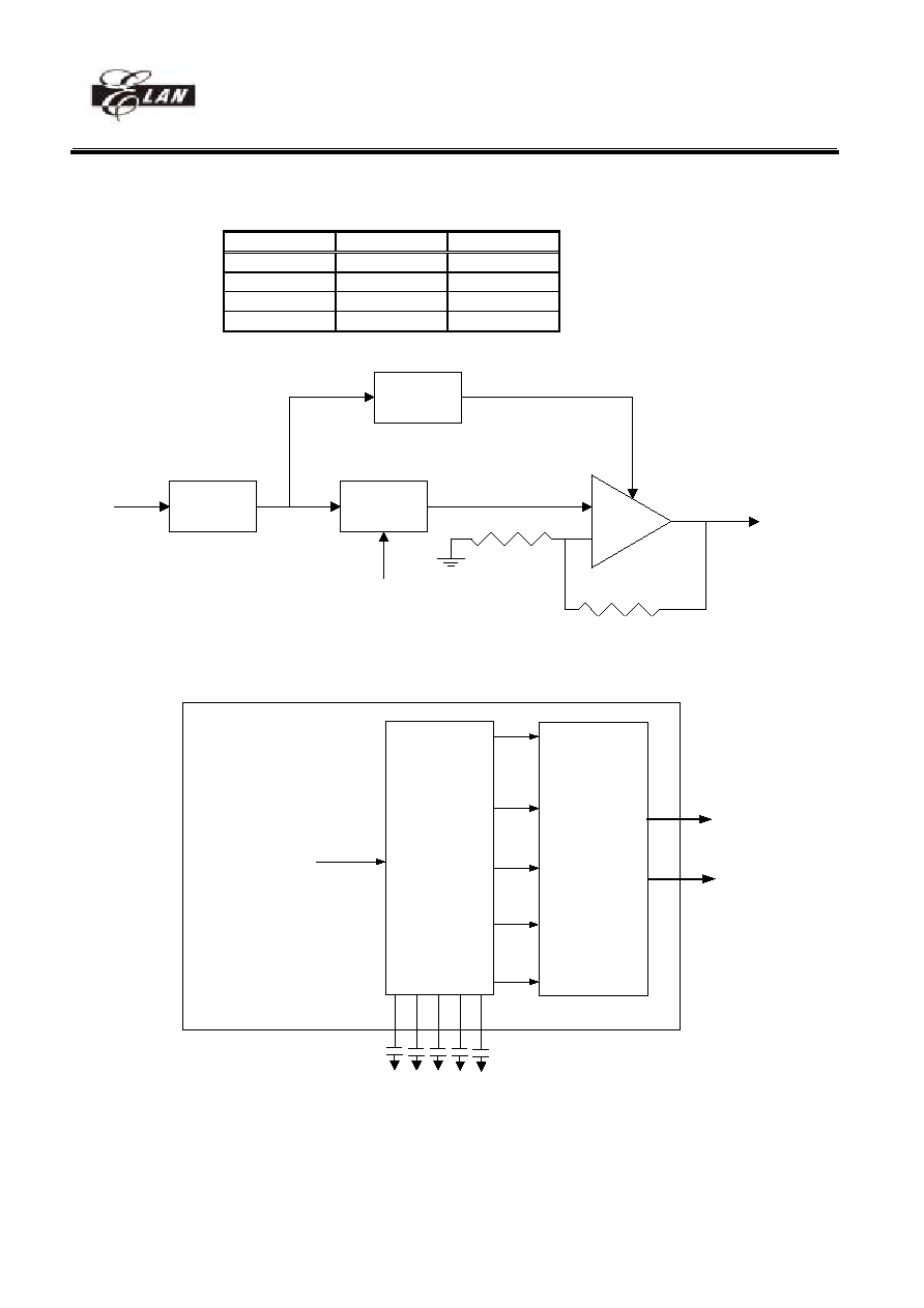
EM78P813
8-bit OTP Micro-controller
__________________________________________________________________________________________________________________________________________________________________
* This specification is subject to change without notice.
34
2004/8/19 (V1.6)
Bit 5~ Bit 6 (IRS0~IRS1) : Internal regulator resister ratio modulate .
LCD driver bias voltage V1 = 2.7V x (1-Bias/100) x IRS rate ; If V1 larger than 5.4V,V1 will limit to 5.4V.
IRS1 IRS0
(1+Rb/Ra)
ratio
0 0 1.5
0 1
1.75
1 0 2.0
1 1
2.25
BIAS
Circuit
Vref = 2.7V
Regulator
Circuit
VDD
Charge
pump Circuit
( Vref x 2 )
Bias4 ~ Bias 0
VEV = 1.805V ~ 2.65V
+
-
Vout = 5.4V
V1 = VEV*(1+Rb/Ra)
Ra
Rb
Vsat = 5.3V
Fig.23 The relation between VDD and V1
VC1 ~ VC5
VC1 ~ VC5
Bias
generator
LCD driver
for
COM and SEG
COMs
SEGs
V1
Fig.24 The relation between BIAS and VC1 ~ VC5
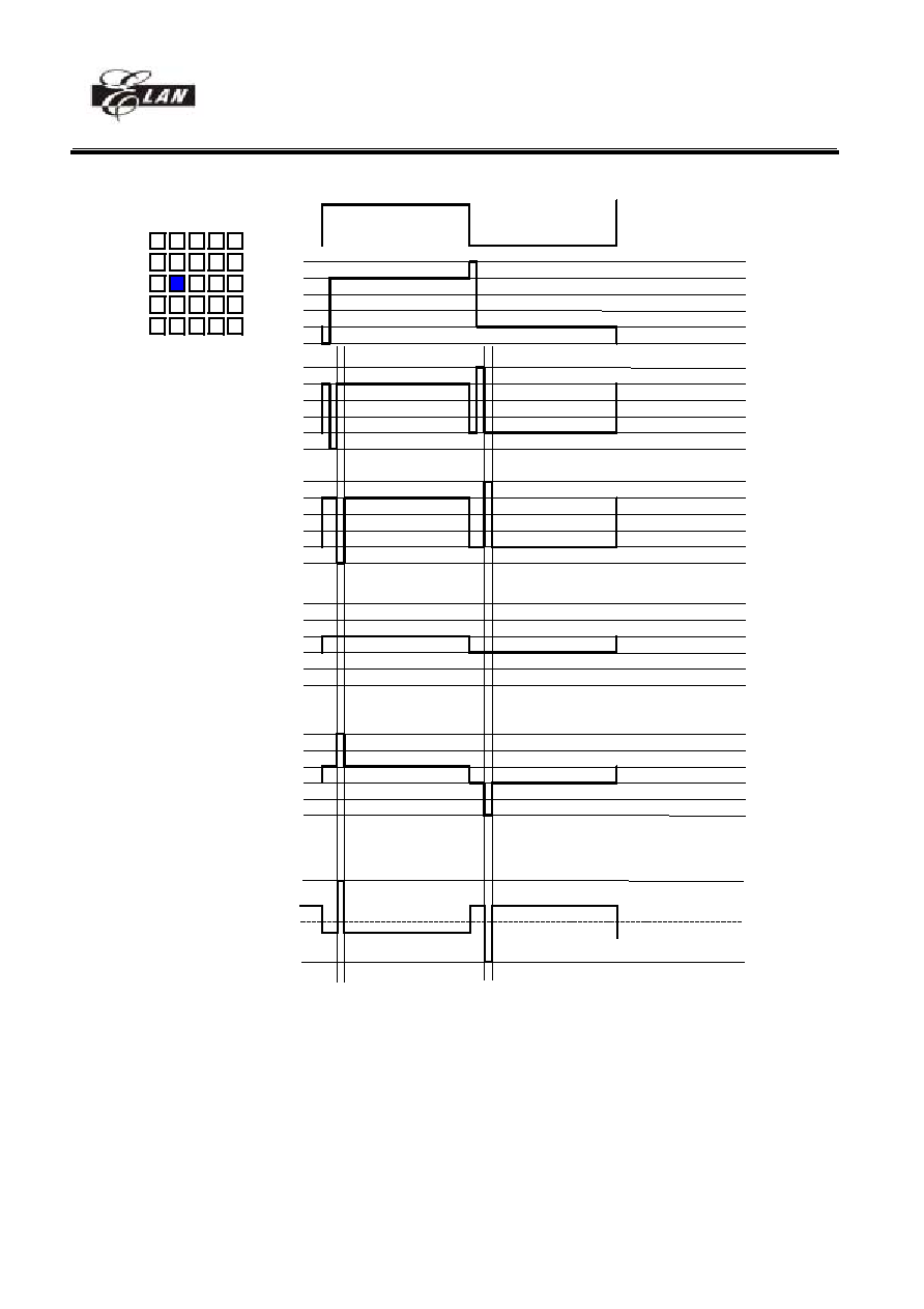
EM78P813
8-bit OTP Micro-controller
__________________________________________________________________________________________________________________________________________________________________
* This specification is subject to change without notice.
35
2004/8/19 (V1.6)
frame
COM 0
COM 1
COM 2
SEG 0
SEG 1
VC1
Gnd
VC2
VC3
VC4
VC5
VC1
Gnd
VC2
VC3
VC4
VC5
VC1
Gnd
VC2
VC3
VC4
VC5
VC1
Gnd
VC2
VC3
VC4
VC5
VC1
Gnd
VC2
VC3
VC4
VC5
SEG 1 - COM 2
VC1
-VC1
VSS
COM 0
COM 1
COM 2
:
:
SEG 0
SEG 1
:
:
Fig.25 1/5,1/6,1/7 bias LCD COMMON and SEGMENT waveform
Bit 7 : Unused
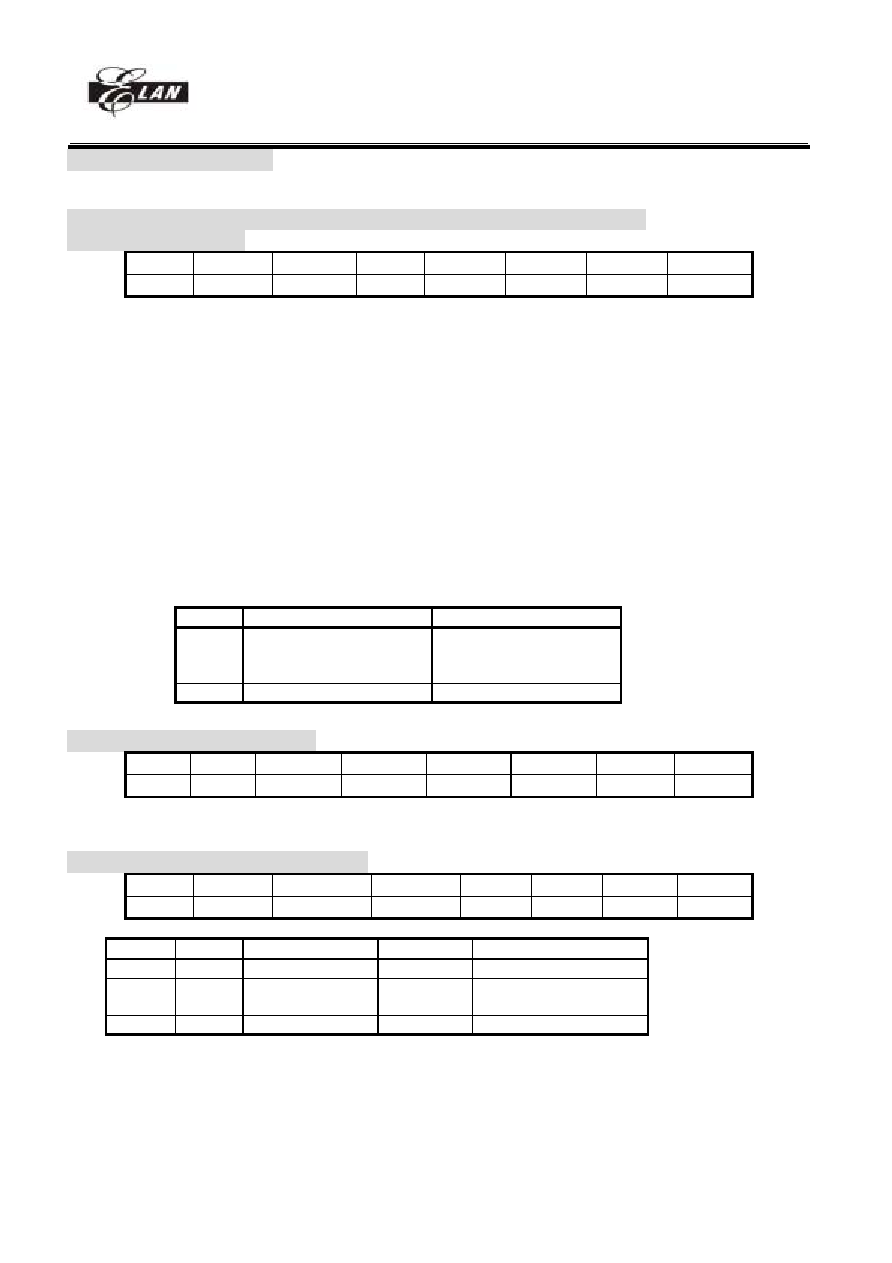
EM78P813
8-bit OTP Micro-controller
__________________________________________________________________________________________________________________________________________________________________
* This specification is subject to change without notice.
36
2004/8/19 (V1.6)
PAGE3 Undefined register
This register is not allowed to used.
RE Interrupt flag1 , Data RAM address1(H) CAS , LCD Control , Key Scan ,
PAGE0 Interrupt flag1
7 6 5 4 3 2 1 0
INT7 INT6 INT5 INT4 INT3 INT2 INT1 INT0
Bit 0 (INT0) : External INT0 pin interrupt flag
If PORT70 has a falling edge trigger signal. CPU will set this bit.
Bit 1 (INT1) : External INT1 pin interrupt flag
If PORT71 has a falling edge trigger signal. CPU will set this bit.
Bit 2 (INT2) : External INT2 pin interrupt flag
If PORT72 has a falling edge trigger signal. CPU will set this bit.
Bit 3 (INT3) : External INT3 pin interrupt flag
If PORT73 has a falling edge trigger signal. CPU will set this bit.
Bit 4 (INT4) : External INT4 pin interrupt flag
If PORT74 has a falling edge trigger signal. CPU will set this bit.
Bit 5 (INT5) : External INT5 pin interrupt flag
If PORT75 has a falling edge trigger signal. CPU will set this bit.
Bit 6 (INT6) : External INT6 pin interrupt flag
If PORT76 has a falling edge trigger signal. CPU will set this bit.
Bit 7 (INT7) : External INT7 pin interrupt flag
If PORT77 has a falling (or rising and falling) edge trigger signal. CPU will set this bit.
Signal Trigger
<Note>
INT0
:
INT6
Falling edge
INT7
Falling/Falling & rising edge Controlled by CONT register
PAGE1 Data RAM Address1(H)
7
6 5 4 3 2 1 0
RAM1A13 RAM1A12 RAM1A11 RAM1A10 RAM1A9 RAM1A8
Bit 0~Bit 5(RAM1A8 ~ RAM1A13) : Data RAM address (address8 to address13) for RAM reading.
Bit 6~Bit 7 : Unused
PAGE2 CAS , LCD Control , Key Scan
7 6 5
4 3 2 1 0
CAS
KEYSTROB KEYSCAN LCD1
LCD0
LCDM1
LCDM0
Bit 0~Bit 1(LCDM0~LCDM1) : LCD common mode, bias select and COM/SEG switch control bits
LCDM1 LCDM0 COM output mode
LCD bias
COM/SEG switch
0
0
32 common
1/7
COM 16 ~ COM 31 select
0
1
24 common
1/6
COM 16 ~ COM 23 ,
SEG98 ~ SEG 105 select
1
X
16 common
1/5
SEG 98 ~ SEG 111 select
<Note> When 32 LCD common mode is set, COM16/SEG111 pin ~ COM31/SEG98 pin are set to COM16 ~
COM31 and LCD bias is switch 1/7 bias. When 24 LCD common mode is set, COM16 pin ~ COM23/SEG106
pin are set to COM16 ~ COM23 and COM24/SEG105 pin ~ COM31/SEG98 pin are set to SEG105 ~ SEG98.
When 16 LCD common mode is set, COM16 pin ~ COM31/SEG98 pin are set to SEG1131~ SEG98.
EM78P813
8-bit OTP Micro-controller
__________________________________________________________________________________________________________________________________________________________________
* This specification is subject to change without notice.
37
2004/8/19 (V1.6)
Bias VC1 VC2 VC3 VC4 VC5
1/5 V1 4/5*V1 3/5*V1 2/5*V1 1/5*V1
1/6 V1 5/6*V1 4/6*V1 2/6*V1 1/6*V1
1/7 V1 6/7*V1 5/7*V1 2/7*V1 1/7*V1
Bit 2~Bit 3(LCD0~LCD1) : LCD operation function definition.
LCD1
LCD0 LCD
operation
0 0
Disable
0 1
Blanking
1 0
Reserved
1 1
LCD
enable
<Note 1> Key strobe and Key check functions should be normal operating whenever LCD is
enabled
or
disabled.
<Note 2> When LCD operation disable:
(1) Internal Voltage regulator will disable and VREF pin is into high impedance.
(2) Charge pump circuit disable.
(3) Internal non-Inverter OP Amp power off.
The controller can drive LCD directly. LCD block is made up of LCD driver, display RAM, segment output pins,
common output pins and LCD operating bias pins.
Duty is determined by
RD PAGE2 bit5.
The number of segment , the number of common and frame frequency are
determined by LCD mode register RE PAGE2 Bit 0~ Bit 1.
When 16 LCD commons and 1/4 duty are used, LCD operating bias pins VC1, VC2, VC4 and VC5 need to be
connected 0.1uF capacitors to the ground (VC3 is not necessary). When 24 and 32 LCD common is used, all LCD
operating bias pins VC1 ~ VC5 need to be connected 0.1uF capacitors to the ground.
LCD driver can be controlled as different driving ability (refer to RD PAGE2 register).
The basic structure contains a timing control which uses the basic frequency 32.768kHz to generate the proper timing
for different duty and display access. RE PAGE2 register is a command register for LCD driver and display. The LCD
display (disable, enable, blanking) is controlled by RE PAGE0 Bit 2 ~ Bit 3 and the driving duty is decided by RE
PAGE2 Bit 0 ~ Bit 1. LCD display data is stored in data RAM which address and data access controlled by registers
R9, RA PAGE1 and RB PAGE1.
User can regulate the contrast of LCD display by RD PAGE2 (BIAS4..BIAS0). Up to 32 levels contrast is convenient
for better display. And the internal voltage follower can afford large driving source.
Bit 4 (KEYSCAN) : Key scan function enable control bit
0/1 disable/enable
If you enable key scan function LCD waveform will has a small pulse within a period like fig.23
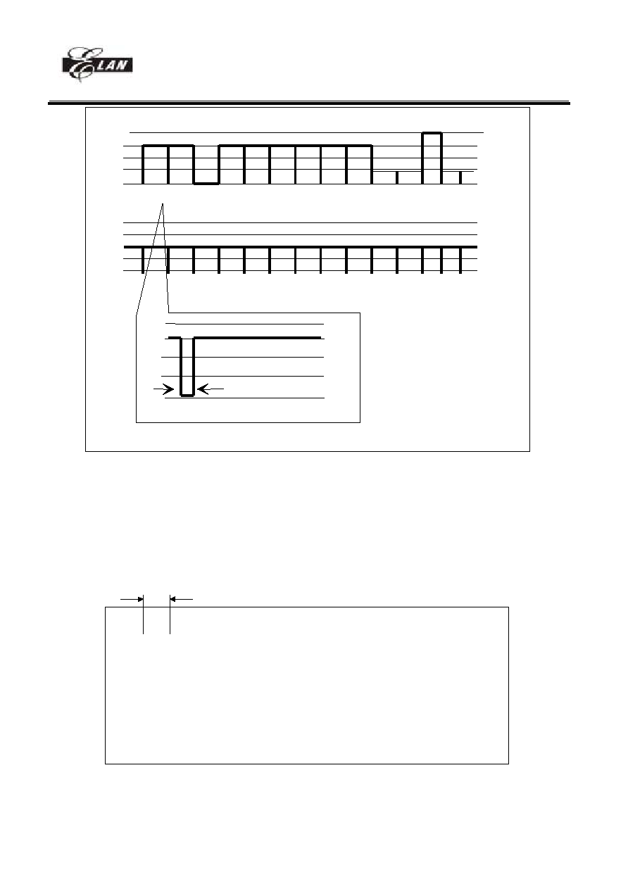
EM78P813
8-bit OTP Micro-controller
__________________________________________________________________________________________________________________________________________________________________
* This specification is subject to change without notice.
38
2004/8/19 (V1.6)
COM2
SEG
V1
V2
V4
V5
GND
30us
V1
V2
V4
V5
GND
V1
V2
V4
V5
GND
Fig.26 key scan waveform for 1/16 duty
Bit 5 (KEYSTRB) : Key strobe enable control bit
0/1 disable/enable
key strobe signal , if you set this bit , segment will switch to strobe signal temporally and output zero signal
( one instruction long ) one by one from segment 50 to segment 65. During one segment strobe time, CPU will
check port7(0:3) equal to "1111" or not. If not, CPU will latch a zero at RB PAGE1 and RC PAGE1 one by one
depends on which segment strobe. After strobe, this bit will be cleared . Fig.27 is key strobe signal.
REGISTER
RB(0) RB(1) RB(2) RB(3) RB(4) RB(5) RB(6) RB(7) RC(0) RC(1) RC(2) RC(3) RC(4) RC(5) RC(6) RC(7)
STROBE
SEG50
SEG51
SEG52
SEG53
SEG54
SEG55
SEG56
SEG57
SEG58
SEG59
SEG60
SEG61
SEG62
SEG63
SEG64
SEG65
0 1 1 1 1 1 1 1 1 1 1 1 1 1 1 1
One instruction
1 0 1 1 1 1 1 1 1 1 1 1 1 1 1 1
1 1 0 1 1 1 1 1 1 1 1 1 1 1 1 1
1 1 1 0 1 1 1 1 1 1 1 1 1 1 1 1
1 1 1 1 0 1 1 1 1 1 1 1 1 1 1 1
1 1 1 1 1 0 1 1 1 1 1 1 1 1 1 1
1 1 1 1 1 1 0 1 1 1 1 1 1 1 1 1
1 1 1 1 1 1 1 0 1 1 1 1 1 1 1 1
1 1 1 1 1 1 1 1 0 1 1 1 1 1 1 1
1 1 1 1 1 1 1 1 1 0 1 1 1 1 1 1
1 1 1 1 1 1 1 1 1 1 0 1 1 1 1 1
1 1 1 1 1 1 1 1 1 1 1 0 1 1 1 1
1 1 1 1 1 1 1 1 1 1 1 1 0 1 1 1
1 1 1 1 1 1 1 1 1 1 1 1 1 0 1 1
1 1 1 1 1 1 1 1 1 1 1 1 1 1 0 1
1 1 1 1 1 1 1 1 1 1 1 1 1 1 1 0
Fig.27 key strobe signal

EM78P813
8-bit OTP Micro-controller
__________________________________________________________________________________________________________________________________________________________________
* This specification is subject to change without notice.
39
2004/8/19 (V1.6)
Fig.28 show the relationship between KEYSCAN, KEYSTROBE and segments.
Fig.29 is key scan flow by interrupt trigger.
RELATION BETWEEN SEGMENT , KEYSCAN, KEY STROBE
MUX
KEYSTROBE
SEG50~SEG65
KEY SCAN
CONTROL
KEY SCAN PULSE
0
1
KEY STROBE SIGNAL
Fig.28 KEYSCAN, KEYSTROBE
Set port7(3:0) input
port7 pull high
enable key scan signal
Set INT0~INT3 interrupt
ENI
Interrupt occur?
Y
N
Enable main clock (Normal mode)
program delay
Analysis external interrupt ( column key )
set strobe function
enable keystrobe
program delay
read strobe data (row key)
Get the key location
Execution
key function
Fig.29 key scan flow by interrupt trigger
Bit 6 : Unused
Bit 7 (CAS) : CALL WAITING decoding output
0/1 CW data valid / No data
EM78P813
8-bit OTP Micro-controller
__________________________________________________________________________________________________________________________________________________________________
* This specification is subject to change without notice.
40
2004/8/19 (V1.6)
PAGE3 UART transmitter data buffer
7 6 5 4 3 2 1 0
URT7 URT6 URT5 URT4 URT3 URT2 URT1 URT0
Bit 0~Bit 7(URT0~URT7) : Low 8 bit UART transmitter data buffer
RF Interrupt flag
7 6 5 4 3 2 1 0
RBF/SDT FSK/CW
-
UART
DED
CNT2
CNT1
TCC
"1" means interrupt request, "0" means non-interrupt
Bit 0 (TCC) : TCC timer overflow interrupt flag
Set when TCC timer overflows .
Bit 1 (CNT1) : Counter1 timer overflow interrupt flag
Set when counter1 timer overflows.
Bit 2 (CNT2) : Counter2 timer overflow interrupt flag
Set when counter2 timer overflows .
Bit 3 (DED) : Interrupt flag of Differential Energy Detector (DED) output data. If DEDD(RE page2 bit7) has a falling
edge signal (or falling & rising edge signal , switch by IOCE page1 bit5), CPU will set this bit.
Bit 4 (UART) : Universal Asynchronous Receiver Transmitter interrupt flag. When
transmitter buffer empty , receiver buffer full or receiver data error, this bit will be set.
Bit 5Undefined register. Note that this bit is not ensured to be a fix value.
Bit 6 (FSK/CW) : FSK data or Call waiting data interrupt flag.
If FSKDATA or CAS has a falling edge trigger signal, CPU will set this bit.
Bit 7 ( RBF/STD) : SPI data transfer complete or DTMF receiver signal valid interrupt
If serial IO 's RBF signal has a rising edge signal (RBF set to "1" when transfer data completely), CPU will set
this bit. Or DTMF receiver's STD signal has a rising edge signal (DTMF decode a DTMF signal).
IOCF is the interrupt mask register. User can read and clear.
Trigger edge as the table
Signal Trigger
<Note>
TCC Time
out
COUNTER1
Time out
8/16 bits select by CONT register
COUNTER2 Time
out
DED Signal
detect
UART
Receiver full, Transmitter
empty or error(if enable)
ADI
AD sampling success
FSK Falling
edge
RBF/STD Rising
edge
EM78813 MCU will store ACC,R3 status and R5 PAGE automatically after an interrupt is triggered.
And it will be restored after instruction "RETI".
PAGE2 External Data ROM
7 6 5 4 3 2 1 0
EXA8 EXA7 EXA6 EXA5 EXA4 EXA3 EXA2 EXA1
Bit 0~Bit 7(EXA1~EXA8) : Expanding Data ROM start address A1~A8
PAGE2 External Data ROM
7 6 5 4 3 2 1 0
EXA16 EXA15 EXA14 EXA13
EXA12
EXA11
EXA10 EXA9
Bit 0~Bit 7(EXA9~EXA16) : Expanding Data ROM start address A9~A16
EM78P813
8-bit OTP Micro-controller
__________________________________________________________________________________________________________________________________________________________________
* This specification is subject to change without notice.
41
2004/8/19 (V1.6)
PAGE3 Undefined register
This register is not allowed to used.
R10~R3F (General Purpose Register)
R10~R3F (Banks 0 ~ 3) : All of them are general purpose registers
VII.3 Special Purpose Registers
A (Accumulator)
Internal data transfer, or instruction operand holding
It's not an addressable register.
CONT ( Control Register )
7 6 5 4 3 2 1 0
INT/EDGE INT TS DAEN PAB RSR2 RSR1 RSR0
Bit 0 ~ Bit 2 (PSR0 ~ PSR2) : TCC/WDT prescaler bits
PSR2
PSR1
PSR0
TCC rate
WDT rate
0 0 0 1:2 1:1
0 0 1 1:4 1:2
0 1 0 1:8 1:4
0 1 1 1:16 1:8
1 0 0 1:32 1:16
1 0 1 1:64 1:32
1 1 0 1:128 1:64
1 1 1 1:256
1:128
Bit 3(PAB) : Prescaler assignment bit
0/1 TCC/WDT
Bit 4 (DAEN) : Current DA enable control
0/1 disable/enable
Bit 5 (TS) : TCC signal source
0/1 Instruction clock / 16.384K Hz
Instruction clock = MCU clock/2, Refer to RA Bit 4 ~ Bit 6 for PLL and Main clock selection. See Fig.15.
Bit 6 (INT) : INT enable flag
0 interrupt masked by DISI or hardware interrupt
1 interrupt enabled by ENI/RETI instructions
Bit 7(INT_EDGE) : interrupt edge type of P77
0 P77 's interruption source is a rising edge signal and falling edge signal.
1 P77 's interruption source is a falling edge signal.
CONT register is readable (CONTR) and writable (CONTW).There is an 8-bit counter available as prescaler for
the TCC or WDT. The prescaler is available for the TCC only or WDT only at the same time.
An 8 bit counter is available for TCC or WDT determined by the status of the bit 3 (PAB) of the CONT register.
See the prescaler ratio in CONT register.Fig.25 depicts the circuit diagram of TCC/WDT. Both TCC and prescaler
will be cleared by instructions which write to TCC each time. The prescaler will be cleared by the WDTC and SLEP
instructions, when assigned to WDT mode.
The prescaler will not be cleared by SLEP instructions, when assigned to TCC mode.
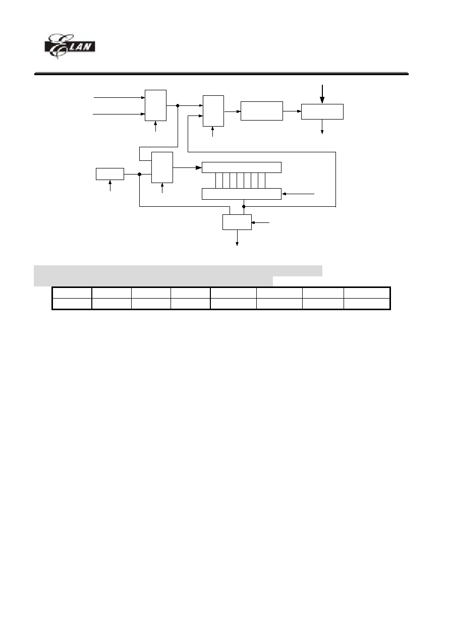
EM78P813
8-bit OTP Micro-controller
__________________________________________________________________________________________________________________________________________________________________
* This specification is subject to change without notice.
42
2004/8/19 (V1.6)
Instruction clock
M
U
X
TS
PAB
M
U
X
SYNC
2 cycles
TCC overflow interrupt
Data
Bus
TCC(R1)
PSR0 ~
PSR2
8-bit Counter
8-to-1 MUX
MUX
PAB
WDT timeout
PAB
M
U
X
WDT
WDTE
16.384kHz
Fig.30 Block diagram of TCC and WDT
IOC5 Address Automatic Increase/Decrease control , Data RAM data buffer2
PAGE0 Address Automatic Increase/Decrease control register
7 6 5 4 3 2 1 0
DA2_ID DA1_ID DO_ID LCD_ID DA2_IDEN DA1_IDEN DO_IDEN
LCD_IDEN
Bit 0 (LCD_IDEN) : Enable on_chip LCD RAM address Increase/Decrease Enable Function.
If set this bit, LCD address flag will increase or decrease after access ( read or write ) LCD data.
1/0
Enable / Disable
**EM78813 provided 32x98 dot LCD driver and it's SEGMENT address(COM0~COM7) is 0x00~0x7F(RA
PAGE1). When using 32 x 98 LCD driving mode, LCD RAM will mapping to
0x000~0x061,0x080~0x0E1,0x100~0x161 and 0x181~0x1E1. If enable on_chip LCD RAM address
auto_increase function , After access data from LCD driver in address 0x061, LCD RAM address will
auto_increase to 0x062 and it will over LCD range. User must assign address to 0x080 when LCD RAM
address point to 0x061.
Bit 2 (DO_IDEN) : Enable DATA ROM address flag Increase/Decrease Enable Function.
If set this bit, DATA ROM address will increase or decrease after access ( read or write ) DATA ROM data.
1/0
Enable / Disable
Bit 3(DA1_IDEN) : Enable DATA RAM address flag1(RD and RE register) Increase/Decrease Enable Function.
If set this bit, DATA RAM address will increase or decrease after access ( read or write ) DATA RAM data (RC
register).
1/0
Enable / Disable
Bit 4 (DA2_IDEN) : Enable DATA RAM address flag2(IOC6 and IOC7) Increase/Decrease Enable Function.
If set this bit, DATA RAM address will increase or decrease after access ( read or write ) DATA RAM data (IOC5
register).
1/0
Enable / Disable
Bit 5 (LCD_ID) : on_chip LCD RAM address automatic increase/decrease switch. Set to 1 means
auto_increase, clear to 0 means auto_decrease.
1/0 auto increase / auto decrease
Bit 6 (DO_ID) : DATA ROM address automatic increase/decrease switch. Set to 1 means
auto_increase, clear to 0 means auto_decrease.
1/0 auto increase / auto decrease
Bit 7 (DA1_ID) : DATA RAM address(RD and RE register) automatic increase/decrease switch. Set to 1 means
auto_increase, clear to 0 means auto_decrease.
EM78P813
8-bit OTP Micro-controller
__________________________________________________________________________________________________________________________________________________________________
* This specification is subject to change without notice.
43
2004/8/19 (V1.6)
1/0 auto increase / auto decrease
Bit 7 (DA2_ID) : DATA RAM address(IOC6 and IOC7 register) automatic increase/decrease switch. Set to 1 means
auto_increase, clear to 0 means auto_decrease.
1/0 auto increase / auto decrease
PAGE1 Data RAM data buffer2
7 6 5 4 3 2 1 0
RAM2D7 RAM2D6 RAM2D5 RAM2D4 RAM2D3 RAM2D2 RAM2D1 RAM2D0
Bit 0 ~ Bit 7 (RAM1D0 ~ RAM1D7) : Data RAM data buffer for RAM reading or writing.
Collocation RC~RE PAGE2 , user can move a large number continue data from an address to another in data RAM.
Example(move data from 0x0000 to 0x1000):
BC R3,@5
MOV A , @0xF0
;Enable Rata RAM flag1 and flag2 auto_increase function
IOW
0x05
BS R3 , @5
:Set correspond PAGE
BS R3 , @6
BC R3 , @7
MOV A , @0x00
;Assign DATA RAM index1 start address"0x0000"
MOV
0x0D
,
A
MOV
0x0E
,
A
IOW 0x06
; Assign DATA RAM index2 start address"0x1000"
MOV
A
,
@0x10
IOW
0x07
MOV
A
,
0x0C
;Read
data
from
index1(address:0x0000)
IOW 0x05
;Write data to index2(address:0x1000)
MOV A , 0x0C
;Read data from index1(address:0x0001)
IOW 0x05
;Write data to index2(address:0x1001)
:
:
IOC6 PORT 6 I/O Control , Data RAM address(L)
PAGE0 PORT 6 I/O Control
7 6 5 4 3 2 1 0
IOC67 IOC66 IOC65 IOC64 IOC63 IOC62 IOC61 IOC60
Bit 0~Bit 7 (IOC60 ~ IOC67) : PORT6(0~7) I/O direction control register
0 put the relative I/O pin as output
1 put the relative I/O pin into high impedance
PAGE1 Data RAM Address2(L)
7 6 5 4 3 2 1 0
RAM2A7 RAM2A6 RAM2A5 RAM2A4 RAM2A3 RAM2A2 RAM2A1 RAM2A0
Bit 0~Bit 7 (RAM2A0 ~ RAM2A7) : Data RAM address (address0 to address7) for RAM reading or writing
IOC7 PORT 7 I/O Control , Data RAM Address2(H)
PAGE0 PORT 7 I/O Control
7 6 5 4 3 2 1 0
IOC77 IOC76 IOC75 IOC74 IOC73 IOC72 IOC71 IOC70
Bit 0~Bit 7 (IOC70 ~ IOC77) : PORT7(0~7) I/O direction control register
0 put the relative I/O pin as output
1 put the relative I/O pin into high impedance
EM78P813
8-bit OTP Micro-controller
__________________________________________________________________________________________________________________________________________________________________
* This specification is subject to change without notice.
44
2004/8/19 (V1.6)
PAGE1 Data RAM address2(H)
7
6 5 4 3 2 1 0
RAM2A13
RAM2A12 RAM2A11 RAM2A10 RAM2A9
RAM2A8
Bit 0~Bit 5 (RAM2A8 ~ RAM2A13) : Data RAM address (address8 to address13) for RAM reading or writing
Bit 6~Bit 7 : Unused
IOC8 PORT 8 I/O Control ,Port8 and Port9 IO/SEG&COM Control
PAGE0 PORT 8 I/O Control
7 6 5 4 3 2 1 0
IOC87 IOC86 IOC85 IOC84 IOC83 IOC82 IOC81 IOC80
Bit 0 ~ Bit 7 (IOC80 ~ IOC87) : PORT8(0~7) I/O direction control register
0 put the relative I/O pin as output
1 put the relative I/O pin into high impedance
PAGE1 IO/SEG&COM Control Register
7 6 5 4 3 2 1 0
- -
LCDDV1 LCDDV0
P9SH
P9SL
P8SH
P8SL
Bit 0 (P8SL) : Switch low nibble I/O Port8 or LCD segment output for share pins SEGxx/P8x pins
0 select normal P80 ~ P83 for low nibble PORT8
1 select SEG66~SEG69 output for LCD SEGMENT output.
Bit 1 (P8SH) : Switch high nibble I/O Port8 or LCD segment output for share pins SEGxx/P8x pins
0 select normal P84 ~ P87 for high nibble PORT8
1 select SEG70 ~ SEG73 output for LCD SEGMENT output.
Bit 2 (P9SL) : Switch low nibble I/O Port9 or LCD segment output for share pins
0 select normal P90 ~ P93 for low nibble PORT9
1 select SEG74~SEG77 output for LCD SEGMENT output.
Bit 3 (P9SH) : Switch low nibble I/O Port9 or LCD segment output for share pins
0 select normal P94 ~ P97 for high nibble PORT9
1 select SEG78~SEG81 output for LCD SEGMENT output.
Bit 4~Bit 5(LCDDV0~LCDDV1) : LCD driver's driving ability control
LCDDV1 LCDDV0
Driving
mode
0
0
Normal mode (ratio = 1)
0
1
Weak mode (ratio = 1/2)
1
0
Strong mode (ratio = 2)
1
1
Maximum mode (ratio = 4)
LCDDV0 ~ LCDDV1 are used to select the driving ability of LCD driver. The driving ability is Maximum
mode > Strong mode > Normal mode > Weak mode by 1/2 ratio individually. The larger driving ability it is selected,
the larger output loading of LCD driver output can be afforded and the more current consumption is occurred. It
depends on user's application.
Bit 6~ Bit7: Undefined register. These two bits are not allowed to use.
IOC9 PORT9 I/O Control , Port B IO/SEG Control
PAGE0 PORT 9 I/O Control
7 6 5 4 3 2 1 0
IOC97 IOC96 IOC95 IOC94 IOC93 IOC92 IOC91 IOC90
Bit 0 ~ Bit 7 (IOC90 ~ IOC97) : PORT9(0~7) I/O direction control register
0 put the relative I/O pin as output
1 put the relative I/O pin into high impedance
EM78P813
8-bit OTP Micro-controller
__________________________________________________________________________________________________________________________________________________________________
* This specification is subject to change without notice.
45
2004/8/19 (V1.6)
PAGE1 Port B IO/SEG Control Register
7 6 5 4 3 2 1 0
PBS7 PBS6 PBS5 PBS4 PBS3 PBS2 PBS1 PBS0
Bit 0~Bit 7 (PBS0~PBS7) : Switch I/O PORTB or LCD segment(com) output for share pins COMxx/SEGxx/PORTB
pins
0 select normal PORTB I/O
1 select output for LCD COM/SEGMENT output.
IOCA Stack point , Port C IO/SEG Control
PAGE0 STACK Point
7 6 5 4 3 2 1 0
- - -
STKP4
STKP3
STKP2
STKP1
STKP0
Bit 0 ~ Bit 5 (STKP0 ~ STKP4) : Stack Point selection bits
Stack4 STKP3 STKP2 STKP1 STKP0 Stack
Point
0 0 0 0 0
Stack
1
0 0 0 0 1
Stack
2
0 0 0 1 0
Stack
3
0 0 0 1 1
Stack
4
: : : : :
:
: : : : :
:
1 0 1 1 0
Stack
22
1 0 1 1 1
Stack
23
1 1 0 0 0
Stack
24
User can read bit 5 .. bit 0 to understand how many stack layer that program used . Bit 4 .. bit 0 is a six bit
counter. The counter will incrementally after user use internal , external interrupt or "CALL" instruction and it will
decrement when user use "RET" or "RETI" instruction. These five bits are read only bits.
Bit 5~Bit 7 : Unused
PAGE1 Port C IO/SEG Control Register
7 6 5 4 3 2 1 0
PCS7 PCS6 PCS5 PCS4 PCS3 PCS2 PCS1 PCS0
Bit 0~Bit 7 (PCS0~PCS7) : Switch I/O PORTC or LCD segment(com) output for share pins COMxx/SEGxx/PORTC
pins
0 select normal PORTC I/O
1 select output for LCD COM/SEGMENT output.
IOCB PORT B I/O Control ,External LCD driver interface (for EMC 65x132)
PAGE0 PORT B I/O Control
7 6 5 4 3 2 1 0
IOCB7 IOCB6
IOCB5 IOCB4
IOCB3
IOCB2
IOCB1 IOCB0
Bit 0~Bit 7 (IOCB0~IOCB7) : PORTB(0~7) I/O direction control register
0 put the relative I/O pin as output
1 put the relative I/O pin into high impedance
PAGE1 External LCD Driver controller
7 6 5 4 3 2 1 0
EXA17 CWPWR RES1 RSE0
CSS CSSON
DIS EXLCD
Bit 0(EXLCD) : Internal/External LCD driver switch.
0/1
Internal only/Internal and External LCD driver control
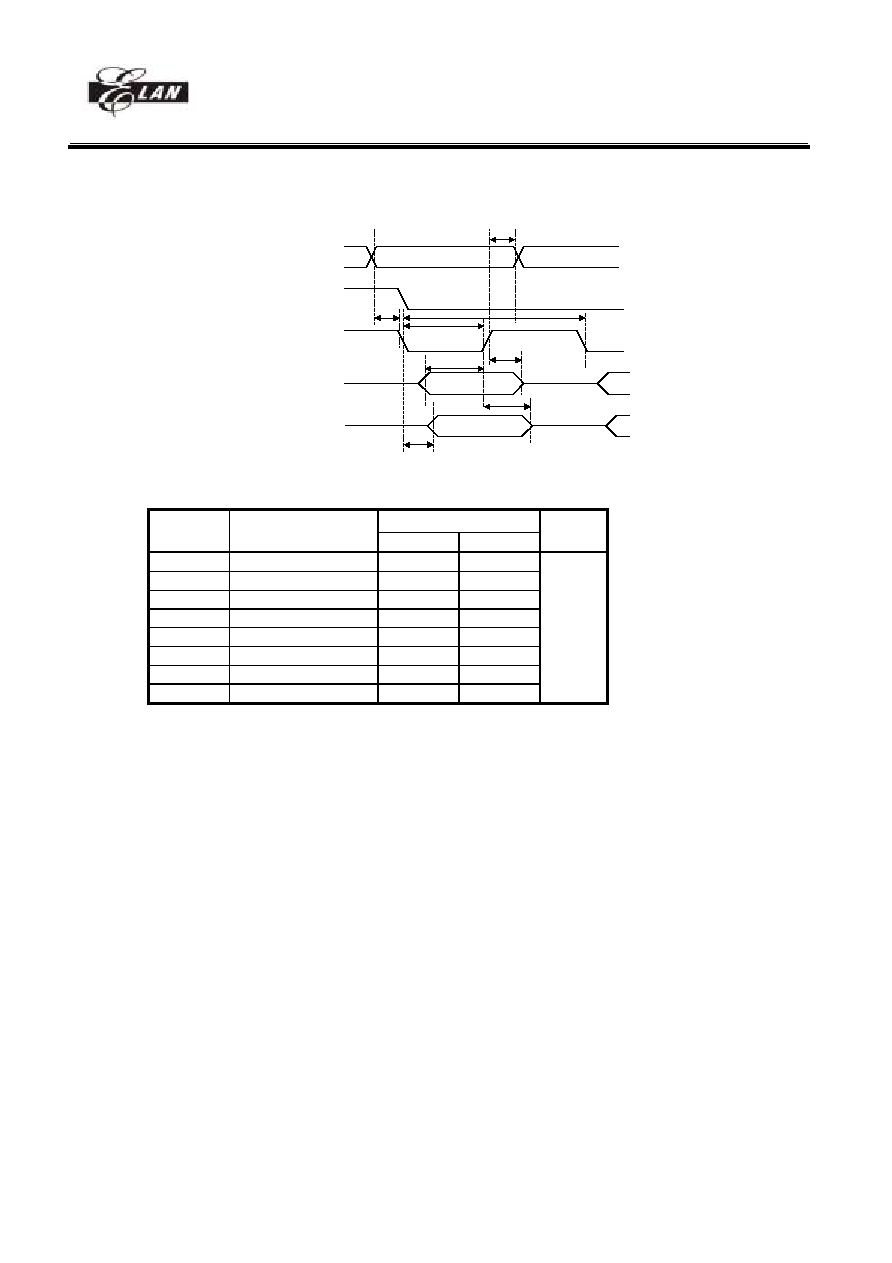
EM78P813
8-bit OTP Micro-controller
__________________________________________________________________________________________________________________________________________________________________
* This specification is subject to change without notice.
46
2004/8/19 (V1.6)
If EXLCD equal to 0, internal LCD driver selected . PortB and PortC output are decided on IOC9 and IOCA Page1.
When EXLCD equal to 1, PortB and PortC are switch to external LCD driver control pin. At this time, when user execute
read or write PORTB instruction, PORTC timing characteristic plot is follow below.
PORTB
DATA
WR(PC2)/
RD(PC3)
CS(PC0/PC1)
A0(PC4)
Taw
Tcyc
Tcc
Tacc
Tds
Tah
Tdh
PORTB
DATA
Toh
Fig.31 timing characteristic of external LCD driver data read/write
Rated value
Symbol Applicable
pins
Min Max
Unit
Tah A0 0
Taw A0 0
Tcyc A0 150
Tcc WR/RD 60
Tds D0
~D7 20
Tdh D0
~D7 10
Tacc D0
~D7 - 60
Toh D0
~D7 10
40
ns
Tah : Address hold time
Taw : Address setup time
Tcyc : System cycle time
Tcc : Pulse width
Tds : Data setup time
Tdh : Data hold time
Tacc : Read access time
Toh : Output disable time
User can operate in coordination on chip Data ROM address automatic increase function to write a large number of
data from internal Data ROM to external LCD RAM.
Example( To collocate EM9L8580 LCD driver ):
START:
MOV A , @0x0C;
IOW IOC5_PAGE0 ;Set Data ROM address automatic increase after read/write data
MOV
A
,
@0x09
IOW IOCB_PAGE1 ;External LCD driver chip 1 INSTRUCTION mode select .
MOV A , @0xB0;
MOV RB_PAGE0 , A ;Set external LCD driver start address PAGE 0
MOV
A
,
@0x10
MOV
RB_PAGE0
,
A
MOV
A
,
@0x00
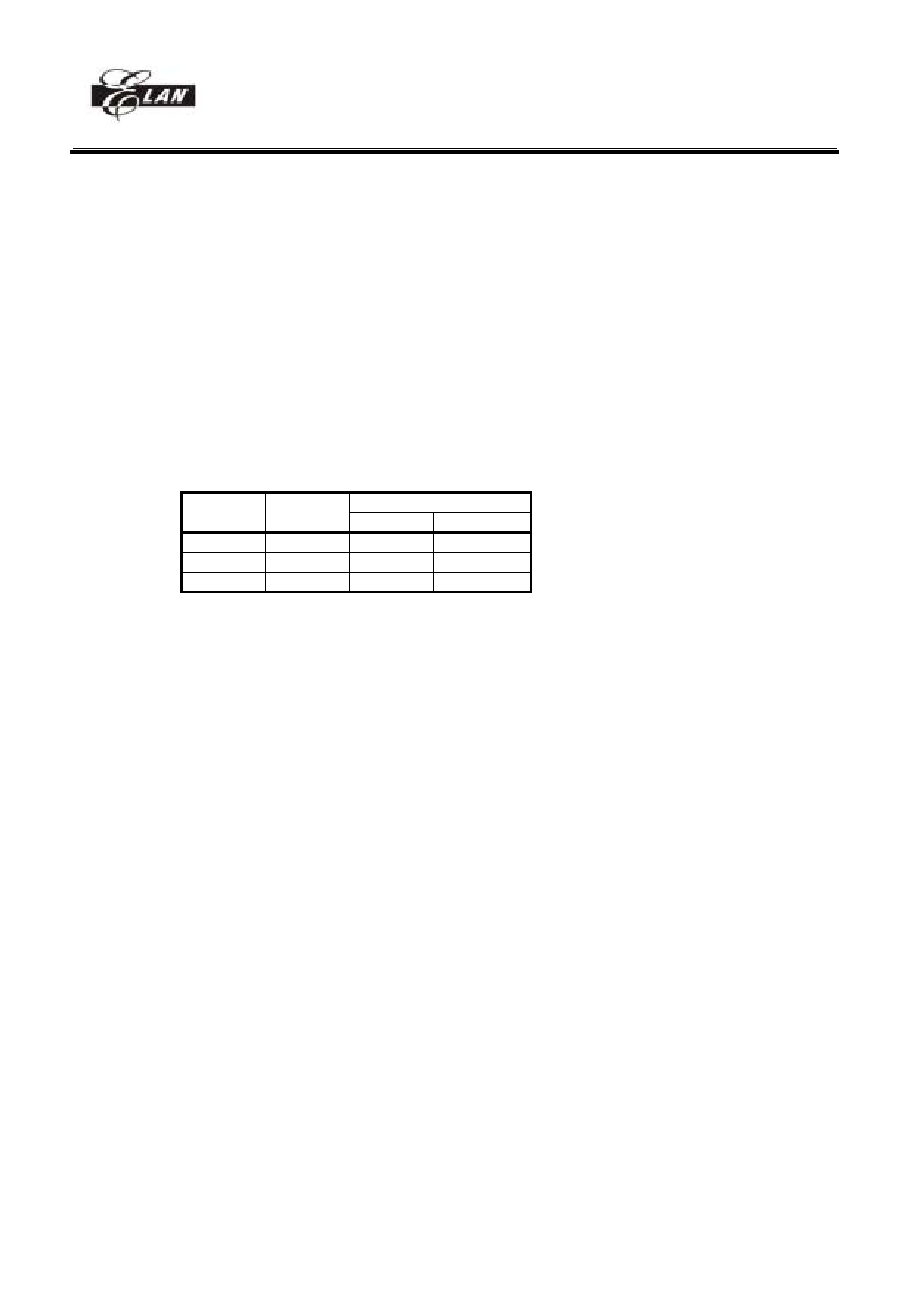
EM78P813
8-bit OTP Micro-controller
__________________________________________________________________________________________________________________________________________________________________
* This specification is subject to change without notice.
47
2004/8/19 (V1.6)
MOV RB_PAGE0 , A ; Set external LCD driver start address Column 0
MOV A , @0x00;
MOV
R7_PAGE1
,
A;
MOV
R8_PAGE1
,
A;
MOV R9_PAGE1 , A ;Start address : 0x00000
MOV A , @0x0B
IOW IOCB_PAGE1 ;select data mode
CN1:
MOV A , R6_PAGE1 ;read data from Data ROM and address flag increase
MOV RB_RAGE0 , A ;write data to external LCD driver.
JMP LOOP
Bit 1(DIS) : External LCD driver DATA/INSTRUCTION switch.
0/1
INSTRACTION/DATA
When EXLCD equal to 1 and DIS bit equal to 0 , MUC will transmit/receive INSTRUCTION. A0(PortC7) will
output 0. If DIS bit set to 1, MUC will transmit/receive DATA. A0(PortC4) will output 1
Bit 2(CSSON) : External LCD driver select enable
CS1..CS2
CSSON CSS0
LOW HIGH
0 X -
CS1,CS2
1 0
CS1
CS2
1 1
CS2
CS1
Example( for EMC 65x132 LCD driver ):
MOV A, @0x01
IOW IOCB_PAGE1
;Select external LCD driver & INSTRUCTURE mode
MOV A,@0xB0
MOV RB,A ;Select external LCD driver COM0
MOV A,@0x10
MOV RB,A
;Select external LCD driver SEG Upper 4-bit = 0
MOV A,@0x00
MOV RB,A
;Select external LCD driver SEG Lower 4-bit = 0
MOV A,@0x03
IOW IOCB_PAGE1
;switch to DATA mode
MOV
A,@0xFF
MOV
RB,A
;write
0xFF to COM0 &SEG0
:
User must assign external LCD address at first time. After writing or reading the display data, The SEGMENT
address is automatically incremented. So that the MUC can continuously write or read data to the address.
Bit 3(CSS) : External LCD driver chip select bit.
0/1 chip1 / chip2
Bit 4..Bit 5(RES0 ~ RES1) : Touch panel bias resister switch..
Bit 6(CWPWR) : CAS decoder power control.
0/1
Power off / Power on.
Bit 7(EXA17) : Expand Data ROM start address MSB. This bit can not set unless CHIPSEL
and EXSEL pin connect to VDD.
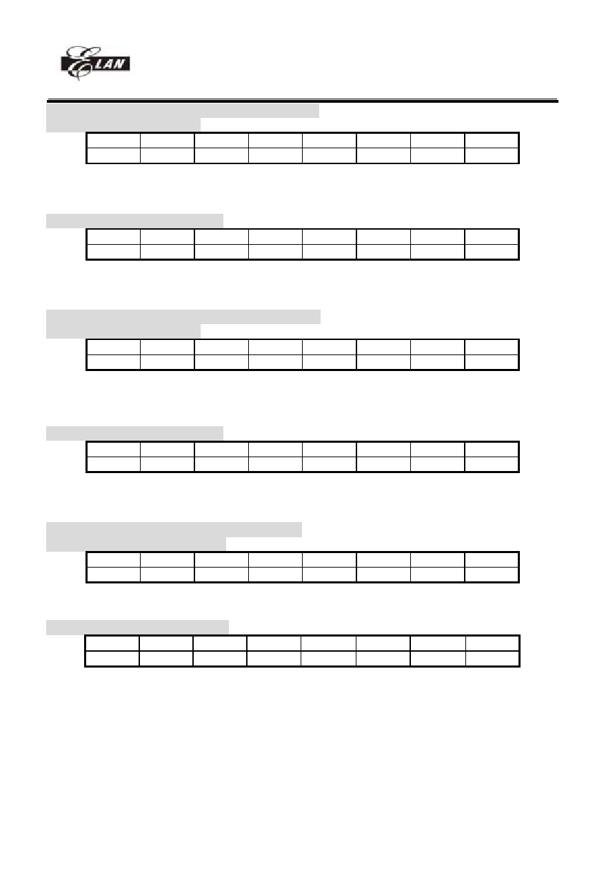
EM78P813
8-bit OTP Micro-controller
__________________________________________________________________________________________________________________________________________________________________
* This specification is subject to change without notice.
48
2004/8/19 (V1.6)
IOCC PORT C I/O Control , Port 6 Pull high register
PAGE0 PORT C I/O Control
7 6 5 4 3 2 1 0
IOCC7 IOCC6
IOCC5 IOCC4
IOCC3
IOCC2
IOCC1 IOCC0
Bit 0~Bit 7 (IOCC0~IOCC7) : PORTC(0~7) I/O direction control register
0 put the relative I/O pin as output
1 put the relative I/O pin into high impedance
PAGE1 Port 6 Pull High Register
7 6 5 4 3 2 1 0
PH67 PH66 PH65 PH64 PH63 PH62 PH61 PH60
Bit 0~Bit 7(PH60~PH67) : PORT6(0~7) pull high control register
0 disable pull high function.
1 enable pull high function
IOCD PORT D I/O Control , Port 7 Pull high register
PAGE0
PORT D I/O Control
7 6 5 4 3 2 1 0
IOCD7 IOCD6
IOCD5 IOCD4
IOCD3
IOCD2
IOCD1 IOCD0
Bit 0~Bit 6 (IOCD0~IOCD6) : PORTD(0~6) I/O direction control register
0 put the relative I/O pin as output
1 put the relative I/O pin into high impedance
PAGE1 Port 7 Pull High Register
7 6 5 4 3 2 1 0
PH77 PH76 PH75 PH74 PH73 PH72 PH71 PH70
Bit 0~Bit 7(PH70~PH77) : PORT7(0~7) pull high control register
0 disable pull high function.
1 enable pull high function
IOCE Interrupt mask , Differential Energy Detect
PAGE0 Interrupt Mask Register1
7 6 5 4 3 2 1 0
INT7 INT6 INT5 INT4 INT3 INT2 INT1 INT0
Bit 0~Bit 7 : Interrupt enable bits.
0/1 disable interrupt/enable interrupt
PAGE1 Differential Energy Detect
7 6 5 4 3 2 1 0
VRSEL DEDD EDGE WUEDD CW_SMB DEDCLK DEDPWR
DEDTHD
Bit 0(DEDTHD) : The minimum detection threshold of Differential Energy Detector (DED)
0/1 -45dBm/-30dBm
Bit 1 (DEDPWR) : Power control of Differential Energy Detector (DED)
0/1 Power off / Power on
Bit 2 (DEDCLK) : Operating clock for Differential Energy Detector (DED)
0/1 32.768kHz/3.5826MHz
This bit is used to select operating clock for Differential Energy Detector (DED). When this bit is set to "1", the
PLL is also enabled regardless of RA bit 6 (ENPLL) . At this time, the Energy detector works at high frequency
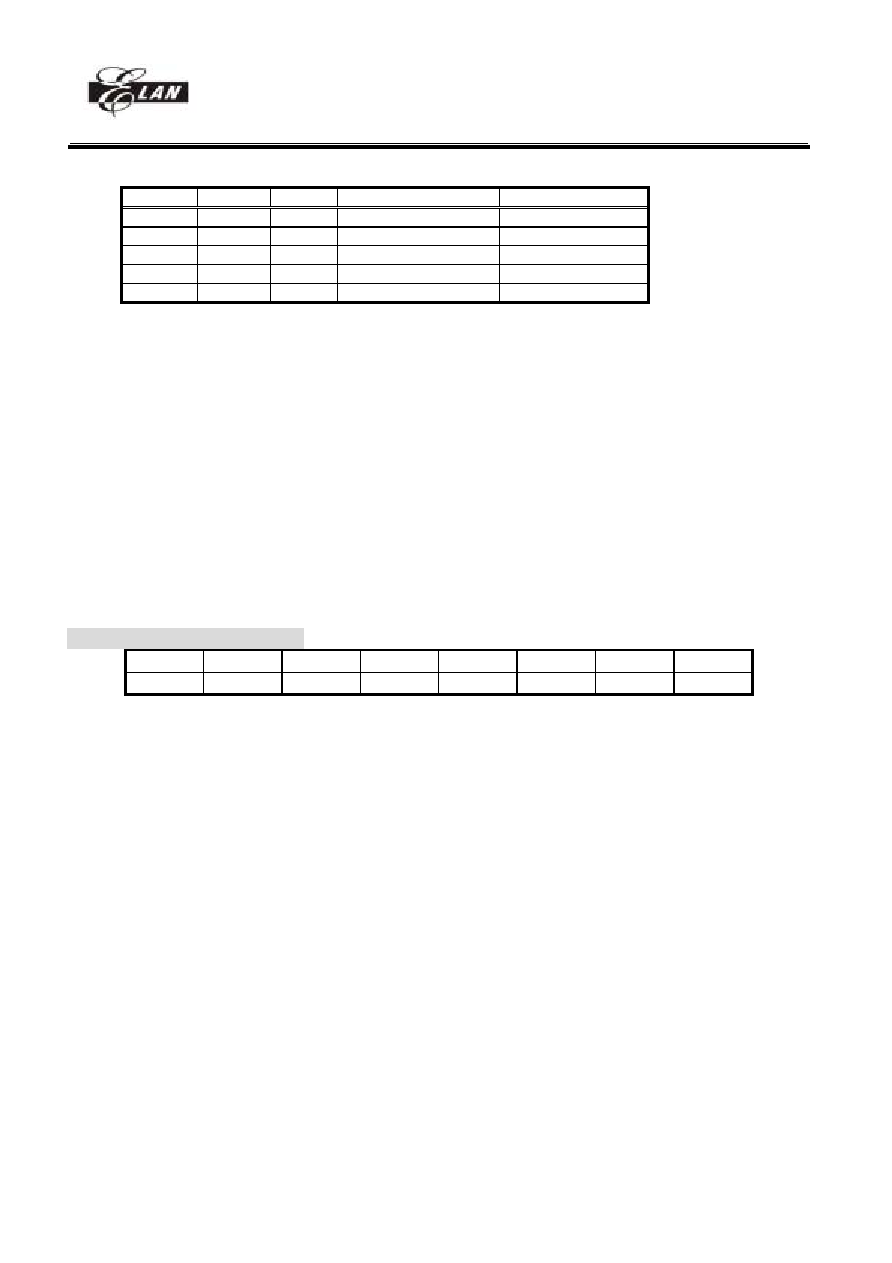
EM78P813
8-bit OTP Micro-controller
__________________________________________________________________________________________________________________________________________________________________
* This specification is subject to change without notice.
49
2004/8/19 (V1.6)
mode. When this bit is set to "0", the Energy Detector works at low frequency mode. The difference between high
frequency and low frequency is as follows.
DEDPWR DEDCLK ENPLL
Energy detector clock
Main CLK
0 X X
X Decision
by
ENPLL
1 0 0 32.768
KHz
Disable
1 0 1 32.768
KHz
Enable
1 1 0 3.5826
MHz
Enable
1 1 1 3.5826
MHz
Enable
PS. "X" means don't care
Bit 3(CW_SMB) : Call Waiting / short message receiver switch
0 Short message mode select.
�
5.5% CAS tone accepted frequency range deviation.(Protocol :
�
5%)
1
Call Waiting mode select. CAS tone accepted frequency range deviation is decided on CODE Option
Register bit 5 ( 1:for Europe and USA / 0:for China )
Bit 4 (WUEDD) : Wake-up control of Energy Detector (DED) output data
1/0 enable/disable
Bit 5 (EDGE) : Wake-up and interrupt trigging edge control of Energy Detector (DED) output
1/0 Falling edge trig. / Rising edge and Falling edge trig.
Bit 6(DEDD) : Output data of Differential Energy Detector (DED) If input signal from TIP/EGIN1 and RING/EGIN2 pin
to Differential Energy Detector is over the threshold level setting at IOCE PAGE 2 bit 0 (DEDTHD), the DED will
extract the zero-crossing pulse waveform corresponding to input signal.
Bit 7 (VRSEL) : Reference voltage VR selection bit for Comparator
0 VR = VDD
1 VR = 2.0V
When this bit is set to "0", V2_0 ref. circuit will be powered off. 2.0V ref. circuit is only powered on when this
bit and RA page2 bit 7(CMPEN) are all set to "1".
IOCF Interrupt Mask Register2
7 6 5 4 3 2 1 0
RBF/STD FSK/CW
0
UART
DED
CNT2
CNT1
TCC
Bit 0~Bit 4, Bit6~Bit7 : Interrupt enable bits.
0/1 disable interrupt/enable interrupt
Bit4: Undefined register. This bit must keep to 0.
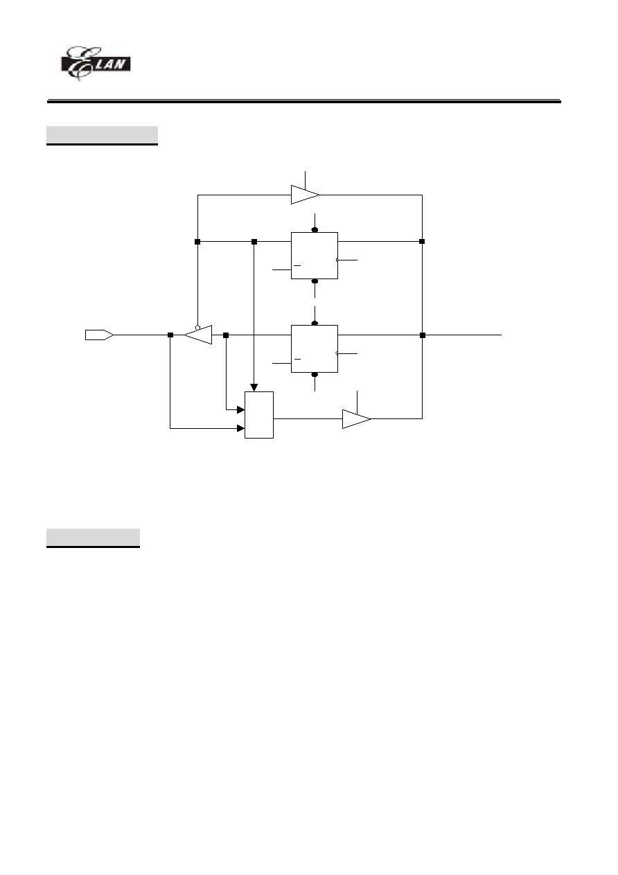
EM78P813
8-bit OTP Micro-controller
__________________________________________________________________________________________________________________________________________________________________
* This specification is subject to change without notice.
50
2004/8/19 (V1.6)
VII.4 I/O PORT
M
U
X
0
1
PDRD
PDWR
CLK
C
L
P
R
D
Q
Q
CLK
C
L
P
R
D
Q
Q
PCWR
IOD
PCRD
PORT
Fig.32 The circuit of I/O port and I/O control register
The I/O registers are bi-directional tri-state I/O ports. The I/O ports can be defined as "input" or "output" pins by the
I/O control registers under program control. The I/O registers and I/O control registers are both readable and writable.
The I/O interface circuit is shown in Fig.27
VII.5 RESET
The RESET can be caused by
(1) Power on voltage detector reset (POVD) and power on reset
(2) WDT timeout. (if enabled and in GREEN or NORMAL mode)
(3) /RESET pin pull low
<Note> At case (1), POVD is controlled by CODE OPTION. If you enable POVD, CPU will reset at 2V under. And
CPU will consume more current about 3uA . And the power on reset is a circuit always enable. It will reset CPU at
about 1.4V and consume about 0.5uA.
Once the RESET occurs, the following functions are performed.
�
The oscillator is running, or will be started.
�
The Program Counter (R2) is set to all "0".
�
When power on, the upper 3 bits of R3 and the upper 2 bits of R4 are cleared.
�
The Watchdog timer and prescaler counter are cleared.
�
The Watchdog timer is disabled.
�
The CONT register is set to all "1"
�
The other register (bit7..bit0)
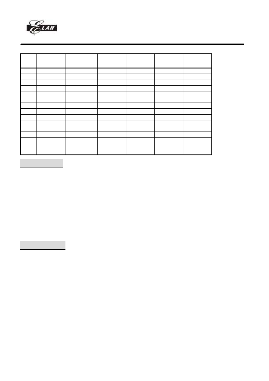
EM78P813
8-bit OTP Micro-controller
__________________________________________________________________________________________________________________________________________________________________
* This specification is subject to change without notice.
51
2004/8/19 (V1.6)
address R register
page0
R register
page1
R register
page2
R register
page3
IOC register
page0
IOC register
page1
1 -- 00000000 00000000 xxxxxxxx
2 --
-- -- --
3 --
-- -- --
4 00xxxxxx xxxxxxxx 10001000 xxx00000
5 x0000000 00000000 00000000 xxxx0000 11110000
xxxxxxxx
6 xxxxxxxx xxxxxxxx 00000000 00000000 11111111 xxxxxxxx
7 xxxxxxxx xxxxxxxx 00000000 00000000 11111111 xxxxxxxx
8 xxxxxxxx xxxxxxxx x0000000 xxxxxxxx 11111111 00000000
9 xxxxxxxx xxxxxxxx 00000xxx
xxxx0000 11111111 00000000
A 00000xx0 xxxxxxxx 00000000 00000000 00000000 00000000
B xxxxxxxx xxxxxxxx 11111111 00000000 11111111 00xx0000
C xxxxxxxx xxxxxxxx 11111111 00000000 11111111 00000000
D xxxxxxxx xxxxxxxx x0011111 xxxxxxxx 11111111 00000000
E 00000000 xxxxxxxx 10000000 xxxxxxxx 00000000 0x000000
F 00000000 xxxxxxxx xxxxxxxx xxxxxxxx 00000000 --
VII.6 wake-up
The controller provided sleep mode for power saving.
SLEEP mode , RA(7)=0 + "SLEP" instruction .
The controller will turn off all the CPU and crystal. Other circuit with power control like key tone control or
PLL control (which has enable register), user has to turn it off by software.
Wake-up from SLEEP mode :
(1) WDT time out
(2) external interrupt
(3) /RESET pull low
All these cases will reset controller , and run the program at address zero. The status just like the power on reset.
Be sure to enable circuit at case (1) or (2).
VII.7 Interrupt
RE and RF is the interrupt status register which records the interrupt request in flag bits. IOCE and IOCF is the
interrupt mask register. TCC timer, Counter1 and Counter2 are internal interrupt source. P70 ~ P77(INT0 ~ INT7) are
external interrupt input which interrupt sources are come from the external. If the interrupts are happened by these
interrupt sources, then RE or RF register will generate '1' flag to corresponding register if you enable IOCE or IOCF
register. Global interrupt is enabled by ENI instruction and is disabled by DISI instruction. When one of the interrupts
(when enabled) generated, will cause the next instruction to be fetched from address 008H. Once in the interrupt
service routine the source of the interrupt can be determined by polling the flag bits in the RE and RF register. The
interrupt flag bit must be cleared in software before leaving the interrupt service routine and enabling interrupts to
avoid recursive interrupts.
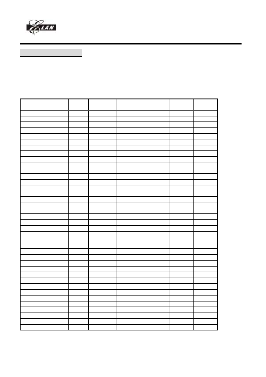
EM78P813
8-bit OTP Micro-controller
__________________________________________________________________________________________________________________________________________________________________
* This specification is subject to change without notice.
52
2004/8/19 (V1.6)
VII.8 Instruction Set
Instruction set has the following features:
(1) Every bit of any register can be set, cleared, or tested directly.
(2) The I/O register can be regarded as general register. That is, the same instruction can operates on I/O register.
The symbol "R" represents a register designator which specifies which one of the 64 registers (including operational
registers and general purpose registers) is to be utilized by the instruction. Bits 6 and 7 in R4 determine the selected
register bank. "b'' represents a bit field designator which selects the number of the bit, located in the register "R'',
affected by the operation. "k'' represents an 8 or 10-bit constant or literal value.
INSTRUCTION
BINARY
HEX MNEMONIC OPERATION
STATUS
AFFECTED
Instruction
cycle
0 0000 0000 0000
0000 NOP
No Operation
None
1
0 0000 0000 0001
0001 DAA
Decimal Adjust A
C
1
0 0000 0000 0010
0002 CONTW
A
CONT
None 1
0 0000 0000 0011
0003 SLEP
0
WDT, Stop oscillator T,P 1
0 0000 0000 0100
0004 WDTC
0
WDT
T,P 1
0 0000 0000 rrrr
000r IOW R
A
IOCR
None 1
0 0000 0001 0000
0010 ENI
Enable Interrupt
None
1
0 0000 0001 0001
0011 DISI
Disable Interrupt
None
1
0 0000 0001 0010
0012 RET
[Top of Stack]
PC
None 2
0 0000 0001 0011
0013 RETI
[Top of Stack]
PC
Enable Interrupt
None 2
0 0000 0001 0100
0014 CONTR
CONT
A
None 1
0 0000 0001 rrrr
001r IOR R
IOCR
A
None 1
0 0000 0010 0000
0020 TBL
R2+A
R2 bits
9,10 do not clear
Z,C,DC 2
0 0000 01rr rrrr
00rr MOV R,A
A
R
None 1
0 0000 1000 0000
0080 CLRA
0
A
Z 1
0 0000 11rr rrrr
00rr CLR R
0
R
Z 1
0 0001 00rr rrrr
01rr SUB A,R
R-A
A
Z,C,DC 1
0 0001 01rr rrrr
01rr SUB R,A
R-A
R
Z,C,DC 1
0 0001 10rr rrrr
01rr DECA R
R-1
A
Z 1
0 0001 11rr rrrr
01rr DEC R
R-1
R
Z 1
0 0010 00rr rrrr
02rr OR A,R
A
R A
Z 1
0 0010 01rr rrrr
02rr OR R,A
A
R R
Z 1
0 0010 10rr rrrr
02rr AND A,R
A & R
A
Z 1
0 0010 11rr rrrr
02rr AND R,A
A & R
R
Z 1
0 0011 00rr rrrr
03rr XOR A,R
A
R A
Z 1
0 0011 01rr rrrr
03rr XOR R,A
A
R R
Z 1
0 0011 10rr rrrr
03rr ADD A,R
A + R
A
Z,C,DC 1
0 0011 11rr rrrr
03rr ADD R,A
A + R
R
Z,C,DC 1
0 0100 00rr rrrr
04rr MOV A,R
R
A
Z 1
0 0100 01rr rrrr
04rr MOV R,R
R
R
Z 1
0 0100 10rr rrrr
04rr COMA R
/R
A
Z 1
0 0100 11rr rrrr
04rr COM R
/R
R
Z 1
0 0101 00rr rrrr
05rr INCA R
R+1
A
Z 1
0 0101 01rr rrrr
05rr INC R
R+1
R
Z 1
0 0101 10rr rrrr
05rr DJZA R
R-1
A, skip if zero
None
2 if skip
0 0101 11rr rrrr
05rr DJZ R
R-1
R, skip if zero
None
2 if skip
EM78P813
8-bit OTP Micro-controller
__________________________________________________________________________________________________________________________________________________________________
* This specification is subject to change without notice.
53
2004/8/19 (V1.6)
0 0110 00rr rrrr
06rr RRCA R
R(n)
A(n-1)
R(0)
C, C A(7)
C 1
0 0110 01rr rrrr
06rr RRC R
R(n)
R(n-1)
R(0)
C, C R(7)
C 1
0 0110 10rr rrrr
06rr RLCA R
R(n)
A(n+1)
R(7)
C, C A(0)
C 1
0 0110 11rr rrrr
06rr RLC R
R(n)
R(n+1)
R(7)
C, C R(0)
C 1
0 0111 00rr rrrr
07rr SWAPA R
R(0-3)
A(4-7)
R(4-7)
A(0-3)
None 1
0 0111 01rr rrrr
07rr SWAP R
R(0-3)
R(4-7)
None 1
0 0111 10rr rrrr
07rr JZA R
R+1
A, skip if zero
None
2 if skip
0 0111 11rr rrrr
07rr JZ R
R+1
R, skip if zero
None
2 if skip
0 100b bbrr rrrr
0xxx BC R,b
0
R(b)
None 1
0 101b bbrr rrrr
0xxx BS R,b
1
R(b)
None 1
0 110b bbrr rrrr
0xxx JBC R,b
if R(b)=0, skip
None
2 if skip
0 111b bbrr rrrr
0xxx JBS R,b
if R(b)=1, skip
None
2 if skip
1 00kk kkkk kkkk
1kkk CALL k
PC+1
[SP]
(Page, k)
PC
None 2
1 01kk kkkk kkkk
1kkk JMP k
(Page, k)
PC
None 2
1 1000 kkkk kkkk
18kk MOV A,k
k
A
None 1
1 1001 kkkk kkkk
19kk OR A,k
A
k A
Z 1
1 1010 kkkk kkkk 1Akk AND A,k
A & k
A
Z 1
1 1011 kkkk kkkk 1Bkk XOR A,k
A
k A
Z 1
1 1100 kkkk kkkk 1Ckk RETL k
k
A, [Top of Stack]
PC
None 2
1 1101 kkkk kkkk 1Dkk SUB A,k
k-A
A
Z,C,DC 1
1 1110 0000 0001
1E01 INT
PC+1
[SP]
001H
PC
None 1
1 1110 1kkk kkkk
1E8k PAGE k
K->R5(4:0)
None
1
1 1111 kkkk kkkk
1Fkk ADD A,k
k+A
A
Z,C,DC 1
** 1 Instruction cycle = 2 main CLK
EM78P813
8-bit OTP Micro-controller
__________________________________________________________________________________________________________________________________________________________________
* This specification is subject to change without notice.
54
2004/8/19 (V1.6)
VII.9 CODE Option Register
The controller has one CODE option register which is not part of the normal program memory. The option bits cannot be
accessed during normal program execution.
CODE Option Register1 ( Program ROM)
7 6 5 4 3 2 1 0
-
CWMODE
/DED
/PTB
Bit 0(/PTB) : Program ROM data protect bit.
0/1 protect / unprotect
When user clear this bit to 0, another person will unable read the originally program code from program ROM.
Bit 1(/DED) : enable/disable DED function.
0 enable DED function
1 disable DED function
Bit 2(CWMODE) : CAS tone (2130 Hz plus 2750 Hz ) accepted frequency range select.
0
�
2% Call waiting accepted frequency range deviation.(Application for China protocol :
�
1.5% )
1
�
1.2% Call waiting accepted frequency range deviation.(Application for Europe and USA protocol :
�
0.5% )
CODE Option Register2 ( Data ROM)
7 6 5 4 3 2 1 0
0 0 0 0 0 0 0
/DTB
Bit 0(PTB) : Data ROM data protect bit.
0/1 protect / unprotect
When user clear this bit to 0, another person will unable read the originally program code from data ROM.
Bit 1~Bit 7 : Unused
PAD Option
/POVD(power on voltage detect) reset can be enabled/disabled by PAD Option. This POVD pad is not shown on the pin
assignment. Internally or externally connecting this pad to GND/VDD to enable/disable /POVD reset.
/POVD
2.2V /POVD reset voltage
2.2V Power on reset voltage
Sleep mode current (VDD=5V)
1 No
Yes
(2.2V)
1uA
0 Yes
(2.2V)
No
15uA
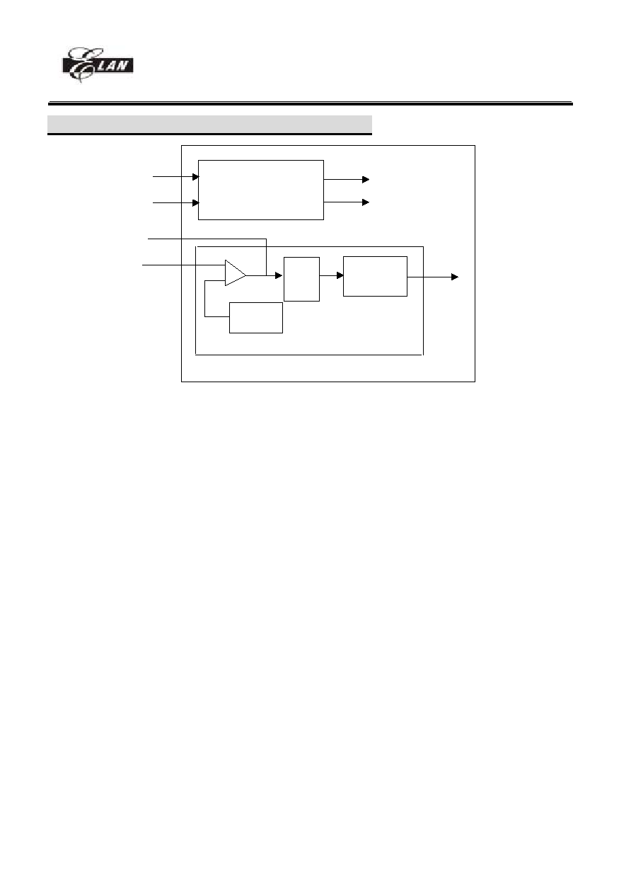
EM78P813
8-bit OTP Micro-controller
__________________________________________________________________________________________________________________________________________________________________
* This specification is subject to change without notice.
55
2004/8/19 (V1.6)
VII.10 CALL WAITING Function Description
CWTIP
Filter
Vdd/2
Detection
block
Voltage
reference
GAIN
FSK
demodulator
TIP
RING
-
+
CAS
DATA
/CD
Fig.33 Call Waiting Block Diagram
Call Waiting service works by alerting a customer engaged in a telephone call to a new incoming call. This way
the customer can still receive important calls while engaged in a current call. The CALL WAITING DECODER can
detect CAS(Call-Waiting Alerting Signal 2130Hz plus 2750Hz) and generate a valid signal on the data pins.
The call waiting decoder is designed to support the Caller Number Deliver feature, which is offered by regional
Bell Operating Companies.
In a typical application, after enabling CW circuit (by R5 page3 bit3 & bit4 ) this IC receives Tip and Ring
signals from twisted pairs. The signals as inputs of pre-amplifier, and the amplifier sends input signal to a band pass
filter. Once the signal is filtered, the Detection block decodes the information and sends it to RE page2 bit7 . The
output data made available at RE CAS bit.
The data is CAS signals. The CAS is normal high. When this IC detects 2130Hz and 2750Hz frequency, then
CAS pin goes to low.
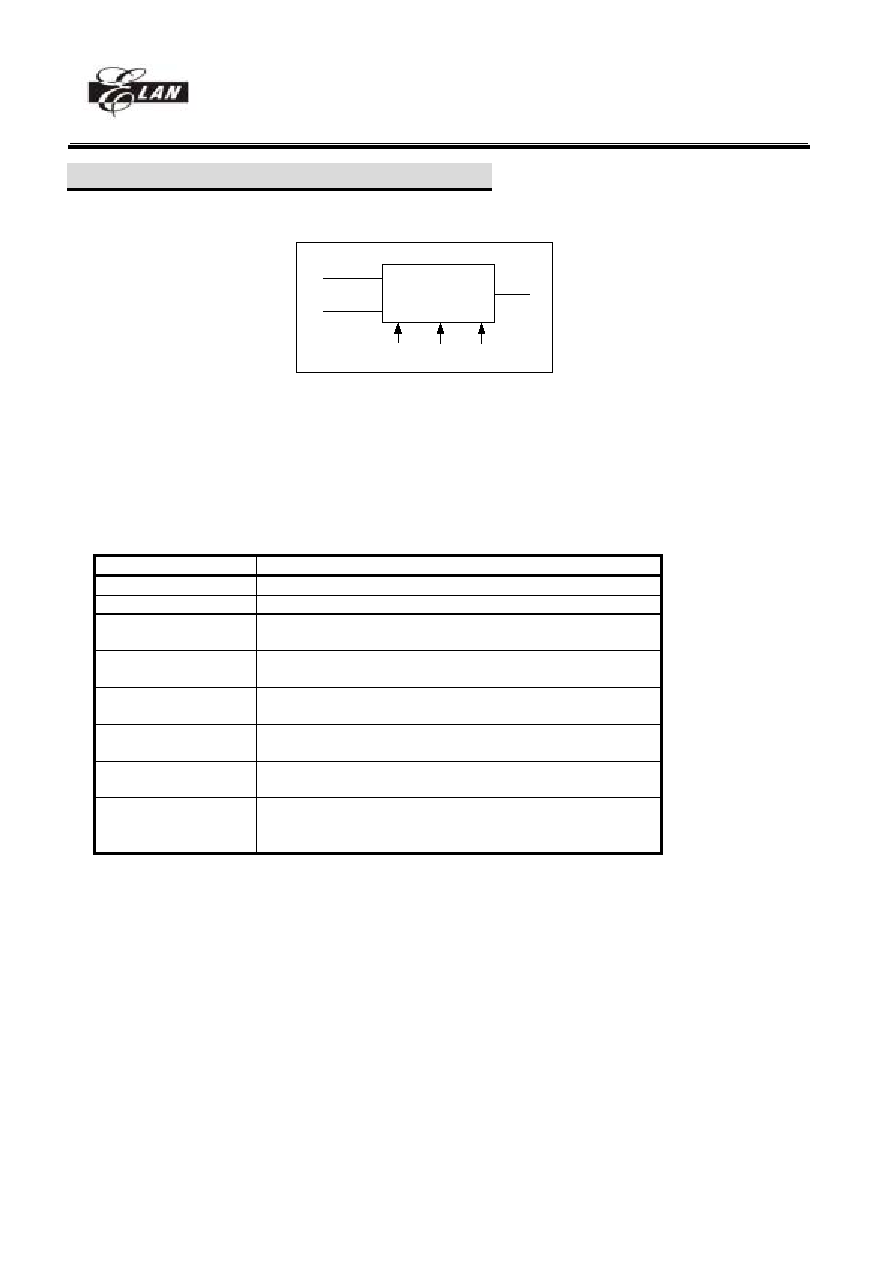
EM78P813
8-bit OTP Micro-controller
__________________________________________________________________________________________________________________________________________________________________
* This specification is subject to change without notice.
56
2004/8/19 (V1.6)
VII.11 Differential Energy Detector (DED)
DED
DEDD
EGIN1
DEDTHD
DEDPWR
EGCLK
EGIN2
Fig.34 DED Block diagram
The Differential Energy Detector is differential input level and zero crossing detector named as DED. It can
detect any incoming AC signal above its threshold level and output corresponding zero-crossing frequency pulse. For
this energy detector, the user can set it's minimum detection threshold level at �35dBm or �45dBm by DEDTHD bit.
All the minimum detection value can be achieved under input capacitor more than 4700pF and input resistor around
100k ohms. The energy detector has power control by IOCE PAGE1 bit 1 (DEDPWR).
Register bits of Energy Detector :
Register bits
Descriptions
RE PAGE0 bit 3 (DED) DED : Interrupt flag of DED output data
RE PAGE1 bit 7 (DEDD) DEDD : Output data of DED
IOCE PAGE1
Bit 5 (EDGE)
EDGE : edge control of DED output data
1/0 => Falling edge trig. / Rising edge and Falling edge trig.
IOCE PAGE1
Bit 4 (WUEDD)
WUEDD : Wake-up control of DED output data
1/0 => enable/disable
IOCE PAGE1
Bit 6 (DED)
DED : Interrupt mask of DED output data
1/0 enable/disable interrupt of DED output data
IOCE PAGE1
Bit 0 (DEDTHD)
DEDTHD : Minimum detection threshold of DED
0/1 -45dBm/-35dBm
IOCE PAGE1
Bit 1 (DEDPWR)
DEDPWR : Power control of DED
0/1 power off/power on
IOCE PAGE1
Bit 2 (DEDCLK)
DEDCLK : operating clock of DED
0 : low frequency clock
1 : high frequency clock
EM78P813
8-bit OTP Micro-controller
__________________________________________________________________________________________________________________________________________________________________
* This specification is subject to change without notice.
57
2004/8/19 (V1.6)
VIII. Absolute Operation Maximum Ratings
RATING SYMBOL
Min
Typ
Max
Unit
DC SUPPLY VOLTAGE
VDD
-0.3
6
V
INPUT VOLTAGE
Vin
VDD-0.5
VDD
VDD+0.5
V
OPERATING TEMPERATURE RANGE
Ta
0
25
70
IX. DC Electrical Characteristic
(Operation current consumption for Analog circuit)
Parameter Symbol
Condition Min Typ
Max
Unit
Operation current for FSK
I_FSK
VDD=5V, CID power on
2.5
4 mA
VDD=3V, CID power on
2.0
3.5
Operation current for CW
I_CW
VDD=5V, CID power on
2.5
4 mA
VDD=5V, CID power on
2.0
3.5
Operation current for DTMF I_DR
VDD=3V, DTMFr power on
2.5
4.0 mA
Receiver
VDD=3V,
DTMFr power on
2.0
3.5
Operation current for TONE I_DTMF
VDD=5V, DTMF power on
0.9
1.2 mA
generator
VDD=3V, DTMF power on
0.5
0.8
Current DA output current
I_DA
VDD=5V, CDA power on
2.5
4 mA
VDD=3V, CDA power on
2.0
3.5
Operation current for OP
I_OP
VDD=5V, PT power on
0.17
mA
VDD=3V, PT power on
0.1
Operation current for
I_CMP
VDD=5V, PT power on
0.15
0.3 mA
Comparator
VDD=3V, PT power on
0.13
0.2
(Ta=25
�C, VDD=5V�5%, VSS=0V)
Parameter Symbol
Condition Min Typ
Max
Unit
Input Leakage Current for
input pins
IIL1
VIN = VDD, VSS
�1
�A
Input Leakage Current for
bi-directional pins
IIL2
VIN = VDD, VSS
�1
�A
Input High Voltage
VIH
2.0
V
Input
Low
Voltage
VIL
0.8
V
Input high threshold Voltage VIHT
/RESET, TCC, RDET1
2.0
V
Input low threshold Voltage VILT
/RESET, TCC,RDET1
0.8
V
Clock Input High Voltage
VIHX
OSCI
1.8
V
Clock Input Low Voltage
VILX
OSCI
1.2
V
Output High Voltage
(port 8,9,B,C,D)
VOH1
IOH
=
-6mA
2.0 2.4
V
(port6,7,D)
IOH
=
-10.0mA
2.0 2.4
V
Output Low Voltage
(port 8,9,B,C,D)
VOL1 IOL
=
6mA
0.4
V
(port6,7)
IOL
=
10.0mA
0.4
V
Pull-high current
IPH
Pull-high active input pin at
VSS
-10
-15
�A
Power down current
(SLEEP mode)
ISB1
All input and I/O pin at
VDD, output pin floating,
1 4
�A
EM78P813
8-bit OTP Micro-controller
__________________________________________________________________________________________________________________________________________________________________
* This specification is subject to change without notice.
58
2004/8/19 (V1.6)
WDT disabled
Low clock current
(GREEN mode)
ISB2 CLK=32.768KHz,All
analog
circuit disable , All input and
I/O pin at VDD, output pin
floating, WDT disabled,
LCD disable
35
50
�A
Operating supply current
(NORMAL mode)
ICC
/RESET=High, PLL enable
CLK=3.579MHz, output pin
floating, LCD disable, all
analog circuit disable
2.8 3.5 mA
Tone generator reference
voltage
Vref2
0.5
0.7 VDD
Differential Energy Detector (DED) (Ta=25
�C, VDD=5.0V�5%, VSS=0V)
Symbol Parameter
Condition
Min Typ
Max
Unit
EGIN1
Operating current for SED
SEDCLK bit = 0
20
25
A
�
EGIN2
Operating current for SED
SEDCLK bit = 0
20
25
A
�
Embedded LCD driver
Symbol Parameter
Condition
Min Typ
Max
Unit
Ron
LCD driver ON resistance
LCD function enable
2
4
k
1/24
duty
88
Hz
FM
f
LCD frame frequency
1/16 , 1/32 duty
64
Hz
DCC
I
Dynamic current consumption Charge pump x 2 , no load
60
65
A
�
OUT
V
Voltage converter output
Charge pump x 2 , no load
95
97
%
Weak mode
75
A
�
Normal mode
150
A
�
Strong mode
300
A
�
driver
I
LCD driver current
Double strong mode
600
A
�
X. AC Electrical Characteristic
CPU instruction timing (Ta=25
�C, VDD=5V, VSS=0V)
Parameter Symbol
Condition
Min
Typ
Max
Unit
Input CLK duty cycle
Dclk
45
50
55
%
Instruction cycle time
Tins
32.768kHz
3.579MHz
60
550
us
ns
Device delay hold time
Tdrh
16
ms
TCC
input
period Ttcc Note
1 (Tins+20)/N
ns
Watchdog timer period
Twdt
Ta = 25
�C
16
ms
Note 1: N= selected prescaler ratio.
EM78P813
8-bit OTP Micro-controller
__________________________________________________________________________________________________________________________________________________________________
* This specification is subject to change without notice.
59
2004/8/19 (V1.6)
FSK AC Characteristic (Vdd=5V,Ta=+25
�C)
CHARACTERISTIC Min
Typ
Max Unit
FSK sensitivity
Low Level Sensitivity Tip & Ring @SNR 20dB
-40
-48
dBm
High Level Sensitivity Tip & Ring @SNR 20dB
0
dBm
Signal Reject
-51
dBm
FSK twist
Positive
Twist
(High
Level)
+10
dB
Positive Twist (Low Level)
+10
dB
Negative Twist (High Level)
-6
dB
Negative Twist (Low Level)
-6
dB
DTMF (DTMF receiver) AC Characteristic (Vdd=5V,Ta=+25
�C)
CHARACTERISTIC Min
Typ
Max Unit
DTMF receiver
Low Level Signal Sensitivity
-36
dBm
High Level Signal Sensitivity
0
dBm
Low Tone Frequency
�2
%
High Tone Frequency
�2
%
DTMF receiver noise endurance
Signal to noise ratio
15
dB
TONE generators for AC Characteristic (Vdd=5V,Ta=+25
�C)
CHARACTERISTIC Min
Typ
Max Unit
Tone1/Tone2 signal strength (root mean square voltage)
Tone1 signal strength V1rms (ps1)
130
155 180 V
Tone2 signal strength V2rms (ps1)
1.259V1rms
V
Tone twist
(Tone1 � Tone2) twist
-2
dB
Tone frequency deviation
Frequency deviation
�1
%
(ps1) : V1rms and V2rms has 2dB difference. It means 20log(V2rms/V1rms) = 20log1.259 = 2 (dB)
DED AC Characteristic (Vdd=+5.0V,Ta=+25)
CHARACTERISTIC MIN
TYP
MAX
UNIT
Input sensitivity TIP and RING for DED, DEDTHD bit=0
-45
--
dBm
Input sensitivity TIP and RING for DED, DEDTHD bit=1
-35
--
dBm
Timing characteristic (Vdd=5V,Ta=+25
�C)
Description Symbol
Min Typ
Max Unit
Oscillator timing characteristic
OSC start up
32.768kHz
Tosc
1500 ms
3.579MHz
PLL
5
10
us
FSK timing characteristic
Carrier
detect
low
Tcdl
-- 10 14 ms
Carrier detect low to data valid
Tcdv
--
10
20
ns
Power up to FSK(setup time)
Tsup
--
15
20
ms
End of FSK to Carrier Detect high
Tcdh
--
4
ms
EM78P813
8-bit OTP Micro-controller
__________________________________________________________________________________________________________________________________________________________________
* This specification is subject to change without notice.
60
2004/8/19 (V1.6)
CW timing characteristic
CAS input signal length
(2130 ,2750 Hz @ -20dBm )
Tcasi 80
ms
Call waiting data detect delay time
Tcwd
42
ms
Call waiting data release time
Tcwr
26
ms
DTMF receiver timing characteristic
Tone Present Detection Time
Tdp
(ps1)
the guard-times for tone-present
(C=0.1uF, R=300K)
Tgtp 30
ms
the guard-times for tone-absent
(C=0.1uF, R=300K)
Tgta 30
mS
Propagation Delay (St to Q)
Tpq
8
us
Tone
Absent
Detection
Time
Tda (ps2) ms
SPI timing characteristic (CPU clock 3.58MHz and Fsco = 3.58Mhz /2)
/SS set-up time
Tcss
560
ns
/SS hold time
Tcsh
250
SCLK
high
time
Thi
250
ns
SCLK low time
Tlo
250
ns
SCLK
rising
time
Tr
15 30 ns
SCLK
falling
time
Tf
15 30 ns
SDI set-up time to the reading edge of SCLK
Tisu
25
ns
SDI hold time to the reading edge of SCLK
Tihd
25
ns
SDO
disable
time
Tdis 560
ns
(ps1) : Controlled by software
(ps2) : Controlled by RC circuit.
Data ROM access timing characteristic
Symbol Description
Condition Min Typ
Max
Unit
Tdiea
Delay from Phase 3 end to
INSEND active
Cl=100pF
30
ns
Tdiei
Delay from Phase 4 end to
INSEND inactive
Cl=100pF
30
ns
Tiew INSEND
pulse
width
30 ns
Tdca
Delay from Phase 4 end to
CA Bus valid
C1=100pF
30
ns
Tacc
ROM data access time
100
ns
Tcds
ROM data setup time
20
ns
Tcdh
ROM data hold time
20
ns
Tdca-1
Delay time of CA-1
C1=100pF
30
ns

EM78P813
8-bit OTP Micro-controller
__________________________________________________________________________________________________________________________________________________________________
* This specification is subject to change without notice.
61
2004/8/19 (V1.6)
XI. Timing Diagrams
ins
Fig.38 AC timing
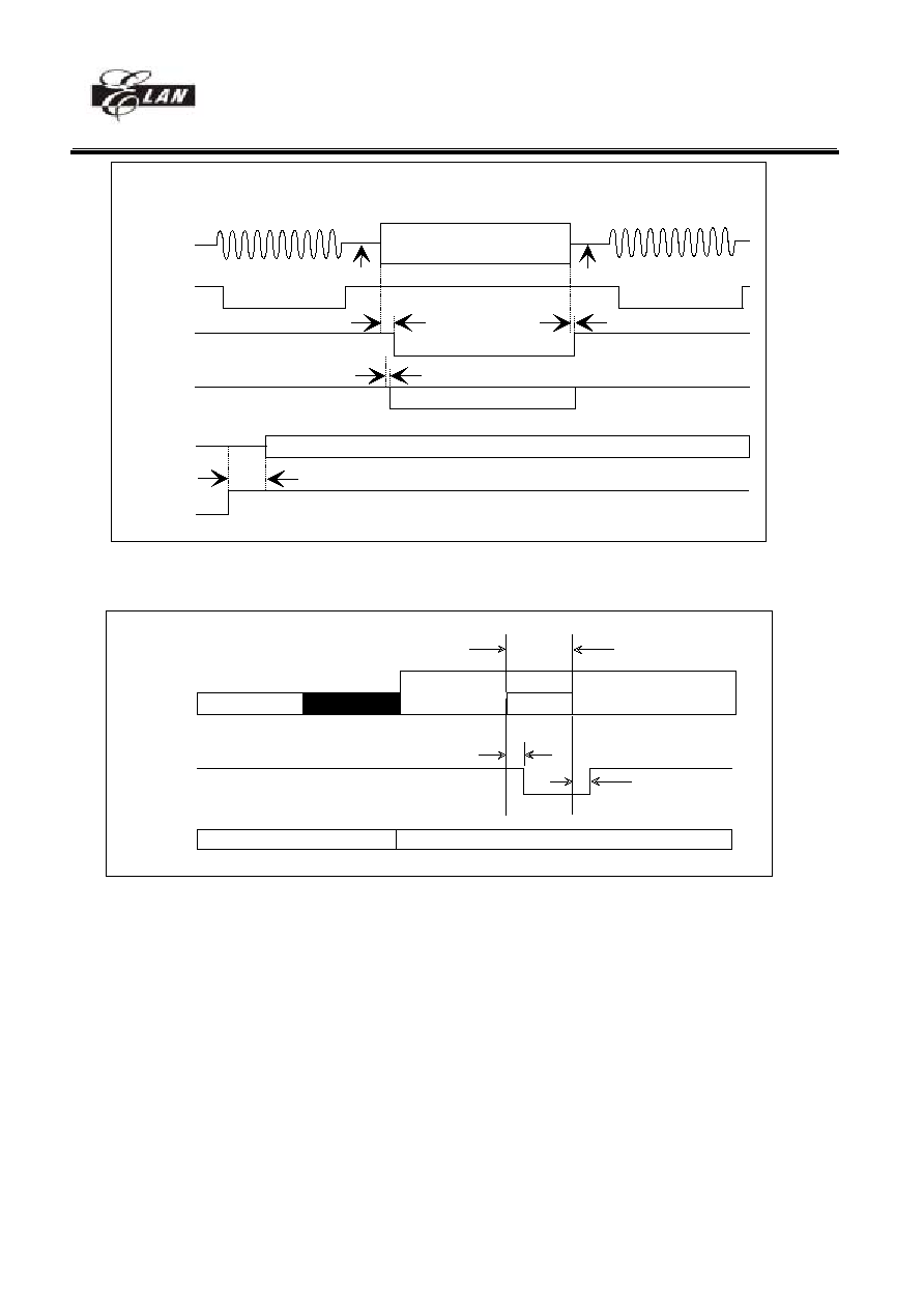
EM78P813
8-bit OTP Micro-controller
__________________________________________________________________________________________________________________________________________________________________
* This specification is subject to change without notice.
62
2004/8/19 (V1.6)
TIP/RING
/ TRIG
/CD
DATA
(internal
clock)
FIRST RING
2 SECONDS
0.5 SEC
0.5 SEC
SECOND RING
2SECONDS
3.579 M Hz
Tcdl
/358E
Tdoc
Tsup
Tcdh
DATA
Fig.39 FSK timing diagram
CWPWR
power off
power on
events
Tc w d
p lu g in
o n
h o o k
in use
CAS
Tc a s i
CAS
Tc w r
normal
Fig.40 Call waiting timing diagram
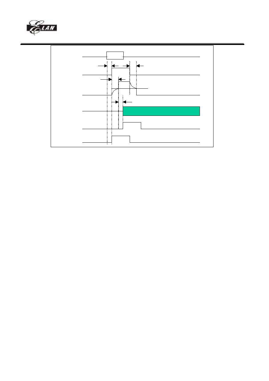
EM78P813
8-bit OTP Micro-controller
__________________________________________________________________________________________________________________________________________________________________
* This specification is subject to change without notice.
63
2004/8/19 (V1.6)
TONE
TONE
EST
ST/GT
Vtst
1/2 VDD
Q4..Q1
STD
LINE_ENG
Tdp
5~20mS
by S/W
Tgta
30mS Typ.
Tgtp
30mS Typ.
Tpq
8 uS Typ.
Fig.41 DTMF receiver timing diagram
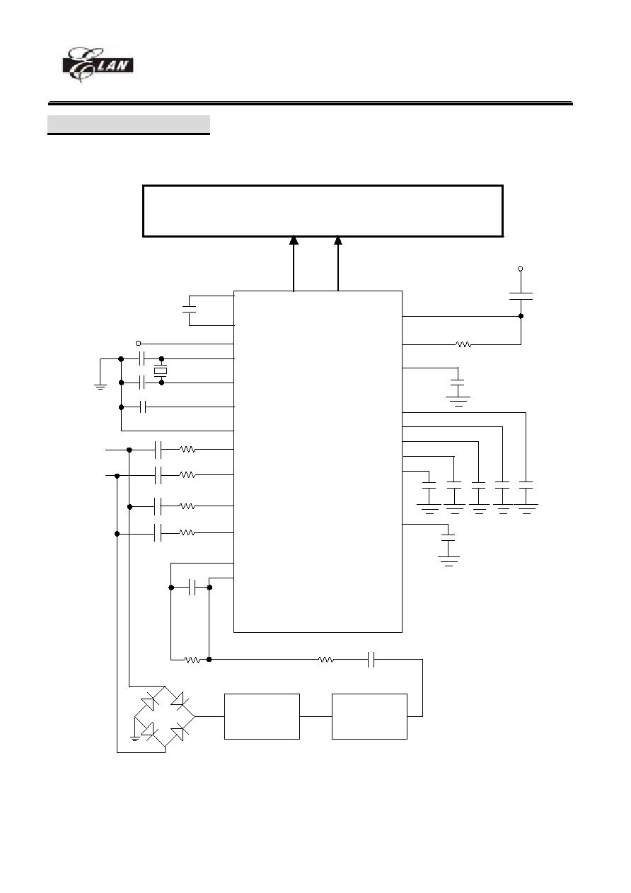
EM78P813
8-bit OTP Micro-controller
__________________________________________________________________________________________________________________________________________________________________
* This specification is subject to change without notice.
64
2004/8/19 (V1.6)
XII Application Circuit
LCD pannel
VDD
XIN
XOUT
0.1u
PLLC
SEGMENT
32.768k
27p
27p
AVSS,GND
EM78P813
TIP
RING
4700p
47K
VDD
STGT
EST
4700p
47K
Line
Interface
Speech
Network
39K
4700p
CWIN
CWGS
47p
150K
TIP
RING
LINE
VDD,AVDD,LVDD
COMMON
32x98 pixels
4.7u
CA
CB
VOUT
1u
VC5
1u
VC4
VC3
1u
VC1
VC2
1u
1u
1u
VREF
1u
EGIN1
4700p
47K
EGIN1
4700p
47K
Fig.43 Internal LCD driver application circuit
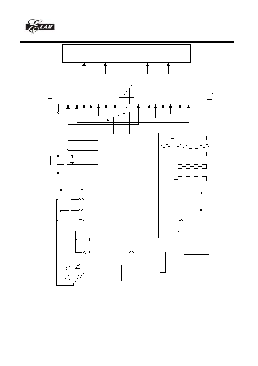
EM78P813
8-bit OTP Micro-controller
__________________________________________________________________________________________________________________________________________________________________
* This specification is subject to change without notice.
65
2004/8/19 (V1.6)
LCD pannel
P70
SEG50
SEG51
SEG52
SEG65
VDD
XIN
XOUT
0.1u
PLLC
COMMON
SEGMENT
32.768k
27p
27p
AVSS,GND
EM78P813
TIP
RING
4700p
47K
Key matrix
LCD driver
EM9L8580(master)
D0..D7
PB7~PB0
8
CLK A0 /RD /WR /CS1
4700p
47K
Line
Interface
Speech
Network
39K
4700p
CWIN
CWGS
47p
150K
TIP
RING
LINE
( support max 65x132 pixels)
VDD,AVDD
P71
P72
P73
LCD driver
EM9L8580(slave)
D0..D7 CLK A0 /RD /WR /CS1
( support max 65x132 pixels)
SEGMENT
COMMON
FR
FR
CL
CL
/DOF
/DOF
V0
V1
V2
V3
V4
V0
V1
V2
V3
V4
65x264 pixels
M/S
M/S
VDD
PC
4
PC
5
PC
6
PC
7
/RES
/RES
PC
3
P/S
P/S
VDD
XOU
T
Re
s
e
t
TIP
RING
4700p
47K
4700p
47K
VDD
STGT
EST
EXTERNAL
Memory
SEG34 ~ SEG65
(Share with interface)
Fig.44 External multi-chip LCD driver application circuit