
EM78P915
8-BIT MICRO-CONTROLLER
Product
specification v2.0
ELAN MICROELECTRONICS CORP.
No. 12, Innovation 1
st
RD., Science-Based Industrial Park
Hsin Chu City, Taiwan
TEL: (03) 5639977
FAX: (03) 5630118
EM78P915
8-bit Micro-controller
__________________________________________________________________________________________________________________________________________________________________
* This specification is subject to be changed without notice.
2005/12/21 (V2.0)
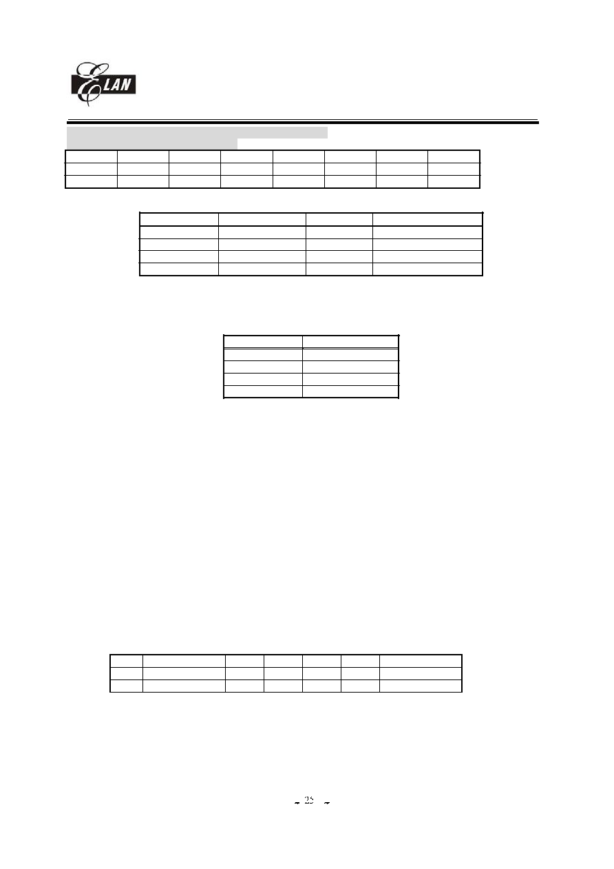
Version History
Specification revision history for EM78P915
Version
Description
1.1
Add program pin location table
1.2
Pin assignment change, and POR=2.0V, green mode=2.2~5.5V
Oscillator start to stable time will smaller/equal 0.5 sec, remove LCD driving
Ability control
1.3
Add SDT characteristic table
R4 page bit7 (RBF) is modified to Read-only
"End of FSK to carrier detect high" is 5 ms
Update table 24
Modify R7, IOC7, IOCB, value in table 1
1.4
Add interrupt node, note7 and note8 in page3
1.5
Bug modify in page 21
1.6
Add notice about setting code-option and /POVD on/off in page 3.
1.7
Remove DED function, operation voltage = 3.1V at 10.74MHz
1.8
Modify TDP1/2 description in page 34
1.9
Add chip pad diagram, modify /POVD description
2.0
Add P915/915 family list and development tool list in appendix C, D, E, F
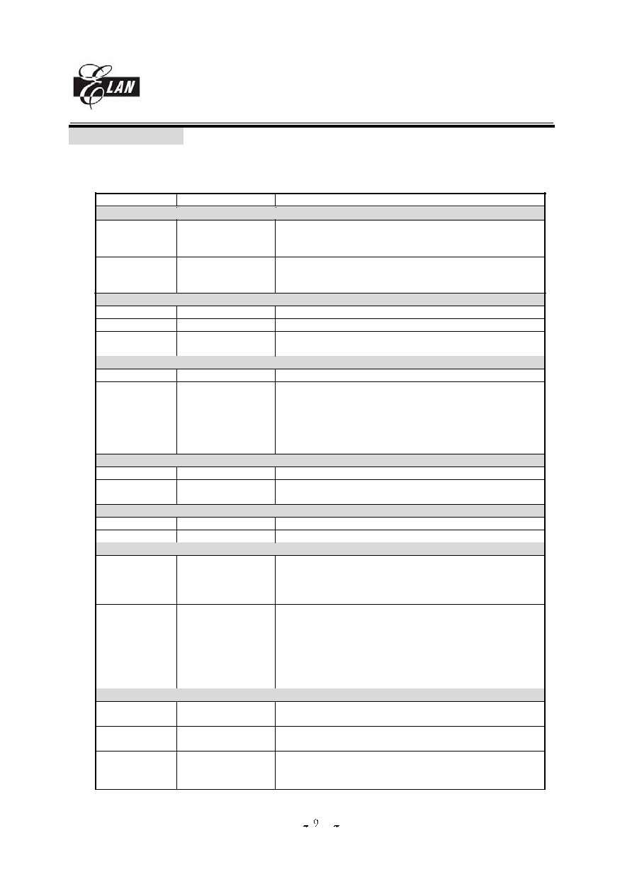
Relative to Rom-less, OTP and Mask
OTP
OTP/ROMLess
OTP
Note
78P911
78P808/78R808
78P915
Operation voltage
2.5~5.5V(normal mode) 2.2~5.5V(normal mode) 2.2V~5.5V(normal mode)
Work clock (Max)
3.58MHz
10.74MHz
10.74MHz
OP
X
Yes
X
Comparator
CMP1
CMP1, 2, 3
CMP1
Key tone
X
Yes
X
External INT
INT0~3
INT0~2
INT0, INT2
LCD
SEG0~59,
COM0~15
SEG0~79
COM0~23
SEG0~27,
SEG48~SEG79,
COM0~15
Data Rom
X
256K*8
X
RAM size
2.5K*8
8K*8
2.5K*8
Programmable ROM
16K*13
32K*13
32K*13
SDT
X
X
Yes
Stack
8
32
8
Bi-directional port
36
51
44
DTMF generator
Yes
TONE generator
Current D/A
DTMF receiver
X
Yes
Yes
Current D/A
X
Yes
Yes
MEI/RTF
X
X
X
Call waiting
Yes
Yes
Yes
Low battery detect
Yes
Comparator
Comparator
SPI
X
Yes
Yes
FSK decode
Yes
Yes
Yes

EM78P915
8-bit Micro-controller
__________________________________________________________________________________________________________________________________________________________________
* This specification is subject to be changed without notice.
2005/12/21 (V2.0)
User Guide
(Before using this chip, take a look at the following description note, it includes important messages.)
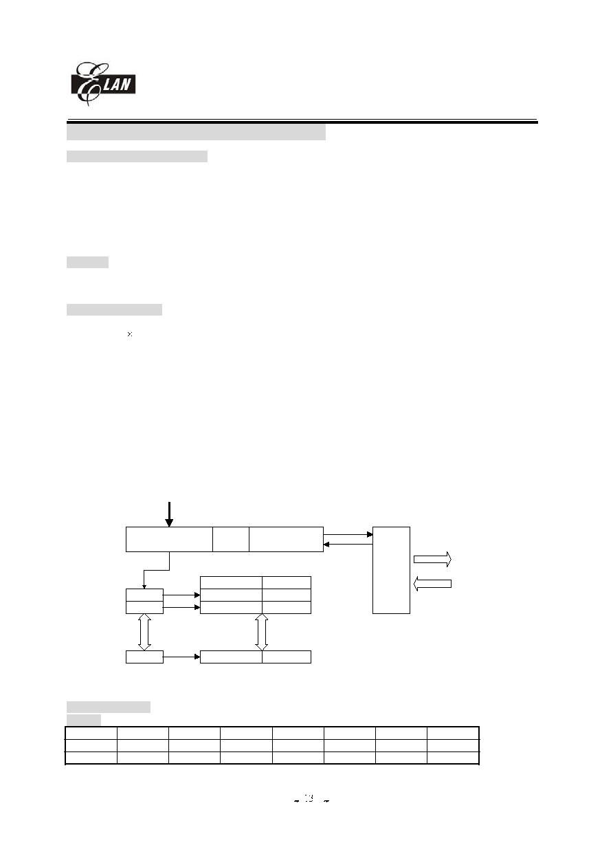
1. You will see some names for the register bits definitions. Some name will be appeared very frequently in the whole spec.
The following describes the meaning for the register's definitions such as bit type, bit name, bit number and so on.
7
6
5
4
3
2
1
0
RAB7
RAB6
BAB5
RAB4
RAB2
RAB0
R/W-0
R/W-0
R-1
R/W-1
R
R/W
Bit type
Bit name
Bit number (7 is MSB, 0 is LSB)
read/write
(default value=0)
read/write
(default value=1)
read only
(w/o default value)
read/write
(w/o default value)
PAGE0
RA
Register name and its page,
RA PAGE0 represents address
0x0A of register page 0
X
RAB1
(undefined) not allowed to use
R-0
read only
(default value=0)
read only
(default value=1)
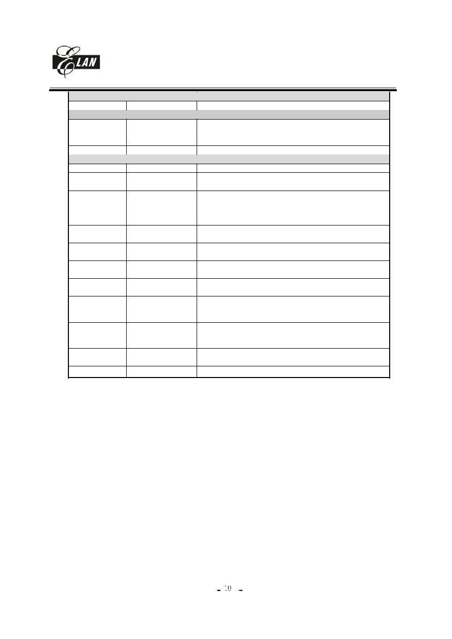
Figure 1, Register overview description
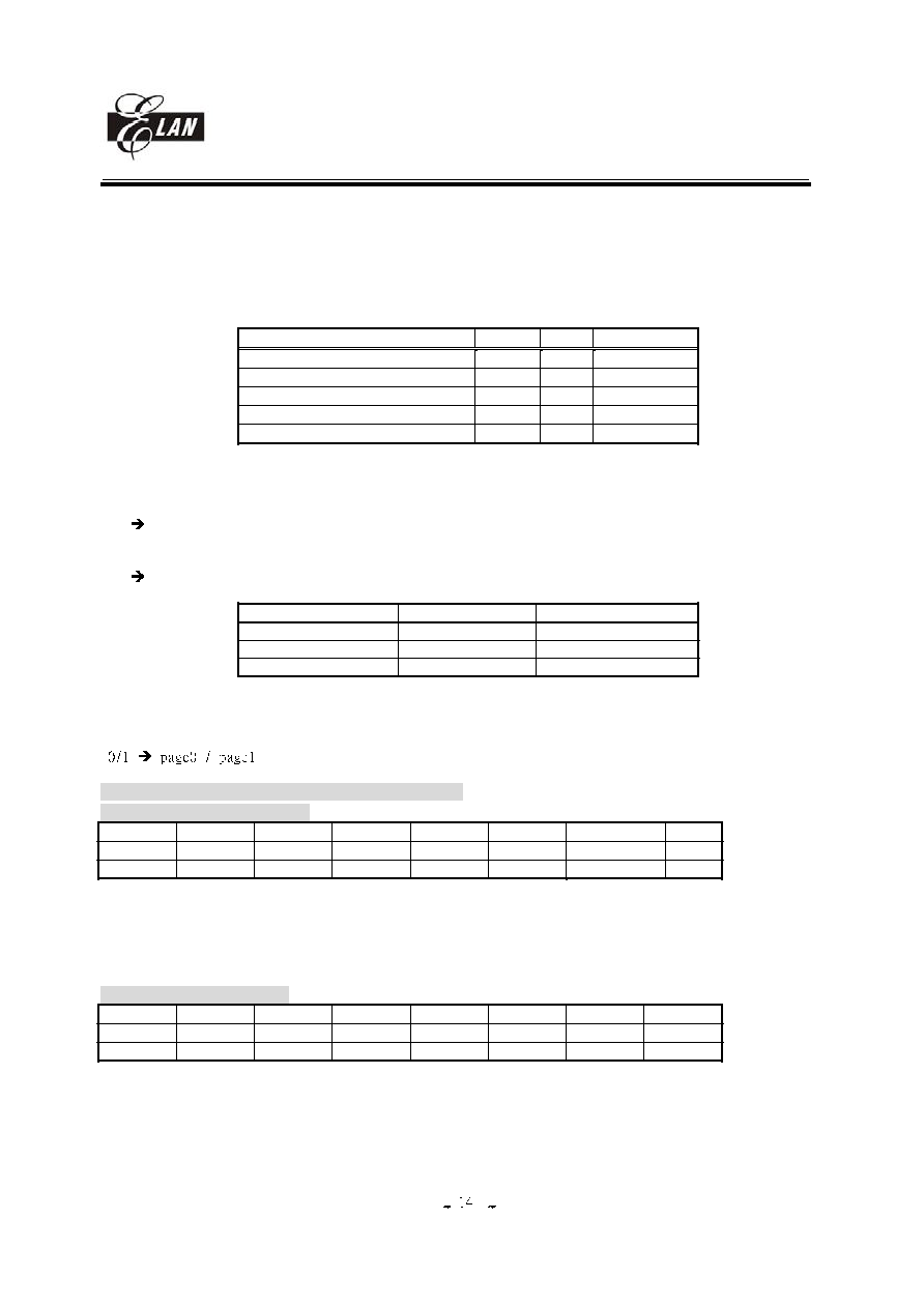
2. There are some undefined bits in the registers. The values in these bits are unpredicted. These bits are not allowed to
use. We use the symbol "X" in the spec to recognize them. A fixed value must be written in some specific unused
bits by software or some unpredicted wrong will occur.
These bits are as below.
Register
Register
PAGE
Bit
Default value
Initial Setting value
Effect
R5
0
7
0
0
Power consumption increase
R6
0
7
0
0
Power consumption increase
R6
1
7~0
00000000
00000000
Un-expect error
R7
0
6~4
000
000
Un-expect error
R7
1
7~0
00000000
00000000
Un-expect error
R8
1
7~0
00000000
00000000
Un-expect error
R9
1
7~0
00000000
00000000
Un-expect error
RE
0
6~5
00
00
Power consumption increase
RE
1
5~4
00
00
Un-expect error
IOC5
0
7
0
0
Power consumption increase
IOC5
1
7~5
000
000
Power consumption increase
IOC5
2
7~0
00000000
00000000
Un-expect error
IOC6
0
7,5~4
0,01
0,01
Un-expect error
IOC6
2
4~3
00
00
Power consumption increase
IOC7
0
6~4
111
111
Un-expect error
IOC7
1
7~0
00000000
00000000
Un-expect error
IOC8
1
7~0
00000000
00000000
Un-expect error
IOCA
1
6~4
111
111
Power consumption increase
IOCB
1
7,5~4
0,01
0,01
Power consumption increase
IOCD
1
7~0
00000000
00000000
Power consumption increase
IOCE
1
1~0
00
00
Power consumption increase
IOCE
1
7~4
000
000
Un-expect error
Table 1, initial setting reference in using ICE915
EM78P915
8-bit Micro-controller
__________________________________________________________________________________________________________________________________________________________________
* This specification is subject to be changed without notice.
2005/12/21 (V2.0)
3. In the appendix, it provides all operational/special purpose registers, figures and tables list for user to search quickly.
4. While switching main clock (regardless of high freq to low freq or on the other hand), adding 6 instructions delay (NOP) is
required.
5. Please do not switch MCU operation mode from normal mode to sleep mode directly. Before into idle or sleep mode,
please switch MCU to green mode.
6. For DATA RAM least address (A0~A7), when using "INC" instruction and overflow occur, the middle address will
auto_increase. If using "DEC" instruction and least address from 0x00 0xFF, the middle address can't auto_decrease.
7. With increasing frequency of using interrupt, it may be occur interrupt flag loss. But it could be solved by our suggestion.
So for avoiding any instruction loss, please obey the following program way for now, of course, we already start to enable
our production procedure for reducing the possibility of loss.
Suggestion way,
Clear interrupt flag (RF): change "BC" to "MOV".
Example: clear bit0 of RF,
Before
Suggestion now
BC 0x0f, 0x00
MOV a,@0xFE
MOV 0x0f,a
8. In the application, some users need latch interrupt flag during disable interrupt mask register (IOCF), but some users don't
need. In the application of EM78 series, we revise this status to latch. So, users must clear the latch interrupt flag before
enable interrupt mask register. The method how to use instruction is showed as follows,
Example:
IOR
IOCF
MOV RF,A
MOV A,@0x??
IOW
IOCF
9. Code-option setting note: Un-used or empty bit of code-option can't be changed to 0. So, please keep them in 1 to avoid
some un-prediction occur.
10. /POVD setting note: please confirm whether /POVD will be enable or disable before ordering EM78P915. If users still
couldn't understand, users can get some information from our FAE or sales.
EM78P915
8-bit Micro-controller
__________________________________________________________________________________________________________________________________________________________________
* This specification is subject to be changed without notice.
2005/12/21 (V2.0)
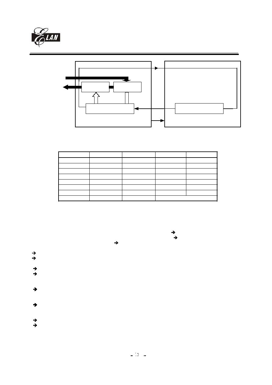
I. General Description
The EM78P915 is an 8-bit CID (Call Identification) RISC type microprocessor with low power, high speed CMOS
technology. Integrated onto a single chip are on chip watchdog (WDT), RAM, ROM, programmable real time clock /counter,
internal interrupt, power down mode, LCD driver, FSK decoder, CALL WAITING decoder, SDT detector, current DA
module and tri-state I/O. The EM78P915 provides a single chip solution to design a CID of calling message display.
II. Feature
CPU
Operating voltage: 2.2V~5.5V for normal mode
Main CLK (Hz)
Under
0.895M~3.58M
10.74M
Operating Voltage (min)
2.2V
3.1V
2.2V~5.5V for green mode
32K 13 on chip program ROM
2.5K 8 on chip RAM
Up to 44 bi-directional tri-state I/O ports
8 level stack for subroutine nesting
8-bit real time clock/counter (TCC)
Two independent 8 bits up-counter interrupt.
Selective signal sources and trigger edges , and with overflow interrupt
Programmable free running on chip watchdog timer
99.9 single instruction cycle commands
4 step Normal mode CLK : 0.895 , 1.79 , 3.58 , 10.74 MHz generated by internal PLL.
Four operation modes.
1. Sleep mode: CPU and PLL turn off, 32.768KHz clock turn off
2. Idle mode: CPU and PLL turn off, 32.768KHz clock turn on
3. Green mode: PLL turn off, CPU and 32.768KHz clock turn on
4. Normal mode: PLL turn on, CPU and 32.768KHz clock turn on
Universal Low battery detector
Input port wake up function
9 interrupt source, 6 external, 3 internal
Port key scan function
Clock frequency 32.768KHz
oscillator start to stable time will smaller/equal 0.5 sec
SPI
Serial Peripheral Interface (SPI) : a kind of serial I/O interface
Interrupt flag available for the read buffer full or transmitter buffer empty.
Programmable baud rates of communication
Three-wire synchronous communication.(shared with IO )
CID
Operation Voltage 2.4V 5.5V for FSK
Operation Voltage 2.4V 5.5V for DTMF receiver
Compatible with Bellcore GR-30-CORE (formerly as TR-NWT-000030)
Compatible with British Telecom (BT) SIN227 & SIN242
FSK demodulator for Bell 202 and ITU-T V.23 (formerly as CCITT V.23)
CALL WAITING
Operation Voltage 2.4V 5.5V
Compatible with Bell-core special report SR-TSV-002476
Call-Waiting (2130Hz plus 2750Hz) Alert Signal Detector
Good talk-down and talk-off performance
Sensitivity compensated by adjusting input OP gain

EM78P915
8-bit Micro-controller
__________________________________________________________________________________________________________________________________________________________________
* This specification is subject to be changed without notice.
2005/12/21 (V2.0)
LCD
LCD operation voltage chosen by software
Common driver pins : 16
Segment driver pins : 60
1/4 bias
1/8,1/16 duty
Current D/A
Operation Voltage 2.2V~5.5V
10-bit resolution and 3-bit output level
Current D/A output can drive speaker through a transistor for sound player
Can switch output port between DAOUT1 and DAOUT2 by user
SDT (Stutter Dial Tone)
TIA/EIA-855 compatible Stutter Dial Tone detector.
Detect the dual frequencies (350Hz and 440Hz) of SDT signal.
PACKAGE
None, but only for COB
III. Application
1. adjunct units
2. answering machines
3. feature phones
EM78P915
8-bit Micro-controller
__________________________________________________________________________________________________________________________________________________________________
* This specification is subject to be changed without notice.
2005/12/21 (V2.0)
IV. Pin Configuration
VDD
XIN
XOUT
VDD
PLLC11
RING1
TIP1
EGIN2
EGIN1
GND
GND
P56
P55
VDTBH
16
17
18
19
20
21
22
23
24
25
26
27
28
29
30
VDTBL
3
1
3
9
4
0
4
1
4
2
4
3
4
4
4
5
4
6
4
7
4
8
4
9
5
0
5
1
5
2
5
3
5
4
5
5
5
6
5
7
5
8
5
9
68
69
70
71
72
73
74
75
76
77
78
79
80
81
82
83
84
85
86
87
88
89
90
91
92
93
94
95
96
9
7
9
8
9
9
1
0
0
1
0
1
1
0
2
1
0
3
1
0
4
1
0
5
1
0
6
1
0
7
1
0
8
1
0
9
1
1
0
1
1
1
1
1
2
1
1
3
1
1
4
1
1
5
1
1
6
1
1
7
1
1
8
1
1
9
1
2
0
1
2
1
1
2
2
1
2
3
1
2
4
1
2
5
1
2
6
1
2
7
1
2
8
1
2
3
4
5
6
D
A
O
U
T
2
P
6
6
P
6
3
P
6
2
P
6
1
P
6
0
T
E
S
T
1
R
E
S
E
T
P
7
7
P
7
3
P
7
2
P
7
1
P
7
0
P
9
7
P
9
6
P
9
5
P
9
4
P
9
3
P
9
2
P
9
1
P
9
0
P
8
7
P86
P85
P84
P83
P82
P81
P80
PC7
PC6
PC5
PC4
PC3
PC2
PC1
PC0
PB7
PB6
PB5
PB4
PB3
PB2
PB1
PB0
SEG27
SEG26
SEG25
SEG24
SEG23
SEG22
S
E
G
2
1
S
E
G
2
0
S
E
G
1
9
S
E
G
1
8
S
E
G
1
7
S
E
G
1
6
S
E
G
1
5
S
E
G
1
4
S
E
G
1
3
S
E
G
1
2
S
E
G
1
1
S
E
G
1
0
S
E
G
9
S
E
G
8
S
E
G
7
S
E
G
6
S
E
G
5
S
E
G
4
S
E
G
3
S
E
G
2
S
E
G
1
C
O
M
1
5
C
O
M
1
4
C
O
M
1
3
C
O
M
1
2
C
O
M
1
1
C
O
M
1
0
C
O
M
9
C
O
M
8
C
O
M
7
C
O
M
6
C
O
M
5
C
O
M
4
C
O
M
3
C
O
M
2
C
O
M
1
C
O
M
0
S
E
G
0
CWGS
CWIN
Figure 2-1, Pad assignment (for chip)

EM78P915
8-bit Micro-controller
__________________________________________________________________________________________________________________________________________________________________
* This specification is subject to be changed without notice.
2005/12/21 (V2.0)
26
27
28
29
30
31
32
33
34
35
36
37
38
1
2
3
4
5
6
7
8
9
10
11
12
13
14
15
16
17
18
19
20
21
22
23
24
25
1
0
3
1
0
4
1
0
5
1
0
6
1
0
7
1
0
8
1
0
9
1
1
0
1
1
1
1
1
2
1
1
3
1
1
4
1
1
5
1
1
6
1
1
7
1
1
8
1
1
9
1
2
0
1
2
1
1
2
2
1
2
3
1
2
4
1
2
5
1
2
6
1
2
7
1
2
8
78
77
76
75
74
73
72
71
70
69
68
67
66
65
94
93
92
91
90
89
88
87
86
85
84
83
82
81
80
79
100
99
98
97
96
95
101
102
3
9
5
5
5
4
5
3
5
2
5
1
5
0
4
9
4
8
4
7
4
6
4
5
4
4
4
3
4
2
4
1
4
0
5
6
5
7
5
8
5
9
6
0
6
1
6
2
6
3
6
4
COM5
COM4
COM3
COM2
COM1
COM0
VDD
XIN
XOUT
VDD
PLLC
RING
TIP
EGIN2
EGIN1
CWGS
CWIN
GND
GND
P56/EST
P55/STGT
DAOUT2
P
6
6
/
D
A
O
U
T
1
P
6
3
/
C
M
P
1
P
6
2
/
S
D
I
P
6
1
/
S
D
O
P
6
0
/
S
C
K
T
E
S
T
/
R
E
S
E
T
P
7
7
/
I
N
T
2
P
7
3
/
I
N
T
0
P
7
2
/
I
N
T
0
P
7
1
/
I
N
T
0
P
7
0
/
I
N
T
0
P
9
7
/
S
E
G
7
9
P
9
6
/
S
E
G
7
8
P
9
5
/
S
E
G
7
7
P
9
4
/
S
E
G
7
6
P
9
3
/
S
E
G
7
5
P
9
2
/
S
E
G
7
4
P
9
1
/
S
E
G
7
3
P
9
0
/
S
E
G
7
2
P
8
7
/
S
E
G
7
1
P86/SEG70
P85/SEG69
P84/SEG68
P83/SEG67
P82/SEG66
P81/SEG65
P80/SEG64
PC7/SEG63
PC6/SEG62
PC5/SEG61
PC4/SEG60
PC3/SEG59
PC2/SEG58
PC1/SEG57
PC0/SEG56
PB7/SEG55
PB6/SEG54
PB5/SEG53
PB4/SEG52
PB3/SEG51
PB2/SEG50
PB1/SEG49
PB0/SEG48
SEG27
SEG26
SEG25
SEG24
SEG23
SEG22
SEG21
SEG20
SEG19
SEG18
SEG17
SEG16
S
E
G
1
5
S
E
G
1
4
S
E
G
1
3
S
E
G
1
2
S
E
G
1
1
S
E
G
1
0
S
E
G
9
S
E
G
8
S
E
G
7
S
E
G
6
S
E
G
5
S
E
G
4
S
E
G
3
S
E
G
2
S
E
G
1
S
E
G
0
C
O
M
1
5
C
O
M
1
4
C
O
M
1
3
C
O
M
1
2
C
O
M
1
1
C
O
M
1
0
C
O
M
9
C
O
M
8
C
O
M
7
C
O
M
6
NC
NC
NC
NC
NC
NC
NC
NC
NC
NC
NC
NC
NC
NC
NC
NC
N
C
N
C
N
C
N
C
N
C
NC
NC
NC
Figure 2-2, Pin assignment (for 128 pin QFP)
Package type: EM78P915AQ BD-GR94261 (/POVD disable), EM78P915BQ BD-GR94262 (/POVD enable)

EM78P915
8-bit Micro-controller
__________________________________________________________________________________________________________________________________________________________________
* This specification is subject to be changed without notice.
2005/12/21 (V2.0)
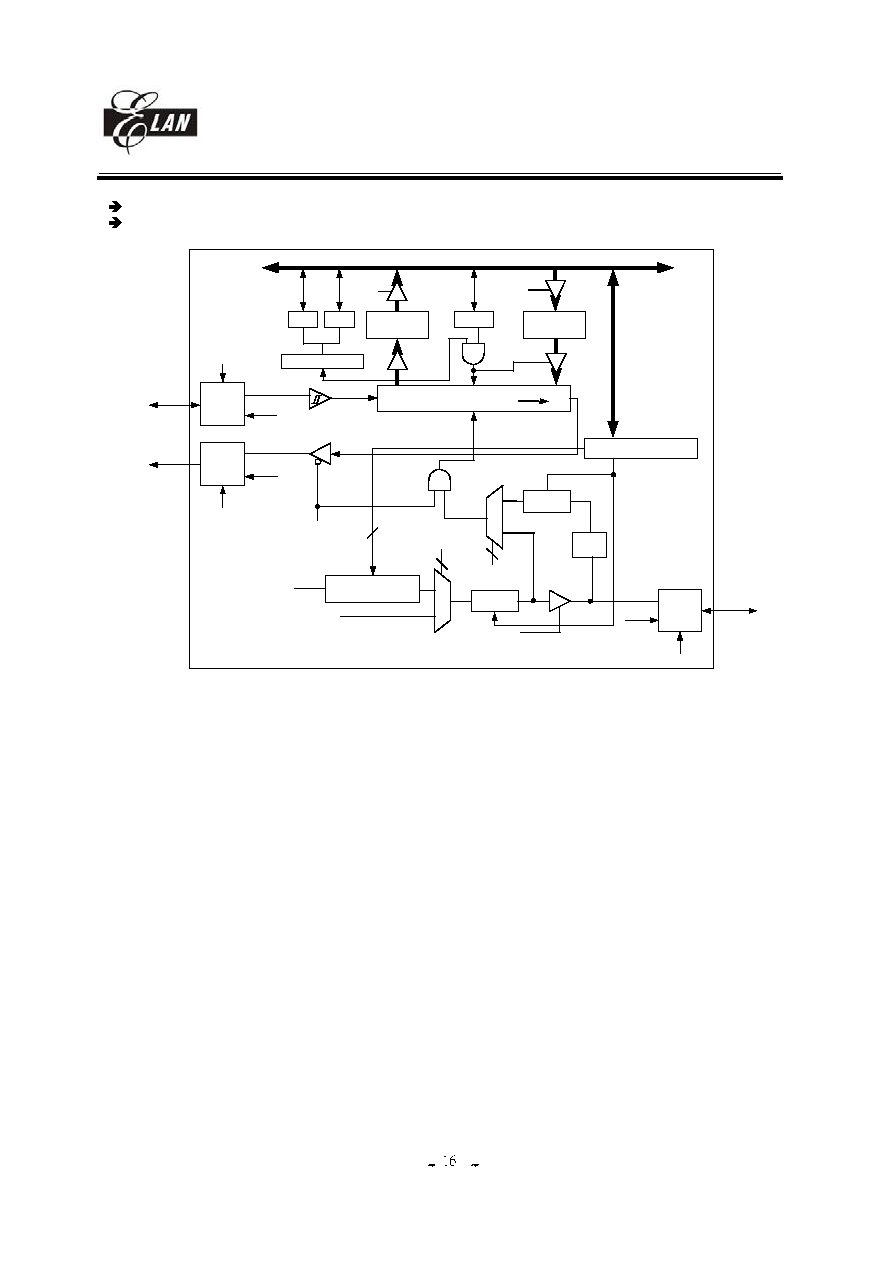
V. Functional Block Diagram
MCU
2.5K x 8
Data RAM
GPIO control
Sub OSC
32.768K Hz
MCLK
XIN
XOUT
PLL
Interrupt
Control
Timer 0
Timer 1
TCC
WDT
LCD driver
120 byte
LCD RAM
COM0~COM15
SEG0~SEG7
SEG8~SEG27
SEG48~SEG55/PB0~PB7
SEG56~SEG63/PC0~PC7
SEG64~SEG71/P80~P87
TIP
RING
FSK
decoder
DTMF
receiver
CW
32K x 13
Program ROM
Comparator
Vin
Pull high
control
GAIN
CWTIP
Current
DA1
SPI
(Serial port)
P60/SCK
P62/SDI
P61/SDO
EST
STGT
SEG72~SEG79/P90~P97
PORT7
P77/INT2
P70~P73/INT0
SDT
detector
DAOUT2
DAOUT1
Figure 3, Block diagram1
EM78P915
8-bit Micro-controller
__________________________________________________________________________________________________________________________________________________________________
* This specification is subject to be changed without notice.
2005/12/21 (V2.0)
VI. Pin Descriptions
PIN
I/O
DESCRIPTION
POWER
VDD
AVDD
POWER
Digital power
Analog power
They connect together when package as 128 pin QFP.
GND
AVSS
POWER
Digital ground
Analog ground
They connect together when package as 128 pin QFP.
CLOCK
XIN
I
Input pin for 32.768 kHz oscillator
XOUT
O
Output pin for 32.768 kHz oscillator
PLLC
I
Phase loop lock capacitor, connect a capacitor 0.01u to 0.047u
with GND
LCD
COM0..COM15
O
Common driver pins of LCD drivers
SEG0..SEG7
SEG8...SEG27
SEG48..SEG55
SEG56..SEG63
SEG64..SEG71
SEG72..SEG79
O
O
O (I/O: PORTB)
O (I/O: PORTC)
O (I/O: PORT8)
O (I/O: PORT9)
Segment driver pins of LCD drivers
SEG48 to SEG79 are shared with IO PORT.
FSK, TONE, KTONE
TIP
I
Should be connected with TIP side of twisted pair lines for FSK.
RING
I
Should be connected with RING side of twisted pair lines for
FSK.
CW
CWGS
O
Gain adjustment of single-ended input OP Amp
CWIN
I
Single-ended input OP Amp for call waiting decoder
DTMF receiver
EST
O
Early steering output. Presents a logic high immediately when the
digital algorithm detects a recognizable tone-pair (signal
condition). Any momentary loss of signal condition will cause
EST to return to a logic low. This pin shared with PORT56.
STGT
I/O
Steering input/guard time output (bi-directional). A voltage
greater than Vtst detected at ST causes the device to register the
detected tone-pair and update the output latch.
A voltage less than Vtst frees the device to accept a new tone-
pair. The GT output acts to reset the external steering time-
constant; its state is a function of EST and the voltage on ST .
This pin shared with PORT55.
SERIAL IO
SCK
IO (PORT60)
Master: output pin, Slave: input pin. This pin shared with
PORT60.
SDO
O (PORT61)
Output pin for serial data transferring. This pin shared with
PORT61.
SDI
I (PORT62)
Input pin for receiving data. This pin shared with PORT62.
EM78P915
8-bit Micro-controller
__________________________________________________________________________________________________________________________________________________________________
* This specification is subject to be changed without notice.
2005/12/21 (V2.0)
Comparator
CMP1
I (PORT63)
Comparator input pins. Shared with PORT63.
CURRENT DA
DAOUT1
O (PORT66)
Current DA output pin. It can be a control signal for sound
generating.
Shared with PORT66.
DAOUT2
O
Current DA output pin.
IO
P55 ~P56
I/O
PORT 5 can be INPUT or OUTPUT port each bit.
P60 ~P63,
P66
I/O
PORT 6 can be INPUT or OUTPUT port each bit.
Internal pull high.
P70 ~ P73, P77
I/O
PORT 7 can be INPUT or OUTPUT port each bit.
Internal Pull high function.
Auto key scan function.
Interrupt function.
P80 ~ P87
I/O
PORT 8 can be INPUT or OUTPUT port each bit.
Shared with LCD Segment signal.
P90 ~ P97
I/O
PORT 9 can be INPUT or OUTPUT port each bit.
Shared with LCD Segment signal.
PB0 ~ PB7
I/O
PORT B can be INPUT or OUTPUT port each bit.
Shared with LCD Segment signal.
PC0 ~ PC7
I/O
PORT C can be INPUT or OUTPUT port each bit.
Shared with LCD Segment signal.
INT0
PORT70...73
Interrupt sources, which has the same interrupt flag. Any pin from
PORT70 to PORT73 has a falling edge signal, it will generate a
interruption.
INT2
PORT77
Interrupt source. Once PORT77 has a falling edge or rising edge
signal (controlled by CONT register), it will generate a
interruption.
TEST
I
Test pin into test mode for factory test only. Connect it ground in
application.
/RESET
I
Low reset
EM78P915
8-bit Micro-controller
__________________________________________________________________________________________________________________________________________________________________
* This specification is subject to be changed without notice.
2005/12/21 (V2.0)
VII. Functional Descriptions
VII. 1 Operational Registers
R PAGE 1 register
R PAGE 0 register
R0
R1 (TCC buffer)
R2 (progam counter)
R3 (status )
R4 (RSR, bank select)
R5 (port55~56, program ROM page)
R6 (port60~63, 66, /SDT,SDTPWR)
R7 (port70~73, 77)
R8 (port80~87)
R9 (port90~97)
RA (CPU mode, clock, FSK, WDT)
RB (portB0~B7)
RC (port C0~C7)
RD (comparator control)
RE (CAS, key scan, LCD control)
RF (interrupt flag)
R4 (SPI status and control)
R5 (SPI data buffer)
R6 (unused)
R7 (unused)
R8 (unused)
R9 (unused)
RA (LCD RAM address)
RB (LCD data buffer)
RC (DATA RAM data buffer)
RD (DATA RAM address0~7)
RE (DATA RAM address8~11 )
Address
00
01
02
03
04
05
06
07
08
09
0A
0B
0C
0D
0E
0F
Figure 4, operational registers overview
Address
00
01
02
03
04
05
06
07
08
09
0A
0B
0C
0D
0E
0F
Control PAGE 0 register
Control PAGE 1 register
IOC5 (IOC55, 56, P8S,P9S,PBS, PCS,CASPWR)
IOC6 (port60~63, 66 IO setting)
IOC7 (port70~73, 77 IO setting)
IOC8 (port80~87 IO setting)
IOC9 (port90~97 IO setting)
IOCA (counter1, 2 prescale and source)
IOCB (portB0~B7 IO setting)
IOCC (portC0~C7 IO setting)
IOCD (counter 1 preset)
IOCE (counter 2 preset)
IOCF (interrupt mask flag)
IOC5 (LCD bias control, CDAS)
IOC6 (current DA)
IOC7 (Unused)
IOC8 (Unused)
IOC9 (DTMF receiver control)
IOCA (port7 pull high)
IOCB (port6 pull high)
IOCC (DAoutput2 volume control,DAoutput1/2
switch ,DA0~DA2)
IOCD (Unused)
IOCE (comparator IO set)
Control PAGE 2 register
IOC6 (port s/w, CDAL)
IOCE (VRSEL)
IOC5 (Unused)
Figure 5, Special purpose registers overview
Note1: operational register page0/1 and special purpose register page0/1/2 are different from program page0~31.
Note2: in figure 4, R"X" represents that address "X" of register in the operational register page 0/1.
Note3: in figure 5, IOC"X" represents that address "X" of register in the special purpose register page 0/1/2.
EM78P915
8-bit Micro-controller
__________________________________________________________________________________________________________________________________________________________________
* This specification is subject to be changed without notice.
2005/12/21 (V2.0)
Address
10
11
12
13
14
15
16
17
18
19
1A
1B
1C
1D
1E
1F
general purpose regigter 10
general purpose regigter 11
general purpose regigter 12
general purpose regigter 13
general purpose regigter 14
general purpose regigter 15
general purpose regigter 16
general purpose regigter 17
general purpose regigter 18
general purpose regigter 19
general purpose regigter 1A
general purpose regigter 1B
general purpose regigter 1C
general purpose regigter 1D
general purpose regigter 1E
general purpose regigter 1F
Figure 6, general purpose registers 10 ~ 1F
20
21
22
3E
3F
Address
Bank 0
general purpose regigter 20
general purpose regigter 21
general purpose regigter 22
general purpose regigter 3E
general purpose regigter 3F
Bank 1
general purpose regigter 20
general purpose regigter 21
general purpose regigter 22
general purpose regigter 3E
general purpose regigter 3F
.
.
.
.
.
.
.
.
.
.
.
.
.
.
.
Bank 2
general purpose regigter 20
general purpose regigter 21
general purpose regigter 22
general purpose regigter 3E
general purpose regigter 3F
.
.
.
.
.
Bank 3
general purpose regigter 20
general purpose regigter 21
general purpose regigter 22
general purpose regigter 3E
general purpose regigter 3F
.
.
.
.
.
Figure 7, general purpose registers 20 ~ 3F in Bank0/1/2/3
In figure 4 and 5, if user want to read/write one or more of these registers to enable some functions, user must take care of
the page number of operational register page and special purpose register page. It must be changed to the proper page number
to avoid read/write error occurring.
In figure 6, general purpose registers 10~1F can be read/write anytime without changing operational register pages and
special purpose register pages.
In figure 7, general purpose registers 20~3F are the similar to general purpose registers 10~1F, but user must take care of
bank0/1/2/3 to avoid read/write error occurring.
EM78P915
8-bit Micro-controller
__________________________________________________________________________________________________________________________________________________________________
* This specification is subject to be changed without notice.
2005/12/21 (V2.0)
VII. 2 Operational Registers Detail descriptions
R0 (Indirect Addressing Register)
R0 is not a physically implemented register. It is useful as indirect addressing pointer. Any instruction using R0 as
register actually accesses data pointed by the RAM Select Register (R4).
Example:
MOV
a, @ 0x20
;store a address at R4 for indirect addressing
MOV 0x04,A
MOV
a, @ 0xAA
;write data 0xAA to R20 at bank0 through R0
MOV 0x00,A
R1 (TCC)
TCC Data buffer. Increased by 16.38KHz or by the instruction cycle clock (controlled by CONT register).
Written and read by the program as any other register.
R2 (Program Counter)
The structure is depicted in Figure. 6.
Generates 32K 13 on-chip PROGRAM ROM addresses to the relative programming instruction codes.
"JMP" instruction allows the direct loading of the low 10 program counter bits.
"CALL", this instruction loads the low 10 bits of the PC, PC+1, and then push into the stack.
"RET'' ("RETL k", "RETI") instruction loads the program counter with the contents at the top of stack.
"MOV R2, A" allows the loading of an address from the A register to the PC, and the ninth and tenth bits are cleared to
"0''.
"ADD R2, A" allows a relative address be added to the current PC, and contents of the ninth and tenth bits are cleared to
"0''.
"TBL" allows a relative address be added to the current PC, and contents of the ninth and tenth bits don't change. The
most significant bit (A10~A14) will be loaded with the content of bit PS0~PS3 in the status register (R5) upon the
execution of a "JMP'', "CALL'', "ADD R2, A'', or "MOV R2, A'' instruction.
If a interrupt trigger, PROGRAM ROM will jump to address8 at page0. The CPU will store ACC, R3 status and R5 PAGE
automatically, it will restore after instruction RETI.
A14 A13 A12 A11 A10
A9 A8
A7 ~ A0
PC
stack 1
stack 2
.
.
.
stack 7
stack 8
00000
R5 (Program PAGE)
PAGE 0
0000~03FF
Address
PAGE number
00001
PAGE 1
0400~07FF
Mapping
11111
PAGE 31
7C00~7FFF
CALL and
interrupt
store
restore
ACC, R3 and
R5(program PAGE)
Figure 8, program counter organization
R3 (Status Register)
PAGE 0
7
6
5
4
3
2
1
0
PAGE
IOCP1S
IOCPAGE
T
P
Z
DC
C
R/W-0
R/W-0
R/W-0
R/W-X
R/W-X
R/W-X
R/W-X
R/W-X
EM78P915
8-bit Micro-controller
__________________________________________________________________________________________________________________________________________________________________
* This specification is subject to be changed without notice.
2005/12/21 (V2.0)
Bit 0 (C): Carry flag
Bit 1 (DC): Auxiliary carry flag
Bit 2 (Z): Zero flag
Bit 3 (P): Power down bit.
Set to 1 during power on or by a "WDTC" command and reset to 0 by a "SLEP" command.
Bit 4 (T): Time-out bit.
Set to 1 by the "SLEP" and "WDTC" command, or during power up and reset to 0 by WDT timeout.
EVENT
T
P
REMARK
WDT wake up from sleep mode
0
0
WDT time out (not sleep mode)
0
1
/RESET wake up from sleep
1
0
Power up
1
1
Low pulse on /RESET
x
x
x : don't care
Table 2, Event for power down bit and timer out bit
Bit 5(IOCPAGE): change IOC5 ~ IOCE to another page
Please refer to Fig.4 control register configuration for details.
0/1 page0 / page1
Bit 6(IOCP1S): change IOC PAGE1 and PAGE2 to another option register
Please refer to Fig.4 control register configuration for details.
0/1 page1 /page2
Bit 6(IOCP1S)
Bit 5 (IOCPAGE)
PAGE SELECT
X
0
PAGE 0
0
1
PAGE 1
1
1
PAGE 2
Table 3, relation with IOCP1S bit and IOCPAGE bit
Bit 7(PAGE): change R4 ~ RE to another page
Please refer to Fig.4 control register configuration for details.
R4 (RAM selection for common registers R20 ~ R3F, SPI)
PAGE 0 (RAM selection register)
7
6
5
4
3
2
1
0
RB1
RB0
RSR5
RSR4
RSR3
RSR2
RSR1
RSR0
R/W-0
R/W-0
R/W-X
R/W-X
R/W-X
R/W-X
R/W-X
R/W-X
Bit 0 ~ Bit 5 (RSR0 ~ RSR5): Indirect addressing for common registers R20 ~ R3F
RSR bits are used to select up to 32 registers (R20 to R3F) in the indirect addressing mode.
Bit 6 ~ Bit 7 (RB0 ~ RB1): Bank selection bits for common registers R20 ~ R3F
These selection bits are used to determine which bank is activated among the 4 banks for 32 register (R20 to R3F)..
Please refer to Fig.4 control register configuration for details.
PAGE 1 (SPI control register)
7
6
5
4
3
2
1
0
RBF
SPIE
SRO
SE
SCES
SBR2
SBR1
SBR0
R-0
R/W-0
R/W-0
R/W-0
R/W-0
R/W-0
R/W-0
R/W-0
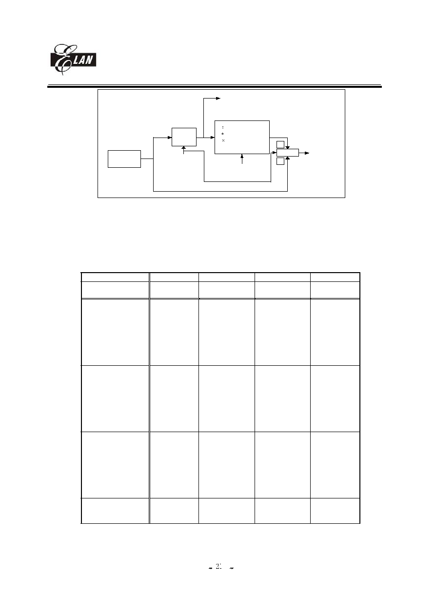
Fig. 6 shows how SPI to communicate with other device by SPI module. If SPI is a master controller, it sends clock through
the SCK pin. An 8-bit data is transmitted and received at the same time. If SPI, however, is defined as a slave, its SCK pin
could be programmed as an input pin. Data will continue to be shifted on a basis of both the clock rate and the selected edge.
EM78P915
8-bit Micro-controller
__________________________________________________________________________________________________________________________________________________________________
* This specification is subject to be changed without notice.
2005/12/21 (V2.0)
Bit 0
SPI module
SCK
Bit7
Salve Device
SPIR register
SDI
SPIW register
SPIS Reg
SDO
SDO
SCK
SDI
Master Device
R5 page1
SPI data buffer
Figure 9, Single SPI Master / Salve Communication
Bit 0 ~ Bit 2 (SBR0 ~ SBR2): SPI baud rate selection bits
SBR2
SBR1
SBR0
Mode
Baud rate
0
0
0
Master
Fsco
0
0
1
Master
Fsco/2
0
1
0
Master
Fsco/4
0
1
1
Master
Fsco/8
1
0
0
Master
Fsco/16
1
0
1
Master
Fsco/32
1
1
0
Slave
1
1
1
X
Table 4, SPI baud rate selection
<Note> Fsco = CPU instruction clock
For example:
If PLL enable and RA PAGE0 (Bit5, Bit4)=(1,1), instruction clock is 3.58MHz/2
Fsco=3.5862MHz/2
If PLL enable and RA PAGE0 (Bit5, Bit4)=(0,0), instruction clock is 0.895MHz/2
Fsco=0.895MHz/2
If PLL disable, instruction clock is 32.768kHz/2
Fsco=32.768kHz/2.
Bit 3 (SCES): SPI clock edge selection bit
1 Data shifts out on falling edge, and shifts in on rising edge. Data is hold during the high level.
0 Data shifts out on rising edge, and shifts in on falling edge. Data is hold during the low level.
Bit 4 (SE): SPI shift enable bit
1
Start to shift, and keep on 1 while the current byte is still being transmitted.
0
Reset as soon as the shifting is complete, and the next byte is ready to shift.
<Note>: This bit has to be reset in software.
Bit 5 (SRO): SPI read overflow bit
1
A new data is received while the previous data is still being hold in the SPIB register. In this situation, the data in SPIS
register will be destroyed. To avoid setting this bit, users had better to read SPIB register even if the transmission is
implemented only.
0
No overflow
<Note>: This can only occur in slave mode.
Bit 6 (SPIE): SPI enable bit
1
Enable SPI mode
0
Disable SPI mode
EM78P915
8-bit Micro-controller
__________________________________________________________________________________________________________________________________________________________________
* This specification is subject to be changed without notice.
2005/12/21 (V2.0)
Bit 7 (RBF): SPI read buffer full flag
1
Receive is finished, SPIB is full.
0
Receive is not finish yet, SPIB is empty.
SPIS reg.
Read
R5
Write
R5
SPIR reg.
Edge
Select
shift right
bit 0
bit 7
Prescaler
4, 8, 16, 32, 64, 128
PORT62
PORT61
SCK
T
sco
16.38kHz
SBR2~SBR0
3
Clock Select
2
Noise
Filter
SPIC reg. (R4 page1)
SBR0 ~SBR2
RBF
RBFI
Buffer Full Detector
set to 1
SPIWC
SDO
SPIE
SDI
MUX
SPIE
0
PORT60
MUX
SCK
SPIE
3
SPIW reg.
Edge
Select
MUX
SDI/P62
SDO/P61
SCK/P60
Figure 10, SPI structure
SPIC reg.: SPI control register
SDO/P61: Serial data out
SDI/P62: Serial data in
SCK/P60: Serial clock
RBF: Set by buffer full detector, and reset in software.
RBFI: Interrupt flag. Set by buffer full detector, and reset in software.
Buffer Full Detector: Sets to 1, while an 8-bit shifting is complete.
SE: Loads the data in SPIW register, and begin to shift
SPIE: SPI control register
SPIS reg.: Shifting byte out and in. The MSB will be shifted first. Both the SPIS register and the SPIW register are
loaded at the same time. Once data being written to, SPIS starts transmission / reception. The received data
will be moved to the SPIR register, as the shifting of the 8-bit data is complete. The RBF (Read Buffer Full)
flag and the RBFI (Read Buffer Full Interrupt) flag are set.
SPIR reg.: Read buffer. The buffer will be updated the 8-bit shifting is complete. The data must be read before the next
reception is finished. The RBF flag is cleared as the SPIR register read.
SPIW reg.: Write buffer. The buffer will deny any write until the 8-bit shifting is complete. The SE bit will be kept in 1
if the communication is still under going. This flag must be cleared as the shifting is finished. Users can
determine if the next write attempt is available.
SBR2 ~ SBR0: Programming the clock frequency/rates and sources.
Clock select: Selecting either the internal instruction clock or the external 16.338KHz clock as the shifting clock.
Edge Select: Selecting the appropriate clock edges by programming the SCES bit
EM78P915
8-bit Micro-controller
__________________________________________________________________________________________________________________________________________________________________
* This specification is subject to be changed without notice.
2005/12/21 (V2.0)
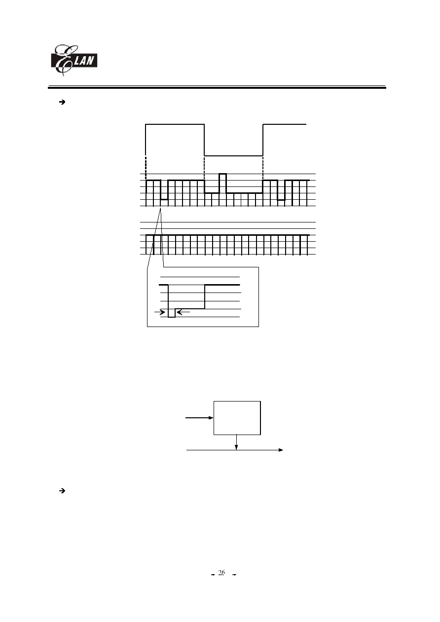
SDO
RBF
SCK
(SCES=0)
SCK
(SCES=1)
SDI
Shift data out
Shift data in
Clear by software
Bit7
Bit6
Bit5
Bit4
Bit3
Bit2
Bit1
Bit0
Figure 11, SPI timing
R5 (PORT5 I/O data, Program page selection, SPI data)
PAGE 0 (PORT5 I/O data register, Program page register)
7
6
5
4
3
2
1
0
X
R56
R55
PS4
PS3
PS2
PS1
PS0
R/W-0
R/W-0
R/W-0
R/W-0
R/W-0
R/W-0
R/W-0
Bit 0 ~ Bit 4 (PS0 ~ PS4): Program page selection bits
PS4
PS3
PS2
PS1
PS0 Program memory page (Address)
0
0
0
0
0
Page 0
0
0
0
0
1
Page 1
0
0
0
1
0
Page 2
0
0
0
1
1
Page 3
:
:
:
:
:
:
:
:
:
:
:
:
1
1
1
1
0
Page 30
1
1
1
1
1
Page 31
Table 5, program page selection
User can use PAGE instruction to change page to maintain program page by user. And the program page is maintained
by EMC's complier. It will change user's program by inserting instructions within program.
Bit 5 ~ Bit 6 (P55 ~ P56): 2-bit PORT55~56 I/O data register
User can use IOC5 page0 register to define input or output each bit.
Bit 7(Unused)
EM78P915
8-bit Micro-controller
__________________________________________________________________________________________________________________________________________________________________
* This specification is subject to be changed without notice.
2005/12/21 (V2.0)
PAGE 1 (SPI data buffer)
7
6
5
4
3
2
1
0
SPIB7
SPIB6
SPIB5
SPIB4
SPIB3
SPIB2
SPIB1
SPIB0
R/W-0
R/W-0
R/W-0
R/W-0
R/W-0
R/W-0
R/W-0
R/W-0
Bit 0 ~ Bit 7 (SPIB0 ~ SPIB7): SPI data buffer
If you write data to this register, the data will write to SPIW register. If you read this data, it will read the data from
SPIR register. Please refer to figure7
R6 (PORT6 I/O data)
PAGE 0 (PORT6 I/O data register)
7
6
5
4
3
2
1
0
X
P66
SDTPWR
/SDT
P63
P62
P61
P60
R/W-0
R/W-0
R
R/W-0
R/W-0
R/W-0
R/W-0
Bit 0 ~ Bit 3, Bit 6 (P60 ~ P63, P66): 8-bit PORT60~63, PORT66 I/O data register
User can use IOC6 page0 register to define input or output each bit.
Bit 4 (/SDT): Data of /SDT, "0" is expressed the valid signal and "1" is expressed the invalid.
Bit 5 (SDTPWR): Control SDT on/off by 1/0.
Bit 7 (Unused)
PAGE 1 (Unused)
7
6
5
4
3
2
1
0
X
X
X
X
X
X
X
X
Bit 0 ~ Bit 7 (Unused)
R7 (PORT7 I/O data)
PAGE 0 (PORT7 I/O data register)
7
6
5
4
3
2
1
0
P77
X
X
X
P73
P72
P71
P70
R/W-0
R/W-0
R/W-0
R/W-0
R/W-0
Bit 0 ~ Bit 4, Bit 7(P70 ~ P73, P77): 8-bit PORT70~74, PORT77 I/O data register
User can use IOC7 page0 register to define input or output each bit.
Bit 4 ~ 6(Unused)
PAGE 1 (Unused)
7
6
5
4
3
2
1
0
X
X
X
X
X
X
X
X
Bit 0 ~ Bit 7 (Unused)
R8 (PORT8 I/O data)
PAGE 0 (PORT8 I/O data register)
7
6
5
4
3
2
1
0
P87
P86
P85
P84
P83
P82
P81
P80
R/W-0
R/W-0
R/W-0
R/W-0
R/W-0
R/W-0
R/W-0
R/W-0
Bit 0 ~ Bit 7 (P80 ~ P87): 8-bit PORT8 ( 0~7 ) I/O data register
User can use IOC8 page0 register to define input or output each bit.
PAGE 1 (Unused)
7
6
5
4
3
2
1
0
X
X
X
X
X
X
X
X
Bit 0 ~ Bit 7 (Unused)
EM78P915
8-bit Micro-controller
__________________________________________________________________________________________________________________________________________________________________
* This specification is subject to be changed without notice.
2005/12/21 (V2.0)
R9 (PORT9 I/O data)
PAGE 0 (PORT9 I/O data register)
7
6
5
4
3
2
1
0
P97
P96
P95
P94
P93
P92
P91
P90
R/W-0
R/W-0
R/W-0
R/W-0
R/W-0
R/W-0
R/W-0
R/W-0
Bit 0 ~ Bit 7 (P90 ~ P97): 8-bit PORT9 (0~7 ) I/O data register
User can use IOC9 page0 register to define input or output each bit.
PAGE 1 (Unused)
7
6
5
4
3
2
1
0
X
X
X
X
X
X
X
X
Bit 0 ~ Bit 7 (Unused)
RA (CPU power saving, PLL, Main clock selection, FSK, Watchdog timer, LCD address)
PAGE 0 (CPU power saving bit, PLL, Main clock selection bits, FSK, Watchdog timer enable bit)
7
6
5
4
3
2
1
0
IDLE
PLLEN
CLK1
CLK0
FSKPWR FSKDATA
/CD
WDTEN
R/W-0
R/W-0
R/W-0
R/W-0
R/W-0
R
R
R/W-0
Bit 0 (WDTEN): Watch dog control register
User can use WDTC instruction to clear watch dog counter. The counter 's clock source is 32768/2 Hz. If the prescaler
assigns to TCC. Watch dog will time out by (1/32768)*2 * 256 = 15.616ms. If the prescaler assigns to WDT, the time of
time out will be more times depending on the ratio of prescaler.
0/1 disable/enable
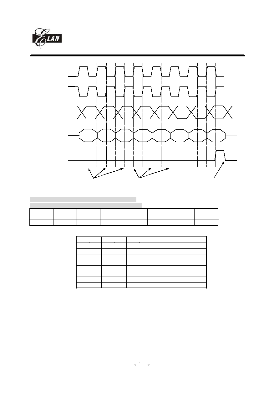
Bit 1 (/CD): FSK carrier detect indication
0/1 Carrier Valid/Carrier Invalid
It's a read only signal. If FSK decoder detect the energy of mark or space signal. The Carrier signal will go to low level.
Otherwise it will go to high.. Note!! Should be at normal mode.
Bit 2 (FSKDATA): FSK decoding data output
It's a read only signal. If FSK decode the mark or space signal , it will output high level signal or low level signal at this
register. It's a raw data type. That means the decoder just decode the signal and has no process on FSK signal. Note!!
Should be at normal mode.
User can use FSK data falling edge interrupt function to help data decoding.
Ex:
MOV A,@01000000
IOW IOCF
;enable FSK interrupt function
CLR RF
ENI
;wait for FSK data's falling edge
:
0 = Space data ( 2200Hz )
1 = Mark data (1200Hz)
Bit 3 (FSKPWR): FSK power control
0/1 FSK decoder powered down / FSK decoder powered up
It's the control register of FSK block power.
The relation between bit 1 to bit 3 is shown in Figure.10. You have to power FSK decoder up first, then wait a setup time
(Tsup) and check carrier signal (/CD). If the carrier is low, program can process the FSK data.
EM78P915
8-bit Micro-controller
__________________________________________________________________________________________________________________________________________________________________
* This specification is subject to be changed without notice.
2005/12/21 (V2.0)
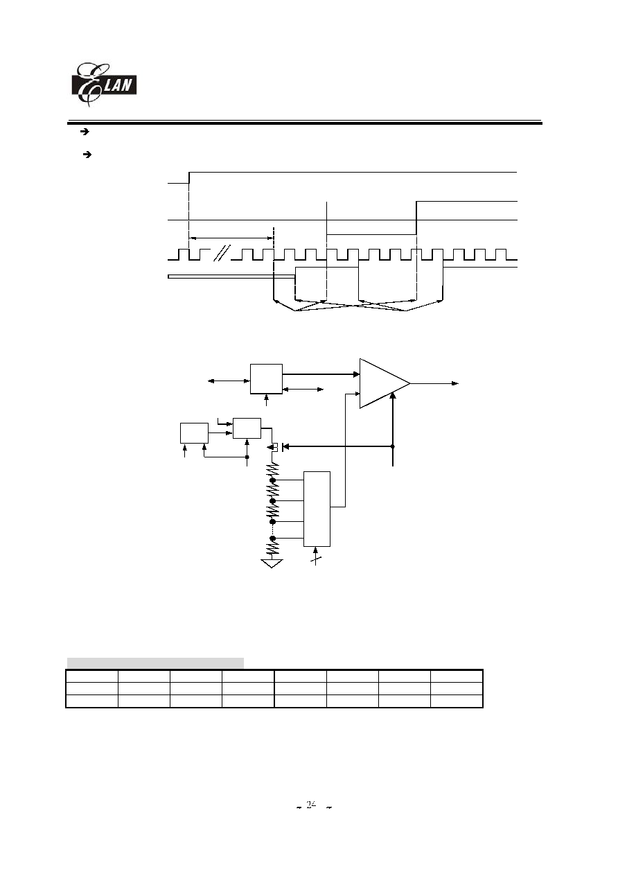
TIP/RING
/CD
FSKDATA
FIRST RING
2 SECONDS
0.5 SEC
0.5 SEC
SECOND RING
2 SECONDS
DATA
Tcdl
/FSKPWR
Tdoc
Tcdh
Tsup
FSK signal
Figure 12, the relation between bit 1 ~ bit 3 of FSK in RA
The controller is a CMOS device designed to support the Caller Number Deliver feature which is offered by the
Regional Bell Operating Companies. The FSK block comprises one path: the signal path. The signal path consist of an
input differential buffer, a band pass filter, an FSK demodulator and a data valid with carrier detect circuit.
In a typical application, user can use his own external ring detect output as a triggering input to IO port. User can use
this signal to wake up whole chip by external ring detect signal.
By setting "1" to bit 3 (FSKPWR) of register RA to activate the block of FSK decoder. If bit 3 (FSKPWR) of register
RA is set to "0", the block of FSK decoder will be powered down.
The input buffer accepts a differential AC coupled input signal through the TIP and RING input and feeds this signal to
a band pass filter. Once the signal is filtered, the FSK demodulator decodes the information and sends it to a post filter.
The output data is then made available at bit 2 (FSKDATA) of register RA. This data, as sent by the central office,
includes the header information (alternate "1" and "0") and 150 ms of marking which precedes the date, time and calling
number. If no data is present, the bit 2 (DATA) of register RA is held on "1" state. This is accomplished by an carrier
detect circuit which determines if the in-band energy is high enough. If the incoming signal is valid, bit 1 (/CD) of
register RA will be "0" otherwise it will be held on "1". And thus the demodulated data is transferred to bit 2 (DATA) of
register RA. If it is not, then the FSK demodulator is blocked.
Bit 4 ~ Bit 5 (CLK0 ~ CLK1): Main clock selection bits
User can choose different frequency of main clock by CLK1 and CLK2. All the clock selection is list below.
PLLEN
CLK1
CLK0
Sub clock
MAIN clock
CPU clock
1
0
0
32.768kHz
895.658kHz
895.658kHz (Normal mode)
1
0
1
32.768kHz
1.7913MHz
1.7913MHz (Normal mode)
1
1
0
32.768kHz
10.7479MHz 10.7479MHz (Normal mode)
1
1
1
32.768kHz
3.5826MHz
3.5826MHz (Normal mode)
0
Don't care don't care
32.768kHz
Don't care
32.768kHz (Green mode)
0
Don't care don't care
32.768kHz
Don't care
32.768kHz (Green mode)
0
Don't care don't care
32.768kHz
Don't care
32.768kHz (Green mode)
0
Don't care don't care
32.768kHz
Don't care
32.768kHz (Green mode)
Table 6, main clock selection
Bit 6 (PLLEN): PLL enable control bit
It is CPU mode control register. If PLL is enabled, CPU will operate at normal mode (high frequency, main clock);
otherwise, it will run at green mode (low frequency, 32768 Hz).
0/1
disable/enable
EM78P915
8-bit Micro-controller
__________________________________________________________________________________________________________________________________________________________________
* This specification is subject to be changed without notice.
2005/12/21 (V2.0)
Sub-clock
32.768kHz
PLL
switch
0
ENPLL
CLK1 ~ CLK0
1
System clock
3.5826MHz to analog circuit
=>895.658kHz
=>1.7913MHz
=>3.5826MHz
=>10.7479MHz
4
2
3
1
Figure 13, the relation between 32.768kHz and PLL
Bit 7 (IDLE): power saving mode control register
When PLL is disable, users can set this bit after using "SLEP" instruction for SLEEP mode or IDLE
mode selection.
0/1 -> SLEEP/IDLE
this bit will decide SLEP instruction which to go.
The status after wake-up and the wake-up sources list as the table below.
Wakeup signal
SLEEP mode
IDLE mode
GREEN mode
NORMAL mode
RA(7,6)=(0,0)
+ SLEP
RA(7,6)=(1,0)
+ SLEP
RA(7,6)=(x,0)
no SLEP
RA(7,6)=(x,1)
no SLEP
TCC time out
IOCF bit 0=1
And "ENI"
No function
(1) wake-up
(2) interrupt
(jump to address 8
at page 0)
(3) after RETI
instruction, jump to
SLEP next
instruction
Interrupt
(jump to address 8
at page0)
Interrupt
(jump to address
8 at page0)
COUNTER1 time out
IOCF bit 1=1
And "ENI"
No function
(1) wake-up
(2) interrupt
(jump to address 8
at page 0)
(3) after RETI
instruction, jump to
SLEP next
instruction
Interrupt
(jump to address 8
at page0)
Interrupt
(jump to address
8 at page0)
COUNTER2 time out
IOCF bit 2=1
And "ENI"
No function
(1) wake-up
(2) interrupt
(jump to address 8
at page 0)
(3) after RETI
instruction, jump to
SLEP next
instruction
Interrupt
(jump to address 8
at page0)
Interrupt
(jump to address
8 at page0)
WDT time out
RESET and
Jump to address
0
(1) wake-up
(2) next instruction
RESET and Jump
to address 0
RESET and
Jump to address
0
EM78P915
8-bit Micro-controller
__________________________________________________________________________________________________________________________________________________________________
* This specification is subject to be changed without notice.
2005/12/21 (V2.0)
PORT7
IOCF bit3 or bit5 = 1
And "ENI"
RESET and
Jump to address
0
(1) wake-up
(2) interrupt
(jump to address 8
at page 0)
(3) after RETI
instruction, jump to
SLEP next
instruction
Interrupt
(jump to address 8
at page0)
Interrupt
(jump to address
8 at page0)
Table 7, sleep/green/normal modes with wake up signal
<Note> Stack overflow interrupt function is exist in ROM less and OTP chip only.
<Note> PORT70 ~ PORT73 's wakeup function is controlled by IOCF bit3 and ENI instruction. They are falling edge
trigger.
PORT77 's wakeup function is controlled by IOCF bit5 and ENI instruction. It's falling edge or rising edge trigger (controlled
by CONT register).
PAGE 1 (LCD address)
7
6
5
4
3
2
1
0
LCDA7
LCDA6
LCDA5
LCDA 4
LCDA 3
LCDA 2
LCDA 1
LCDA 0
R/W-0
R/W-0
R/W-0
R/W-0
R/W-0
R/W-0
R/W-0
R/W-0
Bit 0 ~ Bit 7 (LCDA0 ~ LCDA7): LCD address for LCD RAM reading or writing
The data in the LCD RAM correspond to the COMMON and SEGMENT signals as the table.
COM15 ~COM8
(set R9 PAGE1 bit7=0)
COM7 ~ COM0
(set R9 PAGE1 bit7=0)
Address 80H
Address 00H
SEG0
Address 81H
Address 01H
SEG1
Address 82H
Address 02H
SEG2
:
:
:
Address 9BH
Address 1BH
SEG27
Address 9CH
Address 1CH
Empty
:
:
:
Address AFH
Address 2FH
Empty
Address B0H
Address 30H
SEG48
:
:
:
Address CEH
Address 4EH
SEG78
Address CFH
Address 4FH
SEG79
Address D0H
Address 50H
Empty
:
:
:
Address FFH
Address 7FH
Empty
Table 8, Common/Segment signal
RB (PORTB I/O data, LCD data)
PAGE 0 (PORTB I/O data register)
7
6
5
4
3
2
1
0
PB7
PB6
PB5
PB4
PB3
PB2
PB1
PB0
R/W-0
R/W-0
R/W-0
R/W-0
R/W-0
R/W-0
R/W-0
R/W-0
Bit 0 ~ Bit 7 (PB0 ~ PB7): 8-bit PORTB0~B7 I/O data register
User can use IOCB page0 register to define input or output each bit.
EM78P915
8-bit Micro-controller
__________________________________________________________________________________________________________________________________________________________________
* This specification is subject to be changed without notice.
2005/12/21 (V2.0)
PAGE 1 (LCD data buffer)
7
6
5
4
3
2
1
0
LCDD7
LCDD6
LCDD5
LCDD4
LCDD3
LCDD2
LCDD1
LCDD0
R/W-0
R/W-0
R/W-0
R/W-0
R/W-0
R/W-0
R/W-0
R/W-0
Bit 0 ~ Bit 7 (LCDD0 ~ LCDD7): LCD data buffer for LCD RAM reading or writing
Example.
MOV A, @0
MOV R9_PAGE1, A
MOV RA_PAGE1, A
;ADDRESS
MOV A, @0XAA
MOV
RB_PAGE1, A
;WRITE DATA 0XAA TO LCD RAM
MOV
A, RB_PAGE1
;READ DATA FROM LCD RAM
RC (PORTC I/O data, Data RAM data)
PAGE 0 (PORTC I/O data register)
7
6
5
4
3
2
1
0
PC7
PC6
PC5
PC4
PC3
PC2
PC1
PC0
R/W-0
R/W-0
R/W-0
R/W-0
R/W-0
R/W-0
R/W-0
R/W-0
Bit 0 ~ Bit 7 (PC0 ~ PC7): 8-bit PORTC0~C7 I/O data register
User can use IOCC page0 register to define input or output each bit.
PAGE 1 (Data RAM data buffer)
7
6
5
4
3
2
1
0
RAMD7
RAMD6
RAMD5
RAMD4
RAMD3
RAMD2
RAMD1
RAMD0
R/W-0
R/W-0
R/W-0
R/W-0
R/W-0
R/W-0
R/W-0
R/W-0
Bit 0 ~ Bit 7 (RAMD0 ~ RAMD7): Data RAM data buffer for RAM reading or writing.
Example.
MOV
A , @1
MOV
RD_PAGE1 , A
MOV
A , @0
MOV
RE_PAGE1 , A
MOV
A , @0x55
MOV
RC_PAGE1 , A
;write data 0x55 to DATA RAM which address is "0001".
MOV
A , RC_PAGE1
;read data
RD (Comparator control, Data RAM address (0 ~ 7))
PAGE 0 (Comparator control bits)
7
6
5
4
3
2
1
0
CMPEN
CMPFLAG
CMPS1
CMPS0
CMP_B3
CMP_B2
CMP_B1
CMP_B0
R/W-0
R
R-0
R-0
R/W-0
R/W-0
R/W-0
R/W-0
If user define the PORT63 (by CMPIN1 at IOCE page1) to a comparator input. User can use this register to control
comparator's function.
Bit 0~Bit 3(CMP_B0~CMP_B3): Reference voltage selection of internal bias circuit for comparator.
Reference voltage for comparator =
15
~
0
,
16
5
.
0
n
for
n
VDD
Bit 4~Bit 5(CMPS0~CMPS1): Channel selection to CMP1
CMPS1
CMPS0
Input
0
0
CMP1
Table 9, channel selection of CMP
Bit 6(CMPFALG): Comparator output flag
0
Input voltage < reference voltage
EM78P915
8-bit Micro-controller
__________________________________________________________________________________________________________________________________________________________________
* This specification is subject to be changed without notice.
2005/12/21 (V2.0)
1
Input voltage > reference voltage
Bit 7(CMPEN): Enable control bit of comparator.
0/1
disable/enable, when this bit is set to "0", 2.0V ref circuit is also powered off.
C M P E N
C M P 1
r e f e r e n c e
v o l t a g e
C P U c lo c k
C M P F L A G
S e t u p t i m e 1 0 u s
C o m p a r e s t a r t
C o m p a r e e n d
Figure 14, Comparator timing
+
-
CMPFLAG
CMPEN
PORT63
MUX
CMP1
CMPIN1
P63/CMP1
MUX
1/2R
R
R
1/2R
4
CMP_B3 to CMP_B0
1111
1110
0000
VRSEL
MUX
V2_0
ref.
2.0V
VDD
CMPEN
VR
Figure 15, Comparator circuit
If users want to enable/disable 2.0V to be reference voltage, please refer to bit7 (VRSEL) of IOCE page 2.
PAGE 1 (Data RAM address0 ~ address7)
7
6
5
4
3
2
1
0
RAMA7
RAMA6
RAMA5
RAMA4
RAMA3
RAMA2
RAMA1
RAMA0
R/W-0
R/W-0
R/W-0
R/W-0
R/W-0
R/W-0
R/W-0
R/W-0
Bit 0~Bit 7(RAMA0~RAMA7): Data RAM address (address0 to address7) for RAM reading or writing
Note: if users read address, which out the range (2.5K), the data maybe a random value or previous data.
EM78P915
8-bit Micro-controller
__________________________________________________________________________________________________________________________________________________________________
* This specification is subject to be changed without notice.
2005/12/21 (V2.0)
RE (CAS, Key scan, LCD control, Data RAM address (8 ~ 11))
PAGE 0 (Key scan control, LCD control)
7
6
5
4
3
2
1
0
CAS
X
X
KEYSCAN
LCD1
LCD0
LCDM1
LCDM0
R
R/W-0
R/W-0
R/W-0
R/W-0
R-0
Bit 0~Bit 1(LCDM0~LCDM1): LCD common mode, bias select and COM/SEG switch control bits
LCDM1, LCDM0
COM output mode
LCD bias
COM/SEG switch
0,0
16 common
1/4 bias
SEG0 ~ SEG7 select
0,1
Unused
1,0
8 common
1/4 bias
SEG0 ~ SEG7 select
1,1
Unused
Table 10, LCD common mode
<Note> When 8 and 16 LCD common mode is set, SEG0 ~ SEG7 and LCD bias is 1/4 bias.
Bit 2~Bit 3 (LCD0~LCD1): LCD operation function definition.
LCD1, LCD0
LCD operation
0,0
Disable
0,1
Blanking
1,0
Reserved
1,1
LCD enable
Table 11, LCD operation function define
The controller can drive LCD directly. LCD block is made up of LCD driver, display RAM, segment output pins,
common output pins and LCD operating bias pins.
Duty, the number of segment , the number of common and frame frequency are determined by LCD mode register RE
PAGE0 Bit 0~ Bit 1.
The basic structure contains a timing control, which uses the basic frequency 32.768kHz to generate the proper timing
for different duty and display access. RE PAGE1 register is a command register for LCD driver and display. The LCD
display (disable, enable, blanking) is controlled by RE PAGE0 Bit 2 ~ Bit 3 and the driving duty is decided by RE
PAGE Bit 0 ~ Bit 2. LCD display data is stored in data RAM which address and data access controlled by registers RA
PAGE1 and RB PAGE1.
User can regulate the contrast of LCD display by IOC5 PAGE1 (BIAS3..BIAS0). Up to 16 levels contrast is
convenient for better display. And the internal voltage follower can afford large driving source.
COM signal: The number of COM pins varies according to the duty cycle used, as following:
In 1/8 duty mode COM8 ~ COM15 must be open.
In 1/16 duty mode COM0 ~ COM15 pins must be used.
Duty
COM0 ~ COM7
COM8 COM9
..
COM15
1/8
o
x
x
..
x
1/16
o
o
o
..
o
x : open, o : select
Table 12, relation with Duty mode and COM
SEG signal: The segment signal pins are connected to the corresponding display RAM. The high byte to the low byte
Bit 0 ~ Bit 7 are correlated to COM0 ~ COM15 respectively. When a bit of display RAM is 1, a select signal is sent to
the corresponding segment pin, and when the bit is 0, a non-select signal is sent to the corresponding segment pin.
EM78P915
8-bit Micro-controller
__________________________________________________________________________________________________________________________________________________________________
* This specification is subject to be changed without notice.
2005/12/21 (V2.0)
Bit 4(KEYSCAN): Key scan function enable control bit
0/1
disable/enable
If you enable key scan function LCD waveform will has a small pulse within a period like Fig.14.
COM2
SEG
vdd
v1
v2
v3
vlcd
gnd
30us
vdd
v1
v2
v3
vlcd
gnd
COM0..COM7/COM15
frame
Figure 16, key scan waveform for 1/8, 1/16 duty
Bit 5(Unused)
Bit 6(Unused)
RELATION BETWEEN SEG , KEYSCAN
SEGMENT
KEY SCAN
CONTROL
KEY SCAN PULSE
Figure 17, KEYSCAN and segments
Bit 7(CAS): CALL WAITING decoding output
0/1
CW data valid / No data
EM78P915
8-bit Micro-controller
__________________________________________________________________________________________________________________________________________________________________
* This specification is subject to be changed without notice.
2005/12/21 (V2.0)
Software design flow:
Step1: Port70 ~ port73 set to input mode
Step2: Port70~port73 pull high
Step3: Enable key scan signal
Step4: Once push a key. Set RA bit6 = "1" and switch to normal mode
Step5: Blank LCD. Disable scan key signal
Step6: Set portX as normal i/o. PortX sent probe signal to port70~73 and read port70~73. Get the key.
Note: a probe signal should be delay a instruction at least to another probe signal
Step7: Set portX to SEG port, enable LCD.
Note: one port must be port70~73 (INT0), and another port is the shared port like port9, port8, portC and portB.
PAGE 1 (Data RAM address8 ~ address11)
7
6
5
4
3
2
1
0
X
X
X
X
RAMA11
RAMA10
RAMA9
RAMA8
R/W-0
R/W-0
R/W-0
R/W-0
Bit 0~Bit 4(RAMA8~RAMA11) : Data RAM address (address8 to address11) for RAM reading.
Bit 6 (Unused)
Bit 7 (Unused)
RF (Interrupt flags)
7
6
5
4
3
2
1
0
RBF/SDT
FSK/CW
INT2
SDTI
INT0
CNT2
CNT1
TCIF
R/W-0
R/W-0
R/W-0
R/W-0
R/W-0
R/W-0
R/W-0
R/W-0
"1" means interrupt request, "0" means non-interrupt
Bit 0(TCIF): TCC timer overflow interrupt flag
Set when TCC timer overflows.
Bit 1(CNT1): Counter1 timer overflow interrupt flag
Set when counter1 timer overflows.
Bit 2(CNT2): Counter2 timer overflow interrupt flag
Set when counter2 timer overflows.
Bit 3(INT0): External INT0 pin interrupt flag
If PORT70, PORT7, PORT72 or PORT73 has a falling edge trigger signal. CPU will set this bit.
Bit 4(SDTI): SDT interrupt flag
Set when receive a SDT valid data.
Bit 5(INT2): External INT2 pin interrupt flag
If PORT77 has a falling edge or rising edge (controlled by CONT register) trigger signal. CPU will set this bit.
Bit 6(FSK/CW): FSK data or Call waiting data interrupt flag.
If FSKDATA or CAS has a falling edge trigger signal, CPU will set this bit.
Bit 7(RBF/STD): SPI data transfer complete or DTMF receiver signal valid interrupt
If serial IO 's RBF signal has a rising edge signal (RBF set to "1" when transfer data completely), CPU will set this bit.
Or DTMF receiver's STD signal has a rising edge signal (DTMF decode a DTMF signal).
IOCF is the interrupt mask register. User can read and clear.
Trigger edge as the table

EM78P915
8-bit Micro-controller
__________________________________________________________________________________________________________________________________________________________________
* This specification is subject to be changed without notice.
2005/12/21 (V2.0)
Signal
Trigger
<Note>
TCC
Time out
COUNTER1
Time out
COUNTER2
Time out
INT0
Falling edge
SDTI
SDT valid data
INT2
Falling/Falling & rising edge Controlled by CONT register
FSK
Falling edge
RBF/STD
Rising edge
Table 13, interrupt trigger
EM78P915
8-bit Micro-controller
__________________________________________________________________________________________________________________________________________________________________
* This specification is subject to be changed without notice.
2005/12/21 (V2.0)
R10~R3F (General Purpose Register)
R10~R3F (Banks 0 ~ 3): All of them are general purpose registers.
VII. 2 Special Purpose Registers
A (Accumulator)
Internal data transfer, or instruction operand holding
It's not an addressable register.
CONT (Control Register)
7
6
5
4
3
2
1
0
INT_EDGE
INT
TS
X
PAB
PSR2
PSR1
PSR0
R/W-1
R/W-1
R/W-1
R/W-1
R/W-1
R/W-1
R/W-1
R/W-1
Bit 0~Bit 2(PSR0~PSR2): TCC/WDT prescaler bits
PSR2
PSR1
PSR0
TCC rate
WDT rate
0
0
0
1:2
1:1
0
0
1
1:4
1:2
0
1
0
1:8
1:4
0
1
1
1:16
1:8
1
0
0
1:32
1:16
1
0
1
1:64
1:32
1
1
0
1:128
1:64
1
1
1
1:256
1:128
Table 14, pre-scale of TCC and WDT
Bit 3(PAB): Prescaler assignment bit
0/1 TCC/WDT
Bit 4: undefined
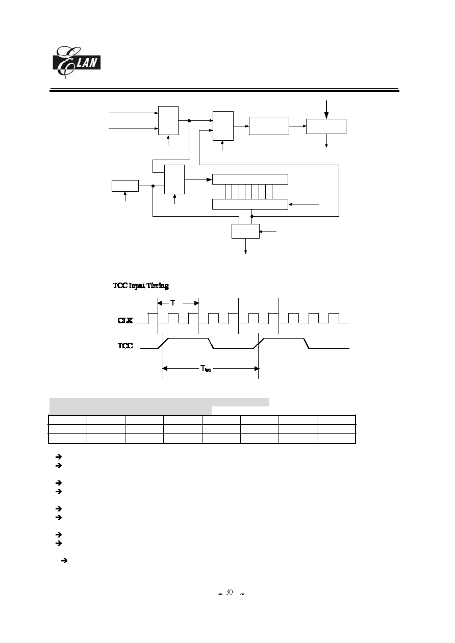
Bit 5(TS): TCC signal source
0
Instruction clock
1
16.384kHz
Instruction clock = MCU clock/2, Refer to RA Bit 4 ~ Bit 6 for PLL and Main clock selection. See fg.17.
Bit 6(INT): INT enable flag
0
interrupt masked by DISI or hardware interrupt
1
interrupt enabled by ENI/RETI instructions
Bit 7(INT_EDGE): interrupt edge type of P77
0
77 's interruption source is a rising edge signal and falling edge signal.
1
P77 's interruption source is a falling edge signal.
CONT register is readable (CONTR) and writable (CONTW).
TCC and WDT:
There is an 8-bit counter available as prescaler for the TCC or WDT. The prescaler is available for the TCC only or WDT
only at the same time.
An 8 bits counter is available for TCC or WDT determined by the status of the bit 3 (PAB) of the CONT register.
See the prescaler ratio in CONT register.
Fig.16 depicts the circuit diagram of TCC/WDT.
Both TCC and prescaler will be cleared by instructions which write to TCC each time.
The prescaler will be cleared by the WDTC and SLEP instructions, when assigned to WDT mode.
The prescaler will not be cleared by SLEP instructions, when assigned to TCC mode.
EM78P915
8-bit Micro-controller
__________________________________________________________________________________________________________________________________________________________________
* This specification is subject to be changed without notice.
2005/12/21 (V2.0)
Instruction clock
M
U
X
TS
PAB
M
U
X
SYNC
2 cycles
TCC overflow interrupt
Data
Bus
TCC(R1)
PSR0 ~
PSR2
8-bit Counter
8-to-1 MUX
M UX
PAB
WDT timeout
PAB
M
U
X
W DT
WDTE
16.384kHz
Figure 18, TCC/WDT structure
ins
Figure 19, TCC timing
IOC5 (PORT5 I/O control, PORT switch, CDAS, LCD bias, CASPWR)
PAGE 0 (PORT5 I/O control register, PORT switch)
7
6
5
4
3
2
1
0
X
IOC56
IOC55
CASPWR
P9SH
P9SL
P8SH
P8SL
R/W-1
R/W-1
R/W-0
R/W-0
R/W-0
R/W-0
R/W-0
Bit 0 (P8SL): Switch low nibble I/O PORT8 or LCD segment output for share pins SEGxx/P8x pins
0
select normal P80 ~ P83 for low nibble PORT8
1
select SEG64 ~ SEG67 output for LCD SEGMENT output.
Bit 1 (P8SH): Switch high nibble I/O PORT8 or LCD segment output for share pins SEGxx/P8x pins
0
select normal P84 ~ P87 for high nibble PORT8
1
select SEG68 ~ SEG71 output for LCD SEGMENT output.
Bit 2 (P9SL): Switch low nibble I/O PORT9 or LCD segment output for share pins SEGxx/P9x pins
0
select normal P90 ~ P93 for low nibble PORT9
1
select SEG72 ~ SEG75 output for LCD SEGMENT output.
Bit 3 (P9SH): Switch high nibble I/O PORT9 or LCD segment output for share pins SEGxx/P9x pins
0
select normal P94 ~ P97 for high nibble PORT9
1
select SEG76 ~ SEG79 output for LCD SEGMENT output.*Bit 4:general register
Bit 4 (CWPWR): Power control of Call Waiting circuit
1/0
enable circuit /disable circuit
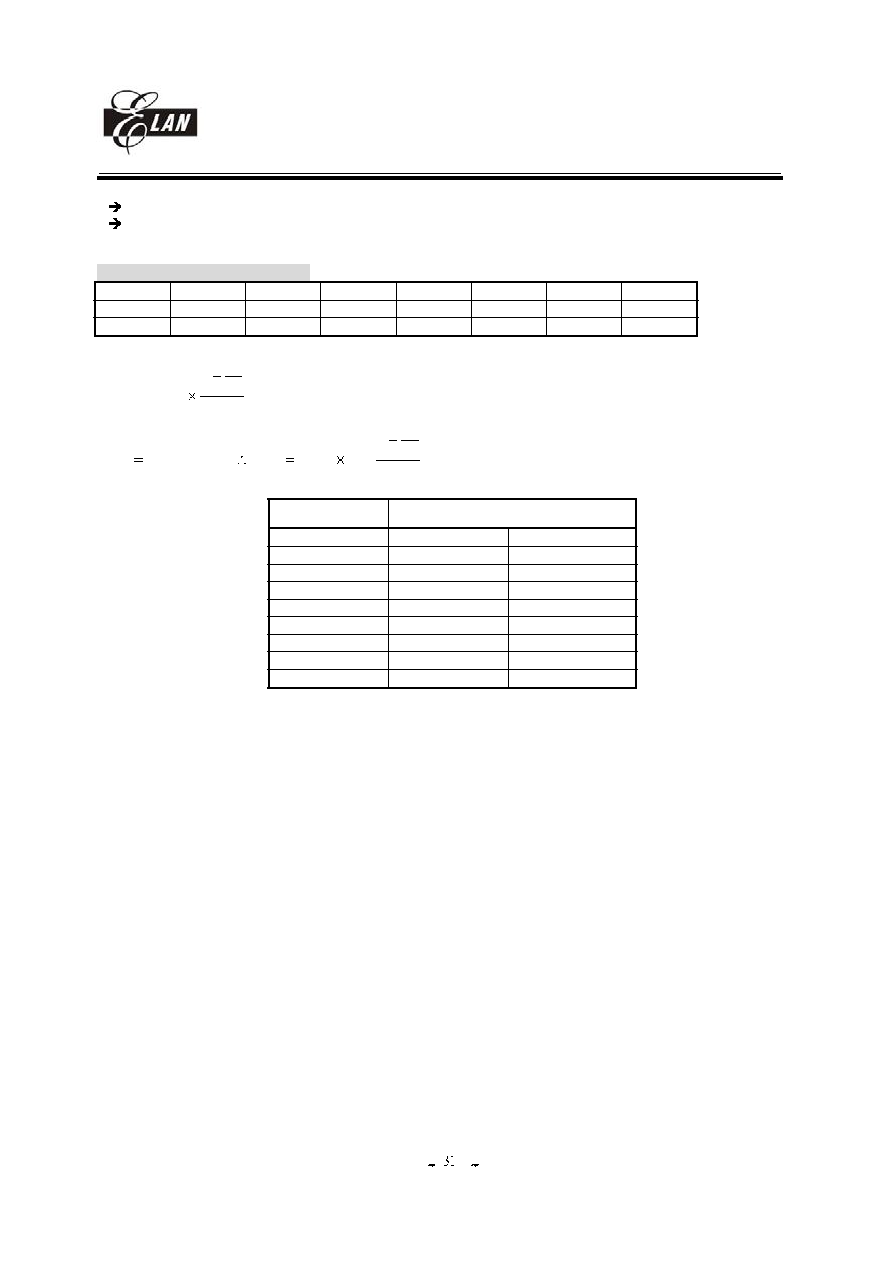
EM78P915
8-bit Micro-controller
__________________________________________________________________________________________________________________________________________________________________
* This specification is subject to be changed without notice.
2005/12/21 (V2.0)
Bit 5~Bit 6(IOC55~IOC56): PORT5 I/O direction control registers.
0
put the relative I/O pin as output
1
put the relative I/O pin into high impedance
Bit 7(Unused)
PAGE 1 (CDAS, LCD bias control)
7
6
5
4
3
2
1
0
X
X
X
CDAS
BIAS3
BIAS2
BIAS1
BIAS0
R/W-0
R/W-0
R/W-0
R/W-0
R/W-0
Bit 0~Bit 3(BIAS0~BIAS3): LCD operation voltage selection
diff
V
=
5
15
5
n
VDD
, n can be set by BIAS0~BIAS3.
diff
LCD
V
VDD
V
,
)
5
15
5
1
(
n
VDD
V
LCD
(BIAS3 to BIAS0)
diff
V
voltage
0000
VDD * (5-0/15)/5
5V
0001
VDD * (5-1/15)/5
4.93V
0010
VDD * (5-2/15)/5
4.86V
0011
VDD * (5-3/15)/5
4.79V
0100
VDD * (5-4/15)/5
4.72V
:
:
:
1101
VDD * (5-13/15)/5 4.14V
1110
VDD * (5-14/15)/5 4.07V
1111
VDD * (5-15/15)/5 4V
Table 15, LCD operation voltage selection
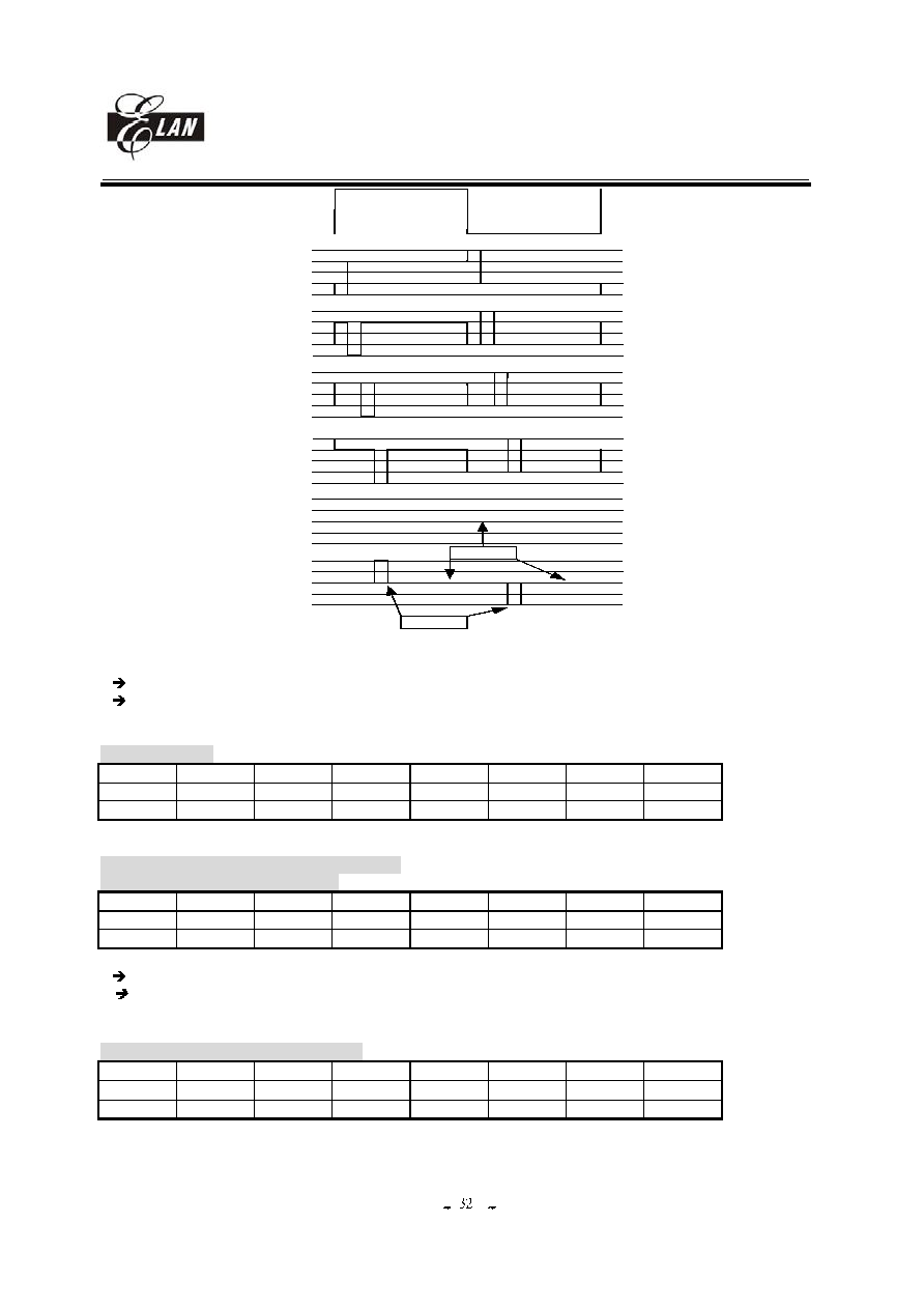
EM78P915
8-bit Micro-controller
__________________________________________________________________________________________________________________________________________________________________
* This specification is subject to be changed without notice.
2005/12/21 (V2.0)
V D D
V 1
V 2
V L C D
F r a m e
C O M 0
C O M 1
C O M 2
C O M 3
S E G
S E G
d a r k
l i g h t
V D D
V 1
V 2
V L C D
V D D
V 1
V 2
V L C D
V D D
V 1
V 2
V L C D
V D D
V 1
V 2
V L C D
V D D
V 1
V 2
V L C D
V 3
V 3
V 3
V 3
V 3
V 3
Figure 20, LCD waveform (1/4 bias) for 1/8 duty, 1/16 duty
Bit 4(CDAS): Current DA switch
0
normal PORT66
1
Current DA output
Bit 5 ~ Bit7 (Unused)
PAGE 2 (Unused)
7
6
5
4
3
2
1
0
X
X
X
X
X
X
X
X
Bit 0 ~ Bit 7 (Unused)
IOC6 (PORT6 I/O control, CDA, PORT switch)
PAGE 0 (PORT6 I/O control register)
7
6
5
4
3
2
1
0
X
IOC66
X
X
IOC63
IOC62
IOC61
IOC60
R/W-1
R/W-1
R/W-1
R/W-1
R/W-1
Bit 0~Bit 3, Bit 6 (IOC60~IOC63, IOC66): PORT60~63, PORT66 I/O direction control register
0
put the relative I/O pin as output
1
put the relative I/O pin into high impedance
Bit 4~5, 7(Unused)
PAGE 1 (Current DA control, DA9~DA3)
7
6
5
4
3
2
1
0
DAEN
DA9
DA8
DA7
DA6
DA5
DA4
DA3
R/W-0
R/W-0
R/W-0
R/W-0
R/W-0
R/W-0
R/W-0
R/W-0
Bit 0~Bit 6(DA0~DA6): Current DA output buffer
User can use this buffer to control the output current of current DA for the driving transistor of speaker.
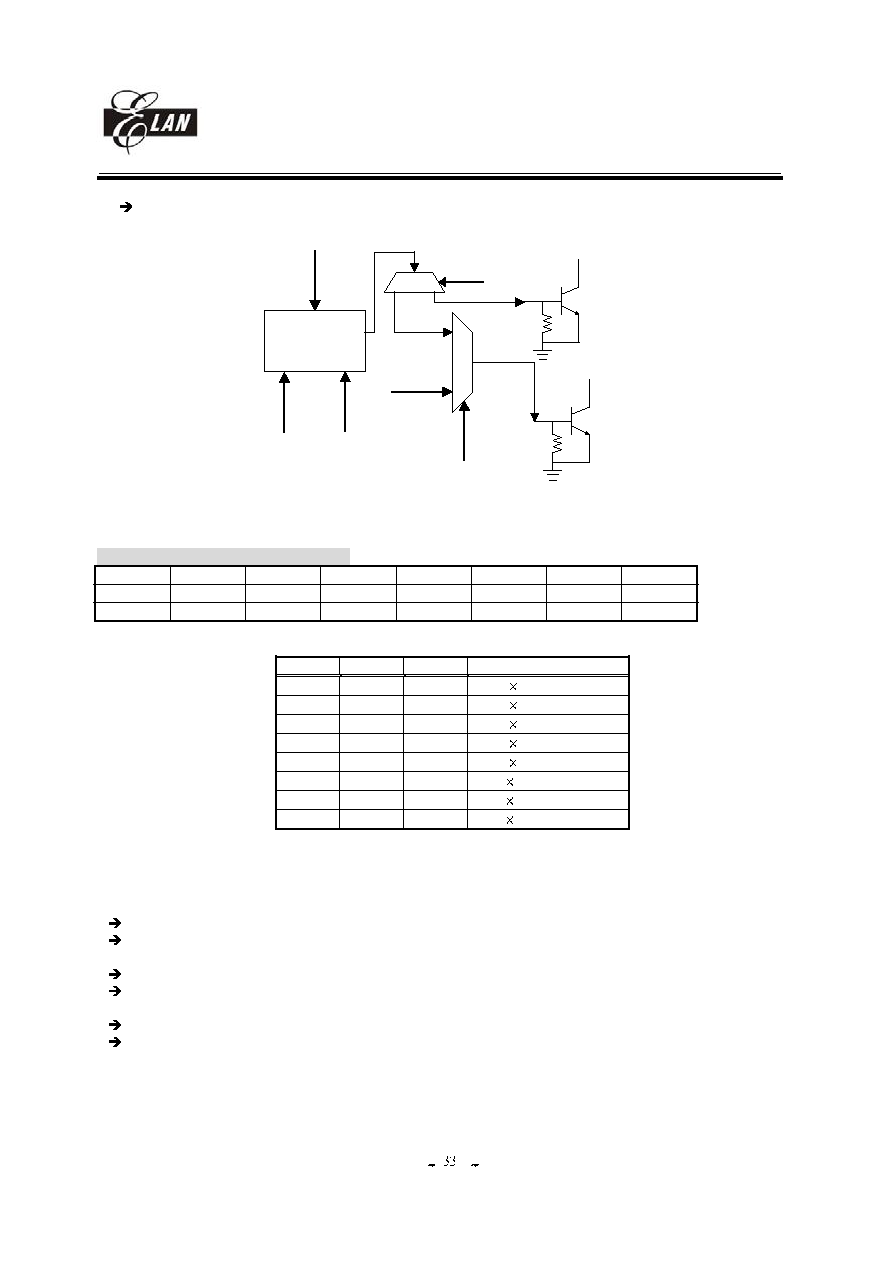
EM78P915
8-bit Micro-controller
__________________________________________________________________________________________________________________________________________________________________
* This specification is subject to be changed without notice.
2005/12/21 (V2.0)
Bit 7 (DAEN): Current DA enable control
0/1
disable/enable
current DA
circuit
DA9~DA0
PORT66
DAS
port66
DA2SW
DAOUTPUT2
VDD
VDD
DAEN
VOL0~3
Figure 21
,
Current DA structure
PAGE 2 (PORT switch, CDAL0~CDAL2)
7
6
5
4
3
2
1
0
PCSH
PCSL
PBS
X
X
CDAL2
CDAL1
CDAL0
R/W-0
R/W-0
R/W-0
R-0
R-0
R/W-0
R/W-0
R/W-0
Bit 0~Bit 2(DAL0~DAL2): change output level of current DA
CDAL2
CDAL1
CDAL0
Output current (mA)
0
0
0
5 1/16 = 0.3125
0
0
1
5 3/16 = 0.9375
0
1
0
5 5/16 = 1.5625
0
1
1
5 7/16 = 2.1875
1
0
0
5 9/16 = 2.8125
1
0
1
5 11/16 = 3.4375
1
1
0
5 13/16 = 4.0625
1
1
1
5 15/16 = 4.6875
Table 16, current DAout1 output level
Bit 3~Bit 4(Unused)
Bit 5(PBS): Switch I/O PORTB or LCD segment output for share pins SEGxx/PBx
0
select normal PB0 ~ PB7 for PORTB
1
select SEG48 ~ SEG55 output for LCD SEGMENT output.
Bit 6(PCSL): Switch low nibble I/O PORTC or LCD segment output for share pins SEGxx/PCx
0
select normal PC0 ~ PC3 for low nibble PORTC
1
select SEG56 ~ SEG59 output for LCD SEGMENT output.
Bit 7(PCSH): Switch high nibble I/O PORTC or LCD segment output for share pins SEGxx/PCx
0
select normal PC4 ~ PC7 for high nibble PORTC
1
select SEG60 ~ SEG63 output for LCD SEGMENT output.

EM78P915
8-bit Micro-controller
__________________________________________________________________________________________________________________________________________________________________
* This specification is subject to be changed without notice.
2005/12/21 (V2.0)
IOC7 (PORT7 I/O control)
PAGE 0 (PORT7 I/O control register)
7
6
5
4
3
2
1
0
IOC77
X
X
X
IOC73
IOC72
IOC71
IOC70
R/W-1
R/W-1
R/W-1
R/W-1
R/W-1
Bit 0~Bit 3, Bit 7(IOC70~IOC73, IOC77): PORT70~73, PORT77 I/O direction control register
0
put the relative I/O pin as output
1
put the relative I/O pin into high impedance
Bit 4~6(Unused)
PAGE 1 (Unused)
7
6
5
4
3
2
1
0
X
X
X
X
X
X
X
X
Bit 0~Bit 7(Unused)
IOC8 (PORT8 I/O control)
PAGE 0 (PORT8 I/O control register)
7
6
5
4
3
2
1
0
IOC87
IOC86
IOC85
IOC84
IOC83
IOC82
IOC81
IOC80
R/W-1
R/W-1
R/W-1
R/W-1
R/W-1
R/W-1
R/W-1
R/W-1
Bit 0~Bit 7(IOC80~IOC87): PORT80~87 I/O direction control register
0
put the relative I/O pin as output
1
put the relative I/O pin into high impedance
PAGE 1 (Unused)
7
6
5
4
3
2
1
0
X
X
X
X
X
X
X
X
Bit 0~Bit 7(Unused)
IOC9 (PORT9 I/O control, DTMF receiver)
PAGE 0 (PORT9 I/O control register)
7
6
5
4
3
2
1
0
IOC97
IOC96
IOC95
IOC94
IOC93
IOC92
IOC91
IOC90
R/W-1
R/W-1
R/W-1
R/W-1
R/W-1
R/W-1
R/W-1
R/W-1
Bit 0~Bit 7(IOC90~IOC97): PORT90~97 I/O direction control register
0
put the relative I/O pin as output
1
put the relative I/O pin into high impedance
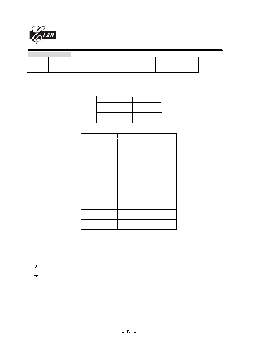
EM78P915
8-bit Micro-controller
__________________________________________________________________________________________________________________________________________________________________
* This specification is subject to be changed without notice.
2005/12/21 (V2.0)
PAGE1 (DTMF receiver)
7
6
5
4
3
2
1
0
DREN
STD
TDP2
TDP1
Q4
Q3
Q2
Q1
R/W-0
R/W-0
R/W-0
R/W-0
R
R
R
R
Bit 0~Bit 3(Q1~Q4): DTMF receiver decoding data
To provide the code corresponding to the last valid tone-pair received (see code table). STD signal which steering
output presents a logic high when a received tone-pair has been registered and the Q4 ~ Q1 output latch updated and
generate a interruption (IOCF has enabled); returns to logic low when the voltage on ST/GT falls below Vtst.
TDP2
TDP1
Tdp
0
0
20 ms
0
1
15 ms
1
0
10 ms
1
1
5 ms
Table 17,Tone detection present time setup
F low
F high
Key
DREN
Q4~Q1
697
1209
1
1
0001
697
1336
2
1
0010
697
1477
3
1
0011
770
1209
4
1
0100
770
1336
5
1
0101
770
1477
6
1
0110
852
1209
7
1
0111
852
1336
8
1
1000
852
1477
9
1
1001
941
1209
0
1
1010
941
1336
*
1
1011
941
1477
#
1
1100
697
1633
A
1
1101
770
1633
B
1
1110
852
1633
C
1
1111
941
1633
D
1
0000
Any
Any
Any
0
xxxx
(x:unknown)
Table 18, DTMF receiver
Bit 4~Bit 5(TDP1, TDP2): we recommend that keep them in [0,0] please.
Bit 6(STD): Delayed steering output.
Presents a logic high when a received tone-pair has been registered and the output latch updated; returns to logic low
when the voltage on St/GT falls below V tst.
0/1 Data invalid/data valid
Bit 7(DREN): DTMF receiver power control
0/1 power down/ power up
Be sure open main clock before using DTMF receiver circuit . A logic low applied to DREN will shut down power of
the device to minimize the power consumption in a standby mode. It stops functions of the filters.
In many situations not requiring independent selection of receive and pause, the simple steering circuit of is applicable.
Component values are chosen according to the following formulae:
t REC = t DP + t GTP t ID = t DA + t GTA
The value of t DP is a parameter of the device and t REC is the minimum signal duration to be recognized by the
receiver. A value for C of 0.1 uF is recommended for most applications, leaving R to be selected by the designer. For
example, a suitable value of R for a t REC of 30mS would be 300k.
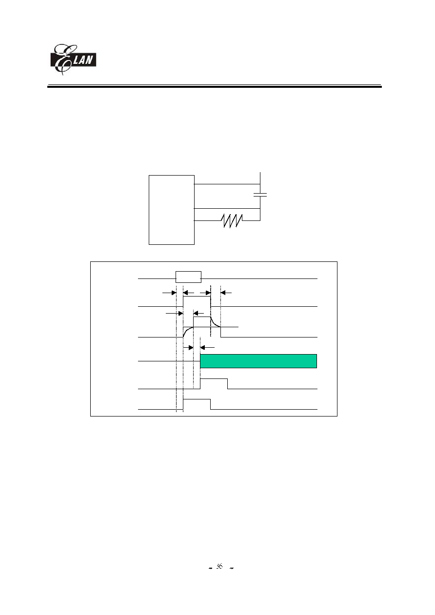
EM78P915
8-bit Micro-controller
__________________________________________________________________________________________________________________________________________________________________
* This specification is subject to be changed without notice.
2005/12/21 (V2.0)
Different steering arrangements may be used to select independently the guard-times for tone-present (t GTP ) and
tone-absent (t GTA ). This may be necessary to meet system specifications which place both accept and reject limits on
both tone duration and inter digital pause.
Guard-time adjustment also allows the designer to tailor system parameters such as talk off and noise immunity.
Increasing t REC improves talk-off performance, since it reduces the probability that tones simulated by speech will
maintain signal condition for long enough to be registered. On the other hand, a relatively short t REC with a long t DO
would be appropriate for extremely noisy environments where fast acquisition time and immunity to drop-outs would be
required.
VDD
ST/GT
EST
VDD
R
C
Figure 22, DTMF receiver delay time control
TONE
TONE
EST
ST/GT
Vtst
1/2 VDD
Q4..Q1
STD
LINE_ENG
Tdp
5~20mS
by S/W
Tgta
30mS Typ.
Tgtp
30mS Typ.
Tpq
8 uS Typ.
Figure 23, DTMF receiver timing
EM78P915
8-bit Micro-controller
__________________________________________________________________________________________________________________________________________________________________
* This specification is subject to be changed without notice.
2005/12/21 (V2.0)
IOCA (CN1's and CN2's clock and scaling, PORT7 pull high control)
PAGE 0 (Counter1's and Counter2's clock and scale setting)
7
6
5
4
3
2
1
0
CNT2S
C2P2
C2P1
C2P0
CNT1S
C1P2
C1P0
C1P1
R/W-0
R/W-0
R/W-0
R/W-0
R/W-0
R/W-0
R/W-0
R/W-0
Bit 0~Bit 2(C1P0~C1P2): Counter1 scaling
C 2
C 1
C
COUNTER1
1P
1P
1P0
0
0
0
1:2
0
0
1
1:4
0
1
0
1:8
0
1
1
1:16
1
0
0
1:32
1
0
1
1:64
1
1
0
1
:128
1
1
1
1
:256
Table 19, counter1 sc ng
Bit 3(CNT1S): Counter1 clock source
0/1 16.384kHz/instruction clock
Bit 4~Bit 6(C2P0~C2P2): Counter2 scaling
C 2
C 1
C
COUNTER2
ali
2P
2P
2P0
0
0
0
1:2
0
0
1
1:4
0
1
0
1:8
0
1
1
1:16
1
0
0
1:32
1
0
1
1:64
1
1
0
1:128
1
1
1
1:256
Table 20, counter2 scaling
Bit 7(CNT2S): Counter2 clock source
lock
0/1 16.384kHz/instruction c
PAGE1 (PORT7 pull high control register)
3
2
1
0
7
6
5
4
PH77
X
X
X
PH73
PH72
PH71
PH70
R/
0
R/
0
R/
0
R/
0
R/
0
W-
W-
W-
W-
W-
Bi
, Bit 7(PH70~PH73, PH77): P
73,
pul
trol
0
e pul
nctio
t 0~Bit 3
ORT70~
PORT 77
l high con
register
disabl
l high fu
n.
1
enable pull high function
Bit 4~6(Unused)
IOCB (PORTB I/O control, PORT6 pull high control)
PAGE 0 (PORTB I/O control register)
7
6
5
4
3
2
1
0
IOCB7
IOCB4
IOCB6
IOCB5
IOCB3
IOCB2
IOCB1
IOCB0
R/W-1
R/W-1
R/W-1
R/W-1
R/W-1
R/W-1
R/W-1
R/W-1
Bit 0~Bit 7(IOCB0~IOCB7) : PORTB(0~7) I/O direction control register
0
put the relative I/O pin as output
high impedance
1
put the relative I/O pin into
EM78P915
8-bit Micro-controller
__________________________________________________________________________________________________________________________________________________________________
* This specification is subject to be changed without notice.
2005/12/21 (V2.0)
PAGE 1 (PORT6 pull high control register)
7
6
5
4
3
2
1
0
X
PH66
PH63
PH62
PH61
PH60
X
X
R/W-0
R/W-0
R/W-0
R/W-0
R/W-0
Bi
, Bit 6 (PH60~PH63, PH66): P
~63,
pul
ntrol
t 0~Bit 3
ORT60
PORT66
l high co
register
0
disable pull high function.
1
enable pull high function
Bit 4~5, 7(Unused)
IOCC (PORTC I/O control, DA0~DA2, DA2SW, VOL0~3)
PAGE 0 (PORT9 I/O control register)
7
6
5
4
3
2
1
0
IOCC7
IOCC6
IOCC5
IOCC4
IOCC3
IOCC2
IOCC1
IOCC0
R/W-1
R/W-1
R/W-1
R/W-1
R/W-1
R/W-1
R/W-1
R/W-1
Bit 0~Bit 7(IOCC0~IOCC7): PORTC (0~7) I/O direction control register
0
put the relative I/O pin as output
1
put the relative I/O pin into high impedance
PAGE 1 (DA0~DA2)
7
6
5
4
3
2
1
0
VOL3
VOL2
VOL1
DA2
1
DA0
VOL0
SW
DA2
DA
R/W-0
R/W-0
R/W-0
R/W
0
R/W-0
R/W-0
-0
R/W-0
R/W-
Bit0~Bit2 (DA0~DA2): Current DA bit0~
Bit 3 (DA2SW): This bit "1"/"0" control DAOUPUT 2 o
T 2 than DAOUTPUT 1 will be
disable, DAOUPUT 2 is turn off than DAOUTPUT will be e
AOUPUT 1).
Bit 4~7 (VOL0~VOL3): There are four bi
ontrol DAo
VOL
L0
M
)
bit2
n/off. If turn on DAOUTPU
nable (assume port66 as D
ts to c
ut2 output volume level.
3 ~ VO
ax voice output current (mA
0000
5 1/16 mA = 0.3125 mA
0001
5 x 2/16 mA = 0.625 mA
0010
5 x 3/16 mA = 0.9375 mA
0011
5 x 4/16 mA = 1.25 mA
0100
5 x 5/16 mA = 1.5625 mA
0101
5 x 6/16 mA = 1.875 mA
0110
5 x 7/16 m
1875 mA
A = 2.
0111
5 x 8/16 mA = 2.5 mA
1000
5 x 9/16 mA = 2.8125 mA
1001
5 x 10/16 mA = 3.125 mA
1010
5 x 11/16 mA = 3.4375 mA
1011
5 x 12/16 mA = 3.75 mA
1100
5 x 13/16 mA = 4.0625 mA
1101
5 x 14/16 mA = 4.375 mA
1110
5 x 15/16 mA = 4.6875 mA
1111
5 mA
Table 21, DAout2 output volume level
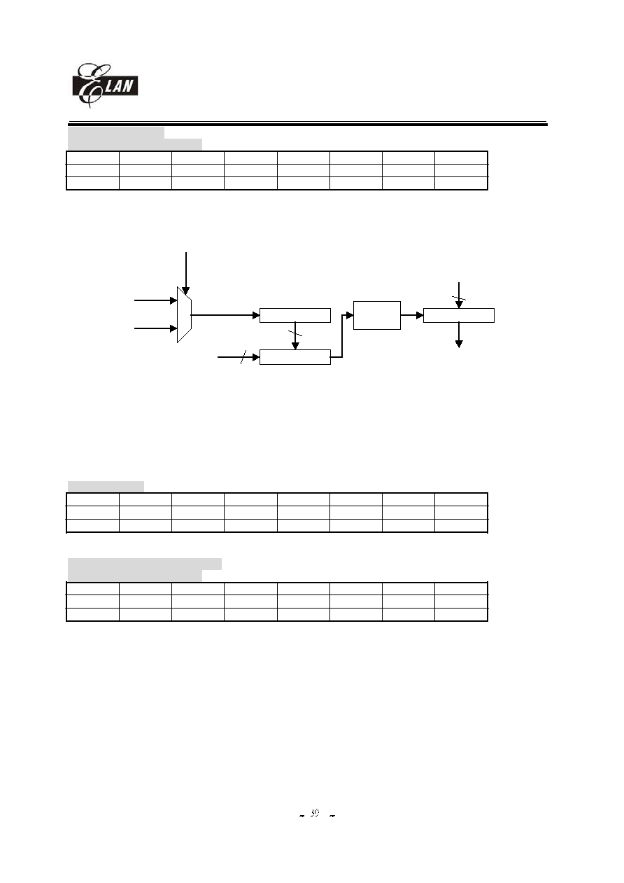
EM78P915
8-bit Micro-controller
__________________________________________________________________________________________________________________________________________________________________
* This specification is subject to be changed without notice.
2005/12/21 (V2.0)
IOCD (Counter1 data)
PAGE 0 (Counter1 data buffer)
7
6
5
4
3
2
1
0
CN17
CN16
CN15
CN14
CN13
CN12
CN11
CN10
R/W-0
R/W-0
R/W-0
R/W-0
R/W-0
R/W-0
R/W-0
R/W-0
Bit 0~Bit 7(CN10~CN17): Counter1's data buffer
User can read and write this buffer. Counter1 is a eight bit up-counter with 8-bit prescaler that user can use IOCD to
preset and read the counter. ( write = preset) After an interruption, it will reload the preset value.
CNT1S
clock
8-bit counter
16.384KHz
MUX
8-1 MU
C1P2~C1P0
X
8-bit
3-bit
sync with
2 cycles
timer 1 buffer
data bus
interrupt
occur
8-bit
Figure 24, counter1 structure
Exa
e:
write:
the data at accumulator to counter1 (preset)
ple:
d write to accumulator
mpl
IOW 0x0D ; write
Exam
read:
IOR 0x0D ;read IOCD data an
PA
nus
GE 1 (U
ed)
7
6
5
4
3
2
1
0
X
X
X
X
X
X
X
X
Bit 0~Bit 7(Unused)
IOCE (Counter2 data, Comparator)
PAGE 0 (Counter2 data buffer)
2
1
0
7
6
5
4
3
CN27
CN26
CN25
CN24
CN23
CN22
CN21
CN20
R/W-0
R/W-0
R/W-0
R/W-0
R/W-0
R/W-0
R/W-0
R/W-0
Bit 0~Bit 7(CN20~CN27): Counter2's data buffer
User can read and write this buffer. Counter2 is a eight bit up-counter with 8-bit prescaler that user can use IOCD to
After a interruption, it will reload the preset value.
IOW
; write the data at accumulator to counter2 (preset)
Exam
:
read:
E data and write to accumulator
preset and read the counter. (write = preset)
Example:
write:
0x0E
ple
IOR 0x0E ;read IOC
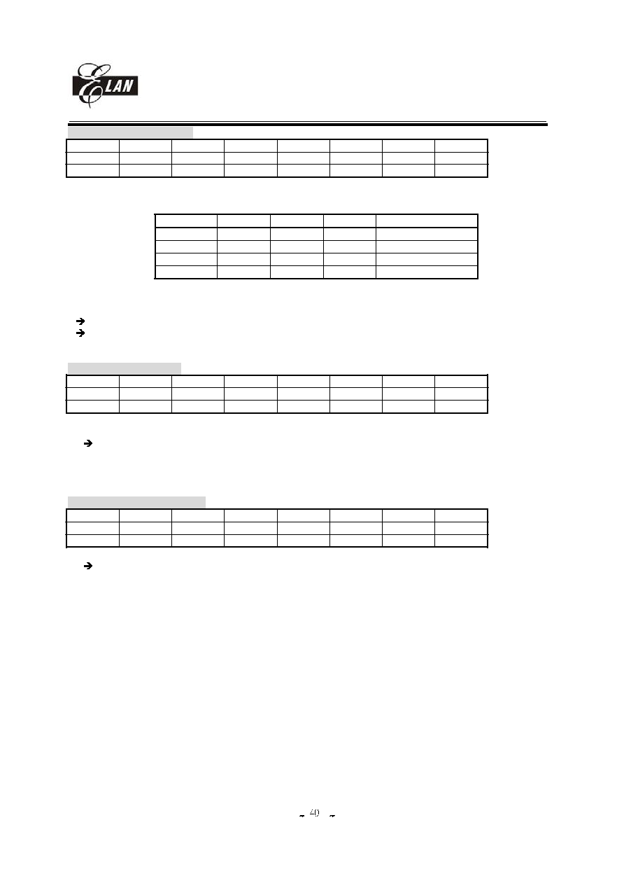
EM78P915
8-bit Micro-controller
__________________________________________________________________________________________________________________________________________________________________
* This specification is subject to be changed without notice.
2005/12/21 (V2.0)
PAGE 1 (Comparator IO set)
7
6
5
4
3
2
1
0
X
X
X
C
IN1
5S2
S1
X
MP
P
P5
X
R/W
-0
-0
R/W-0
R/W
Bit 0 ~ Bit 1(Unused)
Bit 2~Bit 3 (P5S1~P5S2): PORT5 switch
P5S2
P5S1
PORT55
PORT56
Status
0
0
PORT55
PORT56
Normal PORT5 IO
1
1
STGT
EST
DTMF receiver IO
0
1
Unused
1
0
ed
Unus
Table 22, PO
5 switch
parator input.
RT
Bit 4 (CMPIN1): Switch for controlling PORT63 as IO PORT or a com
0
IO PORT63
1
comparator input
Bit 5 ~ Bit 7 (Unused)
PAGE 2 (Energy Detector)
7
6
5
4
3
2
1
0
VRSEL
X
X
X
X
X
X
X
R/
0
W-
B
u
R sel
it for
ator
bit is set to "0", V2_0 ref. circuit will be powered off.
this bit and RD page0 bit 7(CMPEN) are all set to "1".
otice: IOCE page 2 register is a write-only register. To avoid some un-predicted error, please don't read..
it 0 ~ 6(Un sed)
Bi
EL)
ce v
0/1 VR = VDD/VR = 2.0V, When
t 7 (VRS
: Referen
oltage V
ection b
Compar
this
2.0V ref. circuit is only powered on when
N
IOCF (Interrupt Mask Register)
7
6
5
4
3
2
1
0
RBF/STD
FSK/CW
INT2
SDTMI
INT0
CNT2
CNT1
TCIF
R/W-0
R/W-0
R/W-0
R/W-0
R/W-0
R/W-0
R/W-0
R/W-0
Bit 0 ~ Bit 7: Interrupt enable bits.
/1 disable interrupt/enable interrupt
0
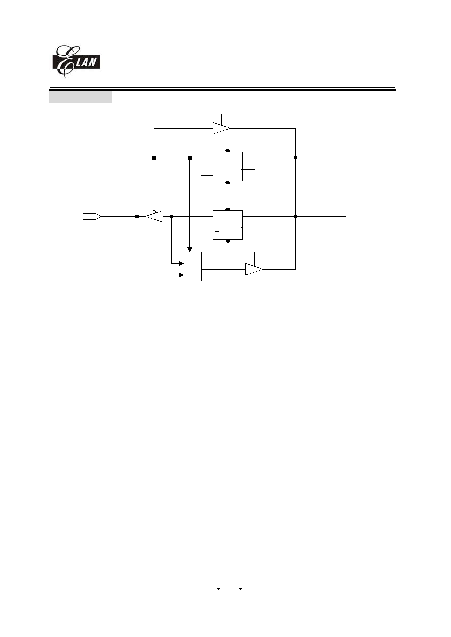
EM78P915
8-bit Micro-controller
__________________________________________________________________________________________________________________________________________________________________
* This specification is subject to be changed without notice.
2005/12/21 (V2.0)
VII. 3 I/O Port
M
U
X
1
0
PDRD
PDWR
CLK
C
L
P
R
D
Q
Q
CLK
C
L
P
R
D
Q
Q
PCWR
IOD
PCRD
PORT
e I/O ports. The I/O ports can be defined as "input" or "output" pins by the
I/O control registers under program control. The I/O registers and I/O control registers are both readable and writable.
The I/O interface circuit is shown in Fig.24
Figure 25, The circuit of I/O port and I/O control register
The I/O registers are bi-directional tri-stat

EM78P915
8-bit Micro-controller
__________________________________________________________________________________________________________________________________________________________________
* This specification is subject to be changed without notice.
2005/12/21 (V2.0)
VII. 4 RESET
The RESET can be caused by
(1) Power on voltage detector reset (POVD) and power on reset
(2) WDT timeout. (if enabled and in GREEN or NORMAL mode)
(3) /RESET pin pull low
At case (1), POVD is controlled by CODE OPTION. If you enable POVD, CPU will reset at 2V under. And
CPU will consume more current about 3uA
<Note>
on reset is a circuit always enable. It will reset CPU
ns are performed.
bits of R4 are cleared.
ounter are cleared.
1"
The other register (bit7 ~ bit0)
address
ter
age0
ter
age1
ister
age0
ister
age1
ister
age2
. And the power
at about 1.4V and consume about 0.5uA.
Once the RESET occurs, the following functio
The oscillator is running, or will be started.
The Program Counter (R2) is set to all "0".
When power on, the upper 3 bits of R3 and the upper 2
The Watchdog timer and prescaler c
The Watchdog timer is disabled.
The CONT register is set to all "
R regis
p
R regis
p
IOC reg
p
IOC reg
p
IOC reg
p
4
00xxxxxx
00000000
5
x0000000
00000000
x1100000
xxx00000
xxxxxxxx
6
x0010000
xxxxxxxx
x1xx1111
00000000
00000000
7
0xxx0000
xxxxxxxx
1xxx1111
xxxxxxxx
8
00000000
xxxxxxxx
11111111
xxxxxxxx
9
00000000
xxxxxxxx
11111111
00000000
A
00000x10
00000000
00000000
0xxx0000
B
00000000
00000000
11111111
x0xx0000
C
00000000
00000000
11111111
00000000
D
0x000000
00000000
00000000
xxxxxxxx
E
1xx00000
x0xx0000
x000xx
0000000
00000000
xx
0
F
00000000
-
-
00000000
Table 24, registers value after reset
Figure 26, Reset timing
EM78P915
8-bit Micro-controller
__________________________________________________________________________________________________________________________________________________________________
* This specification is subject to be changed without notice.
2005/12/21 (V2.0)
VII. 5 wake-up
The controller provided sleep mode for power saving.
(1) SLEEP mode, RA (7)=0 + "SLEP" instruction.
he controller will turn off all the CPU and crystal. Other circu
T
it with power control like key tone control or PLL control
er has to turn it off by software.
mode
ller , and run the program at address zero. The status just like the power on reset. Be sure to
enable circuit at case (1) or (2).
(which has enable register), us
Wake-up from SLEEP
(1) WDT time out
(2) External interrupt
(3) /RESET pull low
All these cases will reset contro
V
ust be cleared in software before leaving the interrupt service routine and
rsive interrupts.
II. 6 Interrupt
RF is the interrupt status register, which records the interrupt request in flag bits. IOCF is the interrupt mask register. TCC
timer, Counter1 and Counter2 are internal interrupt source. P70 ~ P74, P77 (INT0 ~ INT2) are external interrupt input which
interrupt sources are come from the external. If the interrupts are happened by these interrupt sources, then RF register will
generate '1' flag to corresponding register if you enable IOCF register. Global interrupt is enabled by ENI instruction and is
disabled by DISI instruction. When one of the interrupts (when enabled) generated, will cause the next instruction to be
fetched from address 008H. Once in the interrupt service routine the source of the interrupt can be determined by polling the
flag bits in the RF register. The interrupt flag bit m
enabling interrupts to avoid recu
VII. 7 Instruction Set
Instruction set has the following features:
(1) Every bit of any register can be set, cleared, or tested directly.
(2) The I/O register can be regarded as general register. That is, the same instruction can operates on I/O register.
The symbol "R" represents a register designator which specifies which one of the 64 registers (including operational
registers and general purpose registers) is to be utilized by the instruction. Bits 6 and 7 in R4 determine the selected
register bank. "b'' represents a bit field designator which selects the number of the bit, located in the register "R'',
affected b
resen
r 10-bit constant or literal value.
INSTRUCTION
HEX
MNEMONIC
OPERATION
AFFECTED
Instruction
cycle
y the operation. "k'' rep
ts an 8 o
BINARY
STATUS
0 0000 0000 0000
0000
NOP
No Operation
None
1
0 0000 0000 0001
0001
DAA
De
A
cimal Adjust
C
1
0 0000 0000 0010
0002
C
None
1
ONTW
A
CONT
0 0000 0000 0011
0003
SLEP
0
op
T,P
1
WDT, St
oscillator
0 0000 0000 0100
0004
WDTC
0
WDT
T,P
1
0 0000 0000 rrrr
000r
I
OW R
A
IOCR
None
1
0 0000 0001 0000
0010
ENI
Enable Interrupt
None
1
0 0000 0001 0001
0011
DISI
Disable Interrupt
None
1
0 0000 0001 0010
0012
RET
[Top of Stack] PC
None
2
0 0000 0001 0011
0013
RETI
[T
E
t
op of Stack] PC
nable Interrup
None
2
0 0000 0001 0100
0014
CONTR
CONT
A
None
1
0 0000 0001 rrrr
001r
IOR R
IOCR
A
None
1
0 0000 0010 0000
0020
R2+A
,10 do
Z,C,DC
2
TBL
R2 bits 9
not clear
0 0000 01rr rrrr
00rr
M
None
1
OV R,A
A
R
0 0000 1000 0000
0080
CLRA
0
A
Z
1
0 0000 11rr rrrr
00rr
CLR R
0
R
Z
1
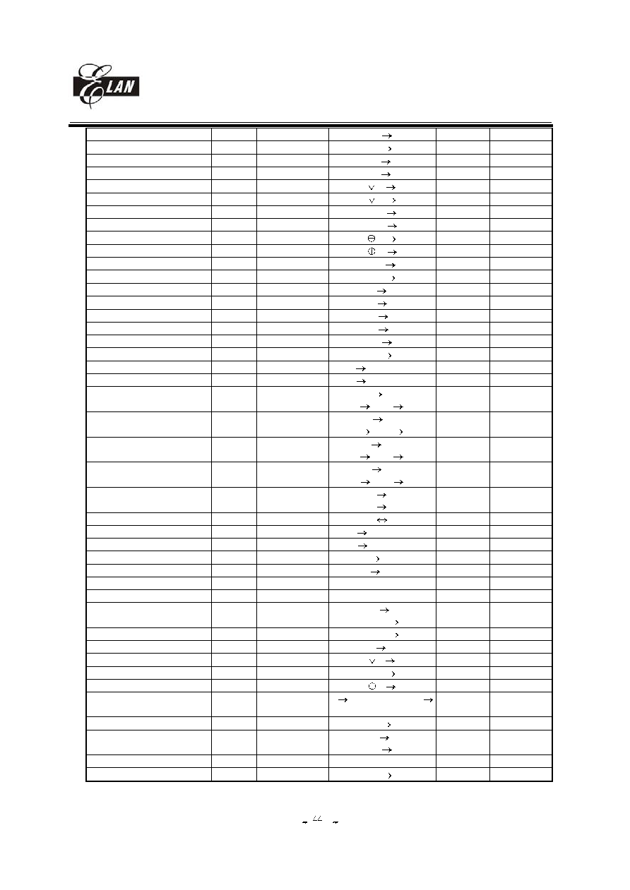
EM78P915
8-bit Micro-controller
__________________________________________________________________________________________________________________________________________________________________
* This specification is subject to be changed without notice.
2005/12/21 (V2.0)
0 0001 00rr rrrr
01rr
SUB A,R
R-A
A
Z,C,DC
1
0 0001 01rr rrrr
01rr
SUB R,A
R-A
R
Z,C,DC
1
0 0001 10rr rrrr
01rr
DECA R
R-1 A
Z
1
0 0001 11rr rrrr
01rr
DEC R
R-1 R
Z
1
0 0010 00rr rrrr
02rr
OR A,R
A R A
Z
1
0 0010 01rr rrrr
02rr
OR R,A
A R R
Z
1
0 0010 10rr rrrr
02rr
AND A,R
A & R A
Z
1
0 0010 11rr rrrr
02rr
AND R,A
A & R R
Z
1
0 0011 00rr rrrr
03rr
XOR A,R
A R A
Z
1
0 0011 01rr rrrr
03rr
XOR R,A
A R R
Z
1
0 0011 10rr rrrr
03rr
ADD A,R
A + R A
Z,C,DC
1
0 0011 11rr rrrr
03rr
ADD R,A
A
Z,C,DC
1
+ R R
0 0100 00rr rrrr
04rr
MOV A,R
R
A
Z
1
0 0100 01rr rrrr
04rr
MOV R,R
R
R
Z
1
0 0100 10rr rrrr
04rr
COMA R
/R
A
Z
1
0 0100 11rr rrrr
04rr
COM R
/R
R
Z
1
0 0101 00rr rrrr
05rr
INCA R
R+1 A
Z
1
0 0101 01rr rrrr
05rr
INC R
R+1 R
Z
1
0 0101 10rr rrrr
05rr
DJZA R
R-1 A, skip if zero
None
2 if skip
0 0101 11rr rrrr
05rr
DJZ R
R-
ro
None
2 if
ip
1 R, skip if ze
sk
0 0110 00rr rrrr
06rr
RRCA R
R(
7)
C
1
R(n) A(n-1)
0) C, C A(
0 0110 01rr rrrr
06rr
RRC R
R(
)
C
1
R(n) R(n-1)
0) C, C R(7
0 0110 10rr rrrr
06rr
RLCA R
R(
)
C
1
R(n) A(n+1)
7) C, C A(0
0 0110 11rr rrrr
06rr
RLC R
R
)
C
1
R(n) R(n+1)
(7) C, C R(0
0 0111 00rr rrrr
07rr
SWAPA R
None
1
R(0-3) A(4-7)
R(4-7) A(0-3)
0 0111 01rr rrrr
07rr
S
WAP R
R(0-3) R(4-7)
None
1
0 0111 10rr rrrr
07rr
JZA R
R+1 A, skip if zero
None
2 if skip
0 0111 11rr rrrr
07rr
JZ R
R+1
zero
2 if
ip
R, skip if
None
sk
0 100b bbrr rrrr
0xxx
BC R,b
0
R(b)
None
1
0 101b bbrr rrrr
0xxx
BS R,b
1
R(b)
None
1
0 110b bbrr rrrr
0xxx
JBC R,b
if R(b)=0, skip
None
2 if skip
0 111b bbrr rrrr
0xxx
JBS R,b
if R(b)=1, skip
None
2 i
ip
f sk
1 00kk kkkk kkkk
1kkk
CALL k
None
2
PC+1
[SP]
(Page, k) PC
1 01kk kkkk kkkk
1kkk
JMP k
(Page, k) PC
None
2
1 1000 kkkk kkkk
18kk
M
None
1
OV A,k
k
A
1 1001 kkkk kkkk
19kk
OR A,k
A k A
Z
1
1 1010 kkkk kkkk
1Akk
AND A,k
A & k A
Z
1
1 1011 kkkk kkkk
1Bkk
XOR A,k
A k A
Z
1
1 1100 kkkk kkkk
1Ckk
RETL k
k
A, [Top of Stack]
None
2
PC
1 1101 kkkk kkkk
1Dkk
SU
k
Z,C,DC
1
B A,
k-A
A
1 1110 0000 0001
1E01
INT
None
1
PC+1
[SP]
001H
PC
1 1110 100k kkkk
1E8k
PAGE k
K->R5(4:0)
None
1
1 1111 kkkk kkkk
1Fkk
ADD A,k
k+A
A
Z,C,DC
1
1 instruction cycle = 2 main clock. Table 25, instructions overview
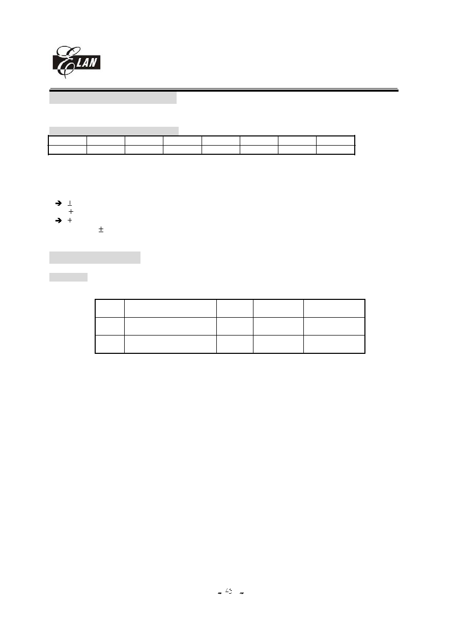
EM78P915
8-bit Micro-controller
__________________________________________________________________________________________________________________________________________________________________
* This specification is subject to be changed without notice.
2005/12/21 (V2.0)
VII. 8 CODE Option Register
The controller has one CODE option register, which is not part of the normal program memory. The option bits
cannot be accessed during normal program execution.
CODE Option Register1 (Program ROM)
7
6
5
4
3
2
1
0
-
-
CWMODE
-
-
-
-
/POT
Bit 0(/POT): program ROM protect option
If set 1 to the bit, program memory can be access; else if clear this bit, program memory can be written only.
Bit 2~4(Unused)
Bit 5(CWMODE): CAS tone (2130 Hz plus 2750 Hz) accepted frequency range deviation select.
0
2% Call waiting accepted frequency range deviation.(Application for China protocol :
1.5% )
1
1.2% Call waiting accepted frequency range deviation.(Application for Europe and USA
protocol :
0.5% )
Bit 6~7(Unused)
VII. 8. 1 PAD Option
PAD Option
Please refer to figure2-1 in page 6. /POVD function will be decided to enable or disable by VDTBL or VDTBH pin.
/POVD
Pin connect
2.2V reset Power on reset
2.0V
sleep mode current
1
VDTBH connect to VDD and
VDTBL floated
No
yes
1uA
0
VDTBL connect to GND and
VDTBH floated
Yes
yes
10uA
Table 26, /POVD
Note: In instruction table, "MOV R, R", R must be the same register.
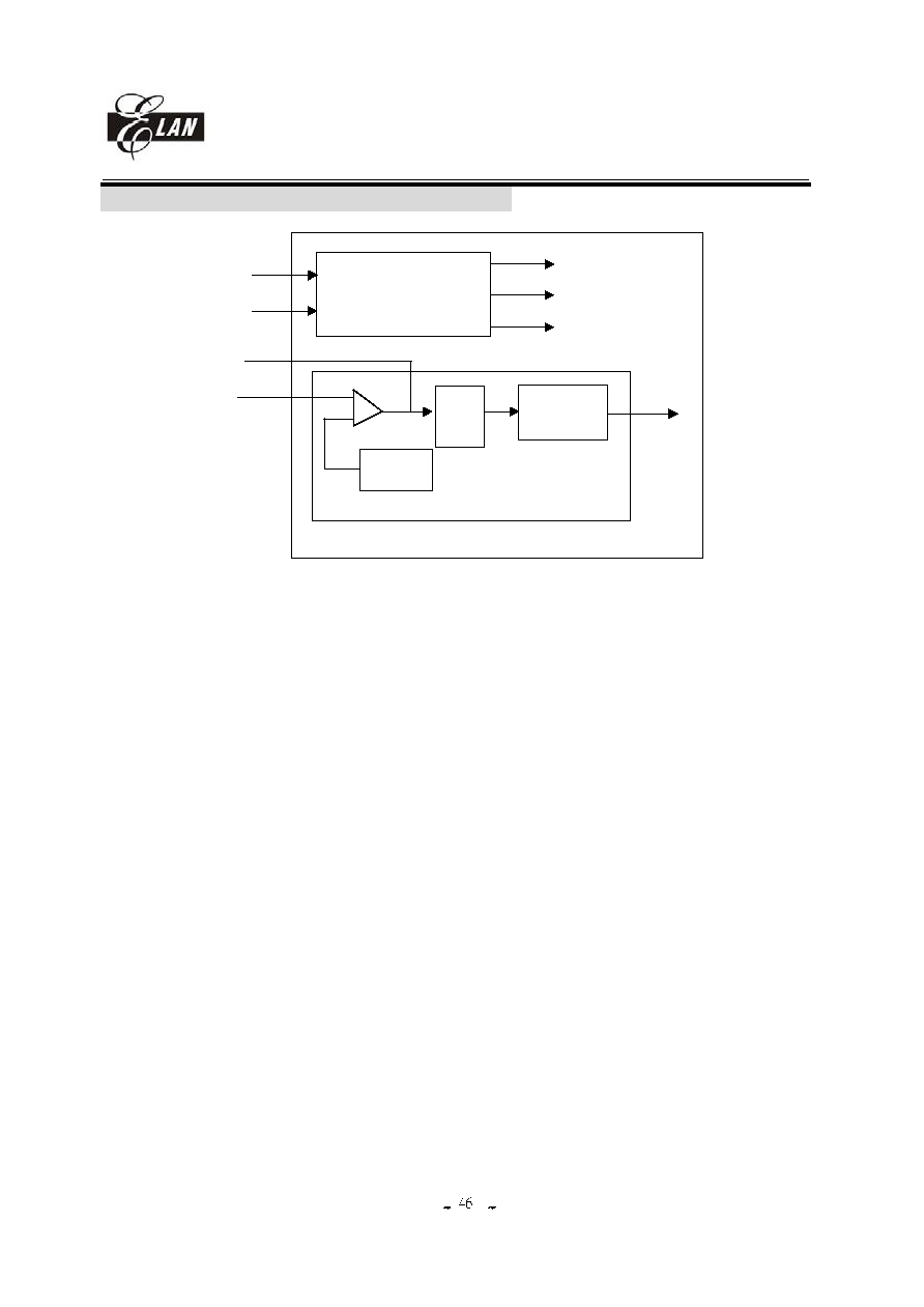
EM78P915
8-bit Micro-controller
__________________________________________________________________________________________________________________________________________________________________
* This specification is subject to be changed without notice.
2005/12/21 (V2.0)
VII. 9 CALL WAITING Function Descriptions
CWTIP
Filter
Vdd/2
Detection
block
Voltage
reference
GAIN
FSK
demodulator
RING
-
+
CAS
TIP
stuttered dail tone
detector
DATA
/CD
/SDT
&
Figure 27, Call Waiting Block Diagram
Call Waiting service works by alerting a customer engaged in a telephone call to a new incoming call. This way the
customer can still receive important calls while engaged in a current call. The CALL WAITING DECODER can detect
CAS(Call-Waiting Alerting Signal 2130Hz plus 2750Hz) and generate a valid signal on the data pins.
The call waiting decoder is designed to support the Caller Number Deliver feature, which is offered by regional Bell
Operating Companies.
In a typical application, after enabling CW circuit (by IOC5 page0 bit4 CWPWR) this IC receives Tip and Ring
signals from twisted pairs. The signals as inputs of pre-amplifier, and the amplifier sends input signal to a band pass
filter. Once the signal is filtered, the Detection block decodes the information and sends it to R3 register bit7 . The
output data made available at R3 CAS bit.
The data is CAS signals. The CAS is normal high. When this IC detects 2130Hz and 2750Hz frequency, then CAS pin
goes to low.
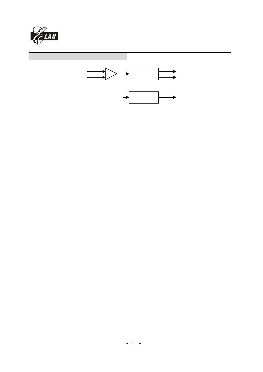
EM78P915
8-bit Micro-controller
__________________________________________________________________________________________________________________________________________________________________
* This specification is subject to be changed without notice.
2005/12/21 (V2.0)
VII. 11 Stuttered dial tone detect (SDT)
FSK block
SDT block
-
+
TIP
RING
FSK Data
/CD
/SDT
Figure 29, SDT block
SDT (Stuttered dial tone) circuit and FSK circuit use the same input OP Amp. When SDTPWR bit (bit 5 of register R6) is
set, SDT circuit is powered on and SDT detection is enabled. SDT detection enable means it is power on and detect 350Hz
plus 440Hz dual frequency. And SDT signal detection output is sent to /SDT bit (bit 4 of register R6) with low enable.
If SDT circuit works, it consists of high-band and low-band pass tone filter, level detect, frequency counting and digital
algorithm to qualify timing.
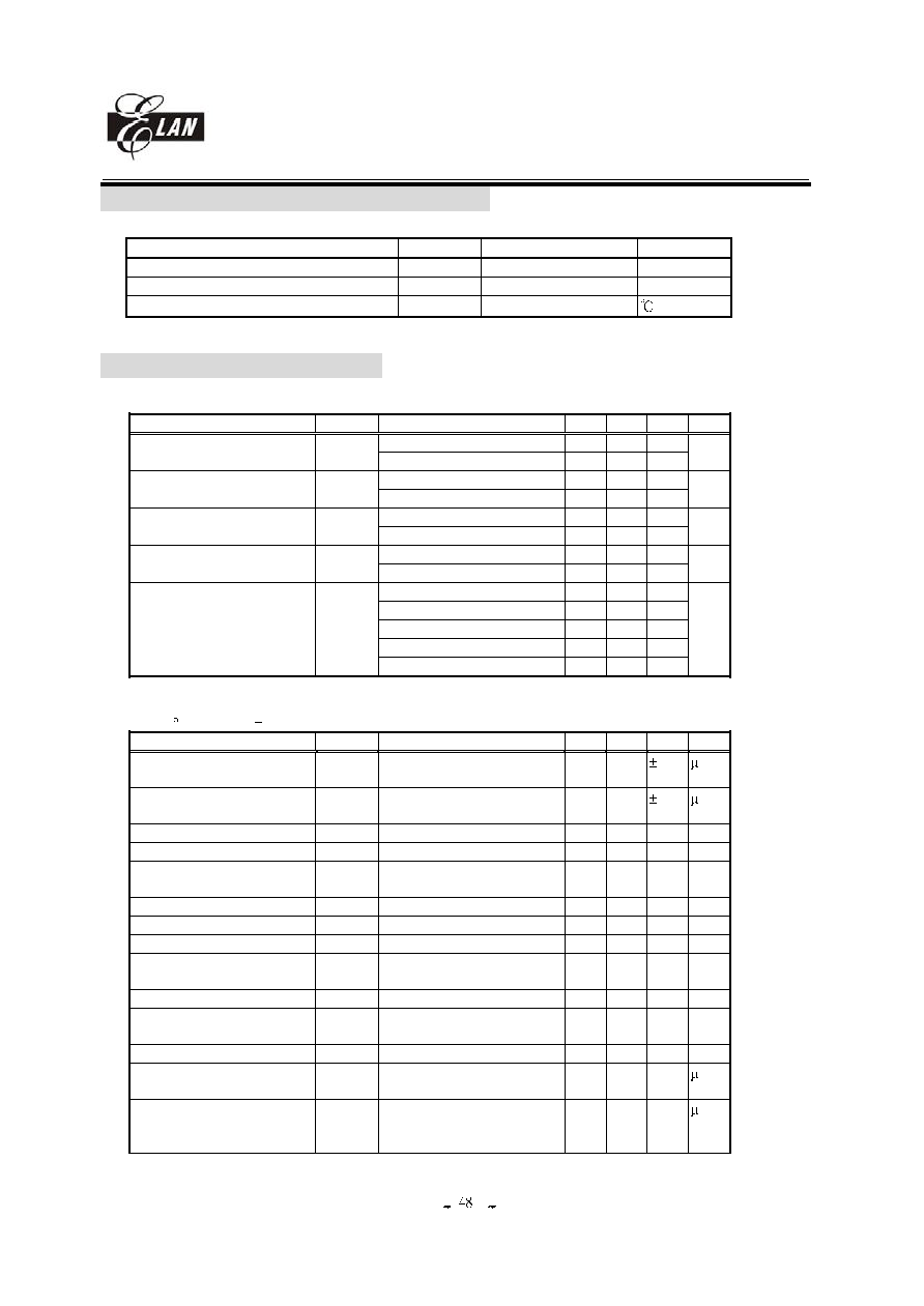
EM78P915
8-bit Micro-controller
__________________________________________________________________________________________________________________________________________________________________
* This specification is subject to be changed without notice.
2005/12/21 (V2.0)
VIII. Absolute Operation Maximum Ratings
RATING
SYMBOL
VALUE
UNIT
DC SUPPLY VOLTAGE
VDD
-0.3 To 6
V
INPUT VOLTAGE
Vin
-0.5 to VDD +0.5
V
OPERATING TEMPERATURE RANGE
Ta
0 to 70
IX. DC Electrical Characteristic
(Operation current consumption for Analog circuit)
Parameter
Symbol
Condition
Min Typ Max Unit
Operation current for FSK
I_FSK
VDD=5V, CID power on
2.5
4.0
mA
VDD=3V, CID power on
2.0
3.5
Operation current for CW
I_CW
VDD=5V, CID power on
2.5
4.0
mA
VDD=5V, CID power on
2.0
3.5
Operation current for DTMF I_DR
VDD=3V, DTMFr power on
2.5
4.0
mA
receiver
VDD=3V, DTMFr power on
2.0
3.5
Current DA output current
I_DA
VDD=5V, CDA power on
2.5
4
mA
VDD=3V, CDA power on
2.0
3.5
Operation current for
I_CMP
VDD=5V, PT power on
0.15 0.3
mA
Comparator
VDD=3V, PT power on
0.13 0.2
SDT
I_SDT
VDD=5V, SDT power on
1.8
3.3
mA
VDD=3V, SDT power on
1.5
3.0
(Ta=25 C, VDD=5V 5%, VSS=0V)
Parameter
Symbol
Condition
Min Typ Max Unit
Input Leakage Current for
input pins
IIL1
VIN = VDD, VSS
1
A
Input Leakage Current for bi-
directional pins
IIL2
VIN = VDD, VSS
1
A
Input High Voltage
VIH
2.0
V
Input Low Voltage
VIL
0.8
V
Input
High
Threshold
Voltage
VIHT
/RESET, TCC, RDET1
2.0
V
Input Low Threshold Voltage VILT
/RESET, TCC,RDET1
0.8
V
Clock Input High Voltage
VIHX
OSCI
1.8
V
Clock Input Low Voltage
VILX
OSCI
1.2
V
Output High Voltage
(port5,8,9,B,C)
VOH1
IOH = -5mA
2.0
V
(port6,7)
IOH = -8mA
2.0
V
Output Low Voltage
(port5,8,9,B,C)
VOL1
IOL = 5mA
0.4
V
(port6,7)
IOL = 8mA
0.4
V
Pull-high current
IPH
Pull-high active input pin at
VSS
-10
-15
A
Power down current
(SLEEP mode)
ISB1
All input and I/O pin at
VDD, output pin floating,
WDT disabled
1
4
A
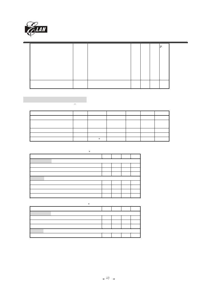
EM78P915
8-bit Micro-controller
__________________________________________________________________________________________________________________________________________________________________
* This specification is subject to be changed without notice.
2005/12/21 (V2.0)
Low clock current
(GREEN mode)
ISB2
CLK=32.768KHz, All analog
circuit disable , All input and
I/O pin at VDD, output pin
floating, WDT disabled, LCD
disable
35
50
A
Operating supply current
(NORMAL mode)
ICC
/RESET=High, PLL enable
CLK=3.579MHz, output pin
floating and LCD enable, all
analog circuit disable
2.8
3.5
mA
Tone generator reference
voltage
Vref2
0.5
0.7
VDD
X. AC Electrical Characteristic
CPU instruction timing (Ta=25 C, VDD=5V, VSS=0V)
Parameter
Symbol Condition
Min
Typ
Max
Unit
Input CLK duty cycle
Dclk
45
50
55
%
Instruction cycle time
Tins
32.768kHz
3.579MHz
60
550
us
ns
Device delay hold time
Tdrh
16
ms
TCC input period
Ttcc
Note 1
(Tins+20)/N
ns
Watchdog timer period
Twdt
Ta = 25 C
16
ms
Note 1: N= selected prescaler ratio.
FSK AC Characteristic (Vdd=5V,Ta=+25 C)
CHARACTERISTIC
Min
Typ
Max Unit
FSK sensitivity
Low Level Sensitivity Tip & Ring @SNR 20dB
-40
-48
dBm
High Level Sensitivity Tip & Ring @SNR 20dB
0
dBm
Signal Reject
-51
dBm
FSK twist
Positive Twist (High Level)
+10
dB
Positive Twist (Low Level)
+10
dB
Negative Twist (High Level)
-6
dB
Negative Twist (Low Level)
-6
dB
CW AC Characteristic (Vdd=5V,Ta=+25 C)
CHARACTERISTIC
Min
Typ
Max Unit
CW sensitivity
Sensitivity @SNR 20dB
-38
dBm
Low Tone Frequency 2130Hz
�1.2
%
High Tone Frequency 2750Hz
�1.2
%
CW twist
Twist
�7
dB
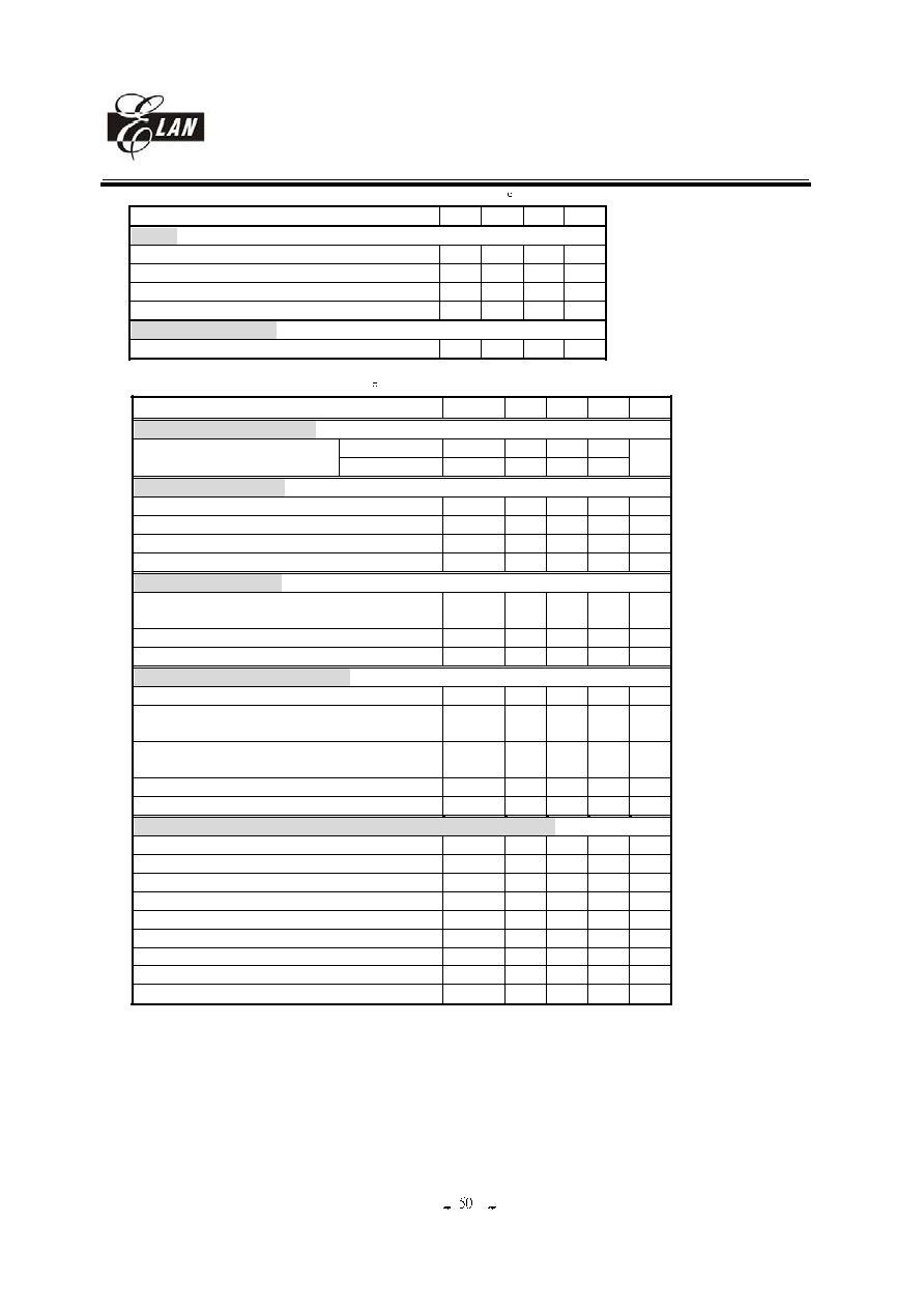
EM78P915
8-bit Micro-controller
__________________________________________________________________________________________________________________________________________________________________
* This specification is subject to be changed without notice.
2005/12/21 (V2.0)
DTMFr (DTMF receiver) AC Characteristic (Vdd=5V,Ta=+25 C)
CHARACTERISTIC
Min
Typ
Max Unit
DTMFr
Low Level Signal Sensitivity
-36
dBm
High Level Signal Sensitivity
0
dBm
Low Tone Frequency
�2
%
High Tone Frequency
�2
%
DTMFr noise endurance
Signal to noise ratio
15
dB
Timing characteristic (Vdd=5V,Ta=+25 C)
Description
Symbol
Min Typ Max Unit
Oscillator timing characteristic
OSC start up
32.768kHz
Tosc
500
ms
3.579MHz PLL
10
FSK timing characteristic
Carrier detect low
Tcdl
--
10
20
ms
Data out to Carrier det low
Tdoc
--
10
20
ns
Power up to FSK(setup time)
Tsup
--
15
20
ms
End of FSK to Carrier Detect high
Tcdh
-
5
ms
CW timing characteristic
CAS input signal length
(2130 ,2750 Hz @ -20dBm )
Tcasi
80
ms
Call waiting data detect delay time
Tcwd
42
ms
Call waiting data release time
Tcwr
26
ms
DTMF receiver timing characteristic
Tone Present Detection Time
Tdp
(ps1)
the guard-times for tone-present
(C=0.1uF, R=300K)
Tgtp
30
ms
the guard-times for tone-absent
(C=0.1uF, R=300K)
Tgta
30
mS
Propagation Delay (St to Q)
Tpq
8
us
Tone Absent Detection Time
Tda
(ps2)
ms
SPI timing characteristic (CPU clock 3.58MHz and Fsco = 3.58Mhz /2)
/SS set-up time
Tcss
560
ns
/SS hold time
Tcsh
250
SCLK high time
Thi
250
ns
SCLK low time
Tlo
250
ns
SCLK rising time
Tr
15
30
ns
SCLK falling time
Tf
15
30
ns
SDI set-up time to the reading edge of SCLK
Tisu
25
ns
SDI hold time to the reading edge of SCLK
Tihd
25
ns
SDO disable time
Tdis
560
ns
(ps1) : Controlled by software
(ps2) : Controlled by RC circuit.

EM78P915
8-bit Micro-controller
__________________________________________________________________________________________________________________________________________________________________
* This specification is subject to be changed without notice.
2005/12/21 (V2.0)
SDT characteristic
Min
Typ
Max
Unit
SDT characteristic
Input sensitivity Tip & Ring pins, VDD=5.0V
-38
dBm
Input frequency tolerance
2.0
%
SDT timing characteristic
SDT signal detect delay time
30
ms
SDT signal release tme
30
ms
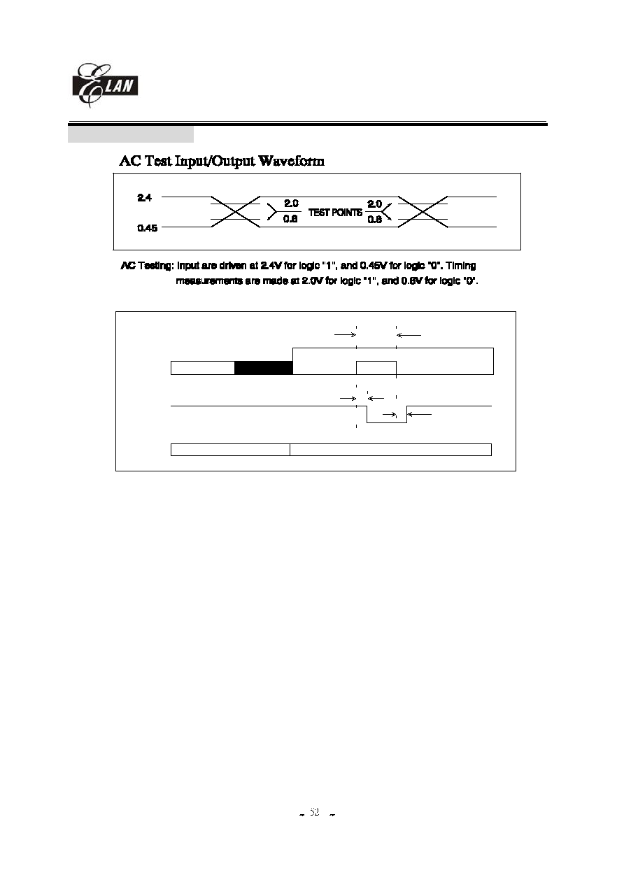
EM78P915
8-bit Micro-controller
__________________________________________________________________________________________________________________________________________________________________
* This specification is subject to be changed without notice.
2005/12/21 (V2.0)
XI. Timing Diagrams
Figure 30, AC test timing
CW PW R
power off
power on
events
Tc w d
p lu g in
o n h o o k
in use
CAS
Tc a s i
CAS
Tc w r
normal
Figure 31, Call waiting timing
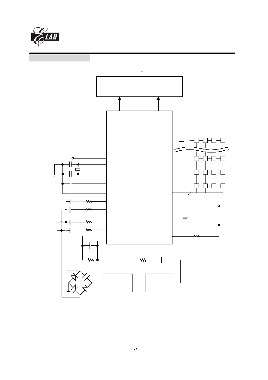
EM78P915
8-bit Micro-controller
__________________________________________________________________________________________________________________________________________________________________
* This specification is subject to be changed without notice.
2005/12/21 (V2.0)
XII. Application Circuit
Using 78P915 build-in LCD driver
P70
SEGx/Px
VDD
XI
N
XOU
T
0.1u
PLL
C
32.768k
27p
27p
AVSS,GN
D
EM78P915
TI
P
RIN
G
4700p
47K
VDD
STG
T
ES
T
Key
matrix
4700p
47K
Line
Interface
Speech
Network
39K
4700p
CWI
N
CWG
S
47p
150K
TI
P
RIN
G
LIN
E
VDD,AVD
D
P71
P72 P73
LCD
pannel
COMMO
N
SEGMEN
T
TES
T
4700p
47K
4700p
47K
EGIN1
EGIN2
SEGx/Px
SEGx/Px
SEGx/Px
Figure 32, Use 78915 build-in LCD driver circuit

EM78P915
8-bit Micro-controller
__________________________________________________________________________________________________________________________________________________________________
* This specification is subject to be changed without notice.
2005/12/21 (V2.0)
XIII. Program Pins location of EM78P915
Port
Name
Note
P70
ACLK
P71
DINCLK
P72
PGMB
P73
OEB
P77
Data I/O
Table 28, program pin location

EM78P915
8-bit Micro-controller
__________________________________________________________________________________________________________________________________________________________________
* This specification is subject to be changed without notice.
2005/12/21 (V2.0)
Appendix
A. Operational/special purpose/code option registers location
Operational register
R 0 ... ... ... ... ... ... ... ... ... ... ... ... ... ... ... ... ... ... ... ... ... ... ... ... ... ... ... ... ... ... ... ... ... ... ... 1 2
R 1 ... ... ... ... ... ... ... ... ... ... ... ... ... ... ... ... ... ... ... ... ... ... ... ... ... ... ... ... ... ... ... ... ... ... ... 1 2
R 2 ... ... ... ... ... ... ... ... ... ... ... ... ... ... ... ... ... ... ... ... ... ... ... ... ... ... ... ... ... ... ... ... ... ... ... 1 2
R 3 ... ... ... ... ... ... ... ... ... ... ... ... ... ... ... ... ... ... ... ... ... ... ... ... ... ... ... ... ... ... ... ... ... ... ... 1 2
R 4 ... ... ... ... ... ... ... ... ... ... ... ... ... ... ... ... ... ... ... ... ... ... ... ... ... ... ... ... ... ... ... ... ... ... ... 1 3
R 5 ... ... ... ... ... ... ... ... ... ... ... ... ... ... ... ... ... ... ... ... ... ... ... ... ... ... ... ... ... ... ... ... ... ... ... 1 6
R 6 ... ... ... ... ... ... ... ... ... ... ... ... ... ... ... ... ... ... ... ... ... ... ... ... ... ... ... ... ... ... ... ... ... ... ... 1 7
R 7 ... ... ... ... ... ... ... ... ... ... ... ... ... ... ... ... ... ... ... ... ... ... ... ... ... ... ... ... ... ... ... ... ... ... ... 1 7
R 8 ... ... ... ... ... ... ... ... ... ... ... ... ... ... ... ... ... ... ... ... ... ... ... ... ... ... ... ... ... ... ... ... ... ... ... 1 7
R 9 ... ... ... ... ... ... ... ... ... ... ... ... ... ... ... ... ... ... ... ... ... ... ... ... ... ... ... ... ... ... ... ... ... ... ... 1 8
R A ... ... ... ... ... ... ... ... ... ... ... ... ... ... ... ... ... ... ... ... ... ... ... ... ... ... ... ... ... ... ... ... ... ... ... 1 8
R B ... ... ... ... ... ... ... ... ... ... ... ... ... ... ... ... ... ... ... ... ... ... ... ... ... ... ... ... ... ... ... ... ... ... ... 2 1
R C ... ... ... ... ... ... ... ... ... ... ... ... ... ... ... ... ... ... ... ... ... ... ... ... ... ... ... ... ... ... ... ... ... ... ... 2 2
R D ... ... ... ... ... ... ... ... ... ... ... ... ... ... ... ... ... ... ... ... ... ... ... ... ... ... ... ... ... ... ... ... ... ... ... 2 2
R E ... ... ... ... ... ... ... ... ... ... ... ... ... ... ... ... ... ... ... ... ... ... ... ... ... ... ... ... ... ... ... ... ... ... ... 2 4
R F ... ... ... ... ... ... ... ... ... ... ... ... ... ... ... ... ... ... ... ... ... ... ... ... ... ... ... ... ... ... ... ... ... ... ... 2 6
Special purpose registers
CO N T...... ... ...... ...... ...... ...... ... ...... ...... ... ...... ...... ...... ... ...... ...... ...... ... ...... ...... 2 8
I O C 5 ... ... ... ... ... ... ... ... ... ... ... ... ... ... ... ... ... ... ... ... ... ...... ... ... ... ... ... ... ... ... ... ... ... ... 2 9
I O C 6 ... ... ... ... ... ... ... ... ... ... ... ... ... ... ... ... ... ... ... ... ... ...... ... ... ... ... ... ... ... ... ... ... ... ... 3 1
I O C 7 ... ... ... ... ... ... ... ... ... ... ... ... ... ... ... ... ... ... ... ... ... ...... ... ... ... ... ... ... ... ... ... ... ... ... 3 3
I O C 8 ... ... ... ... ... ... ... ... ... ... ... ... ... ... ... ... ... ... ... ... ... ...... ... ... ... ... ... ... ... ... ... ... ... ... 3 3
I O C 9 ... ... ... ... ... ... ... ... ... ... ... ... ... ... ... ... ... ... ... ... ... ...... ... ... ... ... ... ... ... ... ... ... ... ... 3 3
I O CA ... ... ... ... ... ... ...... ... ... ... ...... ... ... ... ... ... ... ...... ... ... ... ... ... ...... ... ... ... ...... ... ... 3 6
I O C B... ... ... ... ... ... ... ... ...... ... ... ... ... ... ... ... ...... ... ... ... ... ... ... ... ...... ... ... ... ... ... ... ... 3 6
I O C C... ... ... ... ... ... ... ... ...... ... ... ... ... ... ... ... ...... ... ... ... ... ... ... ... ...... ... ... ... ... ... ... ... 3 7
IO CD ...... ...... ...... ...... ...... ...... ...... ......... ...... ...... ...... ...... ...... ...... ...... ...... ...... .38
I O C E... ... ... ... ... ... ... ... ... ... ... ... ... ... ...... ... ... ... ... ... ... ... ... ... ... ... ... ... ... ... ...... ... ... 3 8
I O C F... ... ... ... ... ... ... ... ... ... ... ... ... ... ... ... ... ... ... ... ... ... ... ... ... ... ... ... ... ... ... ... ... ... ... 4 0
Code option registers
Code option register1...................................................................................................45
PAD option register1...................................................................................................45

EM78P915
8-bit Micro-controller
__________________________________________________________________________________________________________________________________________________________________
* This specification is subject to be changed without notice.
2005/12/21 (V2.0)
B. Figure/table list
Figure list
Figure 1, Register overview description..............................................................................2
Figure 2, Pin assignment................................................................................................6
Figure 3, Block diagram.............................................................................................7
Figure 4, operational registers overview...........................................................................10
Figure 5, Special purpose registers overview........................................................................10
Figure 6, general purpose registers 10 ~ 1F........................................................................11
Figure 7, general purpose registers 20 ~ 3F in Bank0/1/2/3......................................................11
Figure 8, program counter organization..............................................................................12
Figure 9, Single SPI Master / Salve Communication............................................................14
Figure 10, SPI structure................................................................................................15
Figure 11, SPI timing...................................................................................................16
Figure 12, the relation between bit 1 ~ bit 3 of FSK in RA.........................................................19
Figure 13, the relation between 32.768kHz and PLL...............................................................20
Figure 14, Comparator timing..........................................................................................23
Figure 15, Comparator circuit..........................................................................................23
Figure 16, key scan waveform for 1/8, 1/16 duty...............................................................25
Figure 17, KEYSCAN and segments..............................................................................25
Figure 18, TCC/WDT structure.........................................................................................29
Figure 19, TCC timing...................................................................................................29
Figure 20, LCD waveform (1/4 bias) for 1/8 duty, 1/16 duty.............................................31
Figure 21, Current DA structure.......................................................................................32
Figure 22, DTMF receiver delay time control........................................................................35
Figure 23, DTMF receiver timing......................................................................................35
Figure 24, counter1 structure............................................................................................38
Figure 25, The circuit of I/O port and I/O control register.........................................................41
Figure 26, Reset timing..................................................................................................42
Figure 27, Call Waiting Block Diagram..............................................................................46
Figure 29, SDT block..............................................................................................48
Figure 30, AC test timing................................................................................................52
Figure 31, Call waiting timing..........................................................................................52
Figure 32, Use 78915 build-in LCD driver circuit..................................................................53
Table list
Table 1, initial setting reference in using ICE915.....................................................................2
Table 2, Event for power down bit and timer out bit............................................................13
Table 3, relation with IOCP1S bit and IOCPAGE bit.........................................................13
Table 4, SPI baud rate selection....................................................................................14
Table 5, program page selection....................................................................................16
Table 6, main clock selection.......................................................................................19
Table 7, sleep/green/normal modes with wake up signal......................................................20
Table 8, Common/Segment signal....................................................................................21
Table 9, channel selection of CMP.................................................................................22
Table 10, LCD common mode.......................................................................................24
Table 11, LCD operation function define...........................................................................24
Table 12, relation with Duty mode and COM.....................................................................24
Table 13, interrupt trigger.............................................................................................27
Table 14, pre-scale of TCC and WDT..............................................................................28
Table 15, LCD operation voltage selection........................................................................30
Table 16, current DA output level.................................................................................32
Table 17, DTMF receiver.............................................................................................34
Table 18, Tone detection present time setup.....................................................................34
Table 19, counter1 scaling.............................................................................................36
Table 20, counter2 scaling.............................................................................................36
Table 21, output volume level..........................................................................................37
Table 22, PORT5 switch.............................................................................................39
Table 24, registers value after reset.................................................................................42
EM78P915
8-bit Micro-controller
Table 25, instructions overview.......................................................................................44
__________________________________________________________________________________________________________________________________________________________________
* This specification is subject to be changed without notice.
2005/12/21 (V2.0)
Table 26, /POVD........................................................................................................45
Table 28, program pin location....................................................................................54
C. EM78P915/915 family list
Type
OTP
OTP
OTP
OTP
Note
Product NO.
P915/915
P914/914
P916/916
P880/880
Kernel
Operation voltage
2.2V ~ 5.5V
2.2V ~ 5.5V
2.2V ~ 5.5V
2.2V ~ 5.5V
Operation clock
MAX
10.74MHz
10.74MHz
10.74MHz
10.74MHz
Program ROM size
32K*13
32K*13
32K*13
32K*13
8-bit WDT*1
8-bit TCC*1
Internal INT*3
Internal INT*3
Internal INT*3
Internal INT*3
Interruption
External INT*7
External INT*5
External INT*7
External INT*3
Stack level
8
8
8
8
Counter
8-bit CNT*2
8-bit CNT*2
8-bit CNT*2
8-bit CNT*2
Data RAM size
2.5K*8
2.5K*8
2.5K*8
2.5K*8
Idle mode
Sleep mode
I/O Port
MAX
44 bi-direction
44 bi-direction
44 bi-direction
44 bi-direction
/POVD level
2.2V
2.2V
2.2V
2.2V
POR level
2.0V
2.0V
2.0V
2.0V
Digital IP circuit
SPI
10-bit CDA
Analog IP circuit
LCD
LCD pin number
COM: 16
SEG: 60
COM: 16
SEG: 60
COM: 16
SEG: 60
Bias: 1/4
Bias: 1/4
Bias: 1/4
LCD bias and duty
Duty: 1/8, 1/16
Duty: 1/8, 1/16
Duty: 1/8, 1/16
Call waiting
FSK decode
DTMF receiver
DED
SDT decode
Comparator
Note: symbol " " is represent the function existed. If the space is empty, the function is disabled or un-existed.
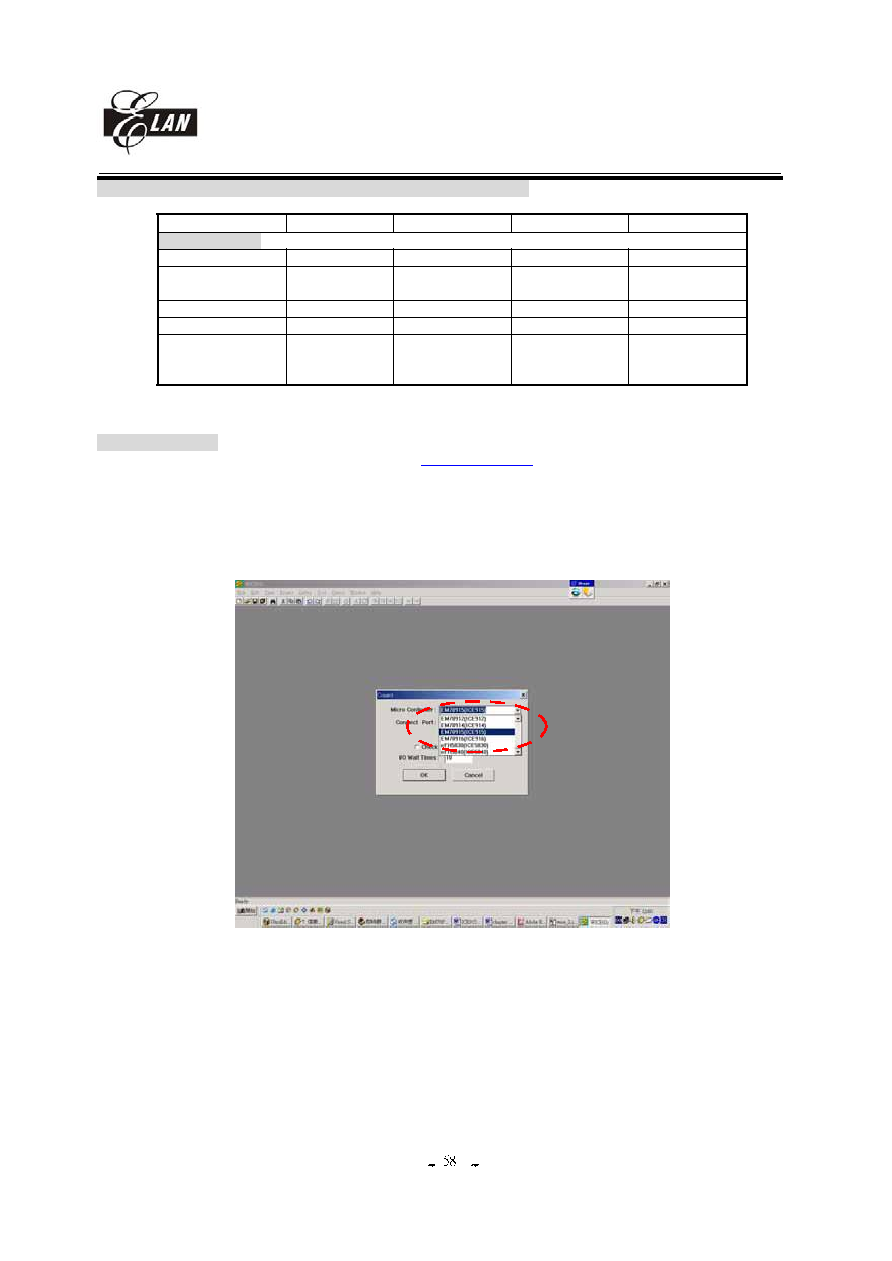
EM78P915
8-bit Micro-controller
__________________________________________________________________________________________________________________________________________________________________
* This specification is subject to be changed without notice.
2005/12/21 (V2.0)
D. Development tool and reference document for EM78P915/915 family
Product (OTP/Mask) NO.
P915/915
P914/914
P916/916
P880/880
Development tool
ICE (ROM-Less) NO.
ICE915
ICE915
ICE915
ICE915
WICE version
2.993-051004 or
above
2.993-051004 or
above
2.993-051004 or
above
2.993-051004 or
above
Writer S/W version
3.1 or above
3.1 or above
3.1 or above
3.1 or above
Writer H/W version
3.1 or above
3.1 or above
3.1 or above
3.1 or above
Reference document
Chapter 2 of
ICE915 family
user guide
Chapter 3 of
ICE915 family user
guide
Chapter 4 of
ICE915 family user
guide
Chapter 5 of
ICE915 family user
guide
Note: if users want to develop products by using P915/915, these tools such as ICE915, WICE, reference
documents and Writer are necessary tools for developing and debugging level.
E. ICE915 in WICE
Step1: Download WICE steup.exe file from our web site
www.emc.com.tw
Step2: Setup WICE. (In this description, we only introduce about ICE915 in WICE, but more detail about WICE using, users
have to refer to WICE manual please)
Step3: Choice your ICE NO. (ICE915, ICE914, ICE916 or ICE880) and press "OK" button after executed WICE. If users
can't find ICE NO. Please presses "Cancel" and refer to step4 to check WICE version.
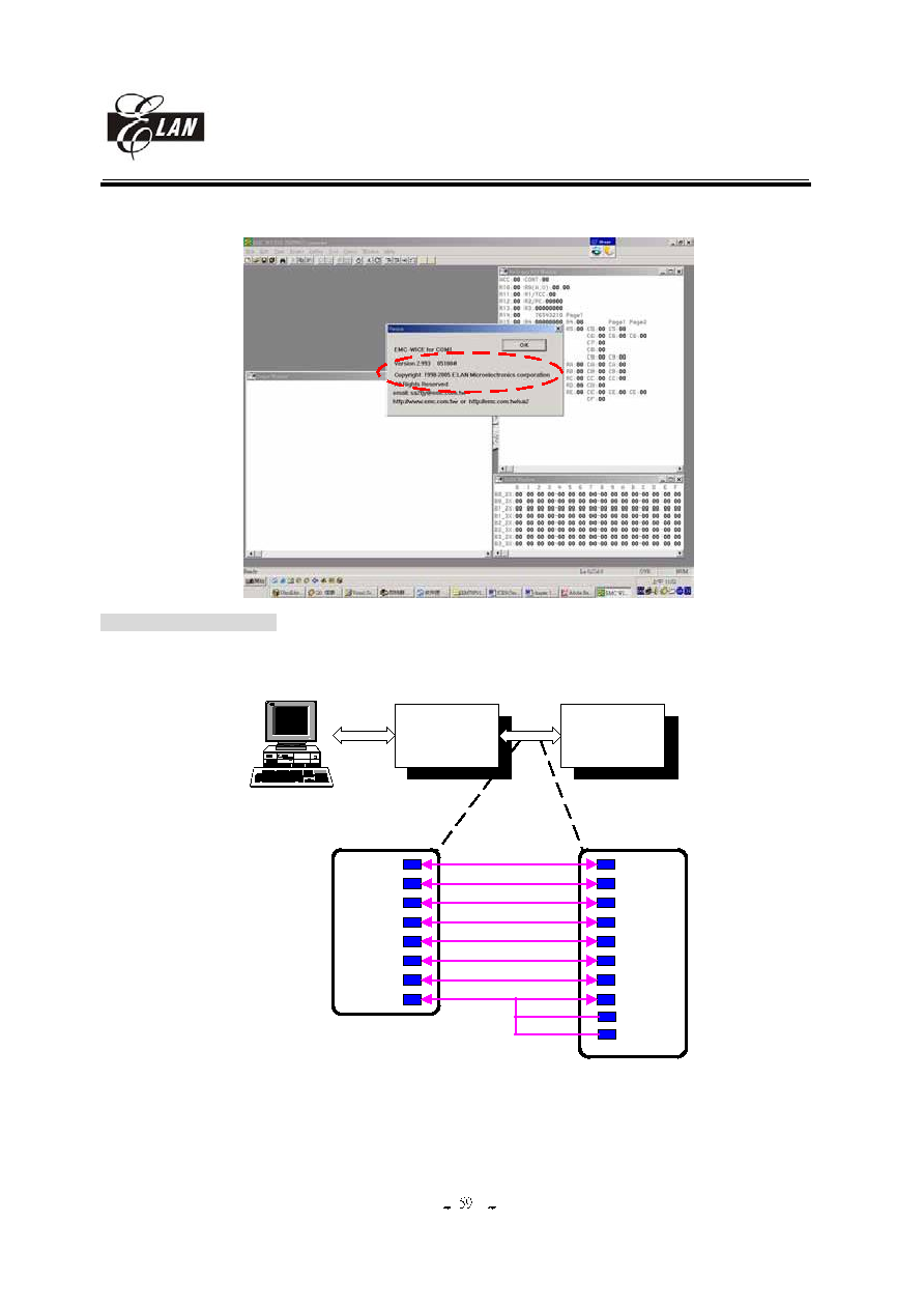
EM78P915
8-bit Micro-controller
__________________________________________________________________________________________________________________________________________________________________
* This specification is subject to be changed without notice.
2005/12/21 (V2.0)
Step4: Check WICE version after installed, the number must be 2.993-051004 or above. If version is older than this number,
please update your WICE.
F. Program EM78P915 note
Step1: Please check your tools. It has to include WTRFI S/W and WTRFI H/W. And remember to confirm their version first.
Step2: The connection between WTRFI H/W, PC, EM78P915
WTRFI H/W
EM78P915
Printer Port
Program Pin
VDD
VPP
DINCLK
ACLK
PGMB
OEB
DATA
GND
P70
P71
P72
P73
P77
GND
VDD
Reset
WTRFI H/W
EM78P915
TEST1
XIN
Step3: After executed WTRFI S/W and choice 915, users can write/read code from EM78P915. More detail description about
WTRFI S/W and H/W, users can refer to WTRFI manual.