 | –≠–ª–µ–∫—Ç—Ä–æ–Ω–Ω—ã–π –∫–æ–º–ø–æ–Ω–µ–Ω—Ç: EM91710A | –°–∫–∞—á–∞—Ç—å:  PDF PDF  ZIP ZIP |

1
EM91710A/B
TONE/PULES SWITCHABLE DIALER
* This specification are subject to be changed without notice.
9.30.1997
GENERAL DESCRIPTION
The EM91710A/B are Tone/Pulse switchable dialer which are fabricated in CMOS technology with wide
operating voltage for both tone and pulse mode, and consumes very low memory retention current in ON-HOOK
state.
FEATURES
∑ Tone/pulse switchable dialer.
∑ One 32-digit last number redial memory.
∑ Pulse to tone (P
T) is provided for PBX operation.
∑ Flash key is available.
∑ Minimum tone duration is 98ms or 83ms.
∑ Minimum intertone pause is 98ms or 83ms.
∑ Uses 3.579545 MHz crystal or ceramic resonator.
∑ Many options can be selected.
Mode (10 PPS ; 20 PPS ; Tone)
M/B ratio (40 : 60 ; 33 : 66)
Pause time (3.6s)
∑ Flash function (RESET)
P
T pause time (3.6s)
Flash time (600ms; 300ms; 100ms; or 80ms).
∑ Mixed dialing.
∑ Handfree function is provided for speaker phone application.
∑ Power on reset circuit is provided.
∑ Package in DIP18 or DIP16.
PIN ASSIGNMENTS
EM91710A/B
TONE/PULSE SWITCHABLE DIALER
C2
C3
C4
C1
OSCI
OSCO
XMUTE
V
16
15
14
13
12
11
10
9
1
2
3
4
5
6
7
8
EM91710A
R3
R2
R1
R4
TONE
PO
HKS
V
DD
SS
C2
C3
C4
C1
OSCI
OSCO
XMUTE
HFI
18
17
16
15
14
13
12
11
10
1
2
3
4
5
6
7
8
9
EM91710B
SS
V
DD
R3
R2
R1
R4
TONE
PO
HKS
V
HFO
* This specification are subject to be changed without notice.
EM91710A/B
TONE/PULSE SWITCHABLE DIALER
2
9.30.1997
KEYBOARD ASSIGNMENT
C1
C2
C3
C4
R1
1
2
3
P
T
R2
4
5
6
F
R3
7
8
9
P
R4
*or*/T
0
#
RD
1). P
T : In pulse mode, execute P
T function.
2). F
: Flash key.
3). RD
: Redial key.
4). P
: Pause key.
5). */T
: In pulse mode, execte P
T function
In tone mode, execte "*" key.
FUNCTIONAL BLOCK DIAGRAM
DIALING SIGNAL OPTION :
(820K
typically)
R
NR
R
R
NR
NR
NR
R
Row3 Row4 flash time(ms)
600
300
100
80
a]:Flash time:
Note: NR:no resistance.
R : A resistance connect to Vss
UR: A resistance connect to V
DD
MODE
PULSE RATE
M/B
R
NR
TONE
R
R
TONE
NR
NR
PULSE
20PPS
40:60
NR
R
PULSE
20PPS
33:66
UR
NR
PULSE
10PPS
40:60
UR
R
PULSE
10PPS
33:66
Row1 Row2
b).
c]:Tone function:
Tone Duration
inter-Tone
Pause
NR
R
98 ms
83 ms
98 ms
83 ms
Col1
*
R
*/T
NR
Col2
*or*/T
select
d]:Key type select
ROW2
OSC.
COLUMN
INTERFACE CKT.
DIVIDER
KERNEL CONTROL CKT.
ROW/COLUMN
PROGRAMMING
COUNTER
ROW
INTERFACE CKT.
LNB MEMORY
DECODER &
DATA LATCH
PULSE
GENERATOR
D/A CONVERTER
INPUT INTERFACE CKT.
OUTPUT INTERFACE CKT.
COL1
COL2
COL3
COL4
OSCI
OSCO
ROW1
ROW3
ROW4
HKS
HFI
V
SS
TONE
PO
XMUTE
HFO
V DD
3
EM91710A/B
TONE/PULES SWITCHABLE DIALER
* This specification are subject to be changed without notice.
9.30.1997
PIN DESCRIPTION
Symbol
Function
C1
C2
C3
C4
R1
R2
R3
R4
OSCI
OSCO
XMUTE
V
SS
V
DD
HKS
PO
Figure 1a : Single contact form keyboard configuration
Row
Column
V
DD
VSS
VDD
VSS
Figure 1b : Dual contact form keyboard configuration
Figure 1c : Electronic signal input keyboard configuration
Row
Column
Row
Column
Provides keyboard scanning .
a. Keyboard scanning:
HKS pin is LOW, the column group stays in "HIGH" stays and row group stays in "LOW" state.
The key pad is compatible with the standard dual contact matrix keyboard (as Figure 1b.), the
inexpensive single contact keyboard (as Figure 1a.), and electronic input (as Figure 1c.).
When HKS is "low", a valid key entry is defined by related Row & Column connection or by
electronic input; (as show in Figure 1c).
Activation of two or more keys will result in no response, except for single key.
To avoid keyboard bouncing error, this chip provides built-in debounce circuit. (The debounce
time = 20 ms.)
Oscillator input & Oscillator output pins.
The 3.579545 MHz oscillator is formed by a built-in inverter inside of this chip and by connecting a
3.579545 MHz crystal or a ceramic resonator across the OSCI and OSCO pins. (built-in feedback
resistor and capacitor)
When HKS is "low", a valid key-in may turn on this oscillator and generates a 3.579545 MHz clock.
Mute output pins.
NMOS open drain output structure.
The output is in "low" state during dialing sequence (both Pulse and Tone mode) otherwise this pin
is "high-impedance" .
Long (continue) Mute.
Negative power supply pin.
Positive power supply pin.
Hook switch input pin.
When the handset is in ON-HOOK state, this pin must be pulled "high" in order to disable the dialing
operation and decrease the power consumption.
When in OFF-HOOK state, the HKS pin must be pulled "low" state for all function operation.
Pulse output signal pin.
NMOS open drain output structure.
The output is "low" during pulse dialing and Flash operation, otherwise this output is "floating".
* This specification are subject to be changed without notice.
EM91710A/B
TONE/PULSE SWITCHABLE DIALER
4
9.30.1997
Symbol
Function
TONE
HFI
HFO
Dual Tone Multi-frequency output pin.
In TONE mode, when a entry of digit key (include * , # key), this pin will sent out a corresponding
DTMF signal.
The TONE pin provides minimum tone duration (t
TD
),& minimum intertone pause time to support rapid
key-in. If key-in time is less than t
TD
, DTMF signal will last for t
TD
, otherwise the tone duration will
last as long as the key is pressed.
Handfree input control pin.
Toggle input sturcture, falling edge trigger.
It is used to enable and disable Handfree function.
With waveshaped by a built-in Schmit trigger, the bounce of input can be eliminated by external R,
C debounce circuit.
A built-in pull up resistor is 200K typical.
Handfree output pin.
Inverter output structure (normally "low", active "high").
When a HFI pin is active, Handfree function will be enabled (HFO=1) or disabled (HFO=0).
When the Handfree function is enable (HFO=1), after OFF-HOOK action, it can reset Handfree
function and HFO pin return to "low" state.
FUNCTION DESCRIPTION
Keyboard Operation
Symbol definitions:
a).
: OFF-HOOK or enable Hand Free function.
b).
: ON-HOOK or disable Hand Free function.
c). D
1
.....D
n
: Digit key; 1,2,3,4,5,6,7,8,9,0,*,# (C
1
.....C
n
is same as D
1
.....D
n
).
d). D
P1
... D
Pn
: Pulse digit ; 1,2,3,4,5,6,7,8,9,0, (C
P1
... C
Pn
is same as D
P1
... D
Pn
).
e). D
t1
....D
tn
: Tone digit ; 1,2,3,4,5,6,7,8,9,0,*, # (C
t1
....C
tn
is same as D
t1
....D
tn
).
f). t
F
: Flash time.
g). t
P
: Pause time.
h). t
PT
: Pulse to Tone wait time.
i). t
FP
: Pause time for flash.
j). t
RP
: Pause time for redial.
k). LNB
: Last number redial buffer.
A. Normal Dialing
1. Digit Dialing
Procedure :
D1,D2 . . . . . ., Dn
Dial out
: Dt1, Dt2 . . . . . . ., Dtn in tone mode
Dial out
: Dp1, Dp2 . . . . . ., Dpn in pulse mode
LNB
: D1, D2 . . . . . . Dn
5
EM91710A/B
TONE/PULES SWITCHABLE DIALER
* This specification are subject to be changed without notice.
9.30.1997
2. Dialing with flash key
Procedure :
F,D1,D2 . . . . . ., Dn
Dial out
: t
F
, Dt1,Dt1 . . . . . . ., Dtn in tone mode
Dial out
: t
F
,Dp1,Dp1 . . . . . . ., Dpn in pulse mode
LNB
: D1, D2 . . . . . . . Dn
3. Dialing with P
T key
Procedure :
D1, D2 . . . . . .,P
T, . . . . . , Dn
Dial out
: Dp1, Dp2, . . . . t
PT
, . . . . . , Dtn in pulse mode
LNB
: D1, D2 . . . . . ,P
T, . . . . Dn
Note : If key in digit over maximum digit stored in LNB, then RD is inhibited even after on/off hook.
B. Mixed dialing
Procedure :
D1, D2 . . . . . .,P
T, D9,D10, . . . . . , Dn
Dial out
: Dp1, Dp2, . . . . t
PT
, Dt9,Dt10 . . . . . , Dtn
LNB
: D1, D2 . . . . . ,P
T, D9,D10 . . . . Dn
C. Redial
LNB
: D1, D2 . . . . . Dn
Procedure :
RD
Dial out
: Dt1, Dt2, . . . . Dtn in tone mode
Dial out
: Dp1, Dp2, . . . . Dpn in pulse mode
Note : If key in digit over maximum digit stored in LNB, then RD is inhibited.
D. Pause Function
Procedure :
D1, D2, . . . .Dn, P, C1 . . . . .Cn
Dial out
: Dt1, Dt2, . . . . Dtn , tp, Ct1 . . . . . . . . . Ctn in tone mode
Dial out
: Dp1, Dp2, . . . . Dpn,tp, Cp1 . . . . . . . . .Cpn in pulse mode
LNB
: D1, D2 . . . . . Dn, P, C1, C2 . . . . . . . . . .Cn
E. Flash Function
1. Reset
Procedure :
D1, D2, . . . .Dn, F, C1 . . . . .Cn
Dial out
: Dt1, Dt2, . . . . Dtn , t
F
,Ct1 . . . . . . . . . Ctn in tone mode
Dial out
: Dp1, Dp2, . . . . Dpn, t
F
,Cp1 . . . . . . . . .Cpn in pulse mode
LNB
: C1, C2 . . . . . Cn
Handfree function operation:
A). To execute Handfree function : When HFO = "low", HFI pin is active , the Handfree function will be
enabled (HFO="HIGH").
B). Reset Handfree function:
a. OFF-HOOK action.
b. When HFO="high", a HFI pin is active again , the Handfree function will be reset (HFO="LOW").
* This specification are subject to be changed without notice.
EM91710A/B
TONE/PULSE SWITCHABLE DIALER
6
9.30.1997
Operating flow chart of Handfree
* F : Floating (Hi-impedance)
* Note :
ON : ON HKS
OFF : OFF HKS
HF : Pressed HF key
STATE NO.
PO XMUTE
HFO
(0) INITIAL STATE
F
F
0
(1) ON HKS HF LINE
F
F
1
(2) OFF HKS LINE
F
F
0
(3) OFF HKS HF LINE
F
F
1
HF
HF
OFF HKS
LINE
OFF
ON HKS
HF LINE
OFF HKS
HF LINE
(2)
(3)
(1)
ON HKS
INITIAL (0)
OFF
ON
ON
HF
HF
7
EM91710A/B
TONE/PULES SWITCHABLE DIALER
* This specification are subject to be changed without notice.
9.30.1997
TEST CIRCUIT
1
3
Operation current
Tone output voltage
5
2
4
Standby current
Tone distortion
6
**
(V1)**2+(V2)**2+..+(Vn)**2
DIST.(dB)= 20log
(VL)**2+(VH)**2
a. V1....Vn are extraneous frequencies (ie, inter modulation and
harmonic)
c o m p o n e n t s i n t h e 5 0 0 H z t o 3 4 0 0 H z b a n d .
b. VL,VH are the individual frequency components of the
DTMF signal
c. Whether keyboard is pushed refer to the TONE mode time
diagram
A
V
SS
V
DD
V+
HKS
V+
KEY
BOARD
MODE
A
HKS
V
DD
V
SS
DP
DP
DT
V
SS
V
DD
V+
HKS
TONE
10K
KEYBOARD
ENTRY
.
COUNTER
AND
AC METER
V
SS
V
DD
V+
10K
SPECTRUM
ANALYZER
V
KEYBOARD
ENTRY
HKS
TONE
A
V
HKS
Flash Key
V
SS
V
DD
V
+
VEXT
PO
Pulse output sink current(
open drain structure)
A
V
V
V
C
MODE
R *
*
SS
DD
HKS
ROW
+
Keypad input
7
Isink=I/(1-Duty Cycle) I is the net DC current measured from
ampere meter.
A
HKS
V
V
SS
MODE
V
DD
R
C
*
*
+
Column
R* , C* mean others column and row.

* This specification are subject to be changed without notice.
EM91710A/B
TONE/PULSE SWITCHABLE DIALER
8
9.30.1997
ABSOLUTE MAXIMUM RATINGS
(Ambient Temperature is 25
∞
C, All voltage referenced to V
SS
. )
Parameter
Sym.
Ratings
Unit
Power Supply Voltage
V
DD
6.0
V
Input Voltage Range
V
IN
-0.3 ~ V
DD
+ 0.3
V
Operating Temperature
T
OPR
0 ~ 50
∞C
Storage Temperate
T
STO
-55 ~125
∞C
Power Dissipation
P
D
500
mw
ELECTRICAL CHARACTERISTICS
(I) (Ambient Temperature is 25
∞
C, All voltage referenced to V
SS
, V
DD
= 2.5V,
unless otherwise noted
.
)
(General purpose specification, fosc. = 3.579545 MHz)
Parameter
Sym.
Conditions
Min.
Typ.
Max.
Unit
Tone
2.5
-
5.5
Pulse
2.0
-
5.5
V
Memory retension
1.0
-
5.5
Tone
-
0.6
2
mA
Pulse
-
0.2
0.5
mA
ON-HOOK, No Keypad entry
-
0.1
1
µ
A
ON-HOOK, V
DD
= 1.0V
-
0.1
0.2
µ
A
V
SS
-
0.3V
DD
V
0.7V
DD
-
V
DD
V
Vxmute = 6.0V
-
-
1
µ
A
Vxmute = 0.5V
0.2
0.5
-
mA
Vhks = 2.5V
-
-
0.1
µ
A
*Vn = 0V,
4
10
30
µ
A
*Vn = 2.5V,
200
400
800
µ
A
-
20
-
ms
Vhfi=0
-
200
-
K
Vhfo = 2.0V
0.5
-
-
mA
Vhfo = 0.5V
0.5
-
-
mA
OFF-HOOK, Keypad entry
Operating Voltage
V
DD
Operating Current
Iop
Standby Current
Is
Memory retention current
Imr
Control pin input voltage
Vil
Vih
XMUTE pin
leakage current
Imth
sink current
Imtl
HKS pin input current
Ihks
Keyboard scanning pin
drive current
Ikbd
sink current
Ikbs
Key-in debounce time
t
DB
HFI pin input resistor
Rhfi
HFO pin
drive current
Ihdoh
sink current
Ihdol
* Vn : Input voltage of any keyboard scanning pin (Row group, Column group).

9
EM91710A/B
TONE/PULES SWITCHABLE DIALER
* This specification are subject to be changed without notice.
9.30.1997
ELECTRICAL CHARACTERISTICS
(II) (Ambient Temperature is 25
∞
C, All voltage referenced to V
SS
, V
DD
= 2.5V,
unless otherwise noted
.
)
(Pulse mode specification, fosc. = 3.579545 MHz)
Parameter
Sym.
Conditions
Min.
Typ.
Max.
Unit
Pulse output pin,SDO pin
leakage current
Ipoh
sink current
Ipol
Pulse rate
fpr
Make/Break ratio
TM:TB
Pre-digit Pause
t
PDP
Inter-digit Pause
t
IDP
Vpo = 2.5V
-
-
0.1
uA
Vpo = 0.5V
0.5
-
-
mA
-
10
-
pps
-
20
-
pps
-
40:60
-
%
-
33:66
-
%
M/B ratio = 40:60
-
40
-
ms
M/B ratio = 33:66
-
33
-
ms
Pulse rate = 10pps
-
800
-
ms
Pulse rate = 20pps
-
500
-
ms
Parameter
Sym.
Conditions
Min.
Typ.
Max.
Unit
V
DD
= 2.0V~5.5V
0.5V
DD
-
0.7V
DD
V
Vdtmf = 0.5V
0.2
-
-
mA
Row group, RL = 10K
130
155
170
mVrms
Dist.
-23dB
10
-
-
K
V
DD
= 2.0~5.5V, Column-Row group
1
2
3
dB
RL = 10K
-
-30
-23
dB
Auto redial
-
98/83
-
ms
Auto redial
-
98/83
-
ms
ELECTRICAL CHARACTERISTICS
(III) (Ambient Temperature is 25
∞
C, All voltage referenced to V
SS
, V
DD
= 2.5V,
unless otherwise noted
.
)
(TONE mode specification, fosc. = 3.579545 MHz)
TONE output pin
DC level
Vdc
sink current
Itl
AC level
Vdtmf
Load resistor
Rl
DTMF signal:
pre-emphasis
twist
*distortion
Dist.
Minimum tone duration
t
TD
Minimum intertone
t
ITP
pause
* Distortion (dB) = 20 log { [(V
1
2
+ V
2
2
+ V
3
2
+...+V
n
)
1/2
] / [(V
L
2
+ V
H
2
)
1/2
]}.
V
L
, V
H
: Row group and Column group signal.
V
1
,V
2
,...., V
n
: Harmonic signal (BW = 300 Hz~ 3500 Hz).
* Actual frequency output (fosc. = 3.579545 MHz)
KEYBOARD SCANNING PIN
STANDARD (Hz)
OUTPUT (Hz)
DEVIATION (%)
R1
f1
697
699
+0.28
R2
f2
770
766
-0.52
R3
f3
852
848
-0.47
R4
f4
941
948
+0.74
C1
f5
1209
1216
+0.57
C2
f6
1336
1332
-0.30
C3
f7
1477
1472
-0.34
* This specification are subject to be changed without notice.
EM91710A/B
TONE/PULSE SWITCHABLE DIALER
10
9.30.1997
NORMAL DIALING
Figure 2: Tone Mode Timing Diagram
- - - - - - High impedance
Figure 3: Pulse Mode Timing Diagram
TONE
OSCO
PO
HKS
KEY IN
3
2
3
XMUTE
t
ITP
t
ITP
t
ITP
t
TD
t
DB
- - - - - - High impedance
NORMAL DIALING
HKS
KEY IN
OSCO
3
2
3
t
DB
XMUTE
PO
TONE
IDP
t
B
t
PDP
t
IDP
t
IDP
t
t
M
t
M

11
EM91710A/B
TONE/PULES SWITCHABLE DIALER
* This specification are subject to be changed without notice.
9.30.1997
Figure 5: Tone Mode Redial Timing Diagram
AUTO DIALING
- - - - - - High impedance
Figure 4: Timing Waveform for mixed dialing Operation (by P
T key entry)
- - - - - - High impedance
PO
HKS
KEY IN
RD
OSCO
t
DB
TONE
t
ITP
t
ITP
t
ITP
t
ITP
t
D
XMUTE
1
2
HKS
KEY IN
2
3
P->T
3
t
DB
XMUTE
PO
TONE
OSCO
PDP
t
IDP
t
t
IDP
t
ITP
T
pt
* This specification are subject to be changed without notice.
EM91710A/B
TONE/PULSE SWITCHABLE DIALER
12
9.30.1997
- - - - - - High impedance
Figure 6: Pulse Mode Redial Timing Diagram
Figure 7: Pause key operating timing
- - - - - - High impedance
KEY IN
XMUTE
HKS
TONE
RD
OSCO
XMUTE
t
DB
t
IDP
PO
2
3
t
IDP
t
IDP
t
IDP
t
DB
HKS
KEY IN
XMUTE
PO
*PULSE MODE:
PDP
t
IDP
t
OSCO
T
P
2
3
P
3
IDP
t
IDP
t
TONE
OSCO
*TONE MODE:
XMUTE
t
DB
TONE
t
ITP
t
ITP
t
ITP
PO
Tp
13
EM91710A/B
TONE/PULES SWITCHABLE DIALER
* This specification are subject to be changed without notice.
9.30.1997
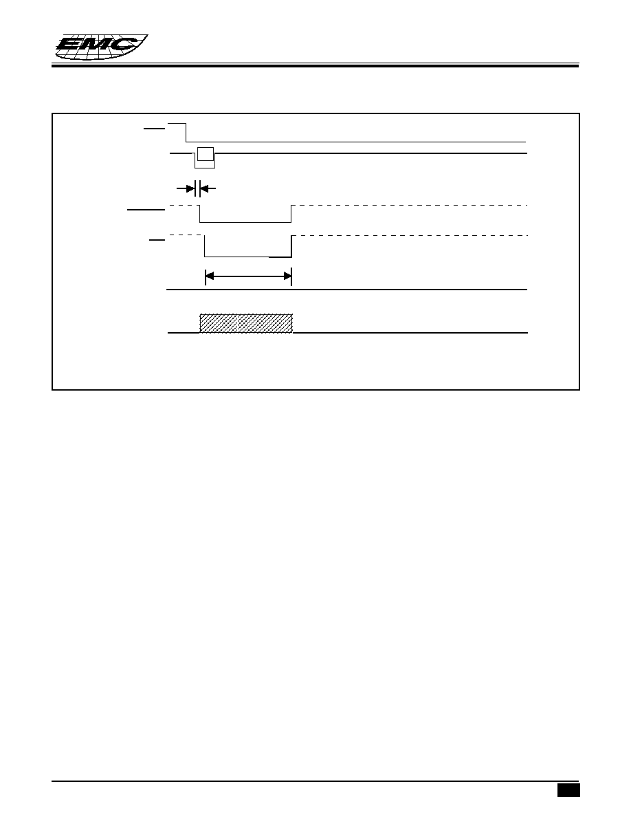
Figure 8: Flash key operation timimg
- - - - - - High impedance
HKS
KEY IN
TONE
OSCO
XMUTE
PO
t
DB
F
F
T

* This specification are subject to be changed without notice.
EM91710A/B
TONE/PULSE SWITCHABLE DIALER
14
9.30.1997
APPLICATION CIRCUIT
C1
C2
C3
C4
R1
R2
R3
R4
OSCI
OSCO
V
SS
PO
V
DD
HKS
TONE
7
12
2 WIRE TO 4 WIRE
SPEECH NETWORK
1µ
100K
TO HANDSEET
220K
100µ/16V
C945
9
470K
2K7
Z.D.
5V1
IN4148
IN4148
100µ
16V
.1µ
11
IN4148
330K
100K
MPSA42
2K2
MPSA92
100K
OFF
240K
HOOK SW
ON
22M
ZNR
120V
IN4004*4
Tip
Ring
1
4
7
*
2
5
8
0
3
6
9
#
P
T
F
P
R/P
820k*6
3.579545MHz
568
10
4
1
2
3
14
15
16
13
XMUTE
EM91710A
EM91710A Application Example
TONE
20PPS
10PPS
V
DD
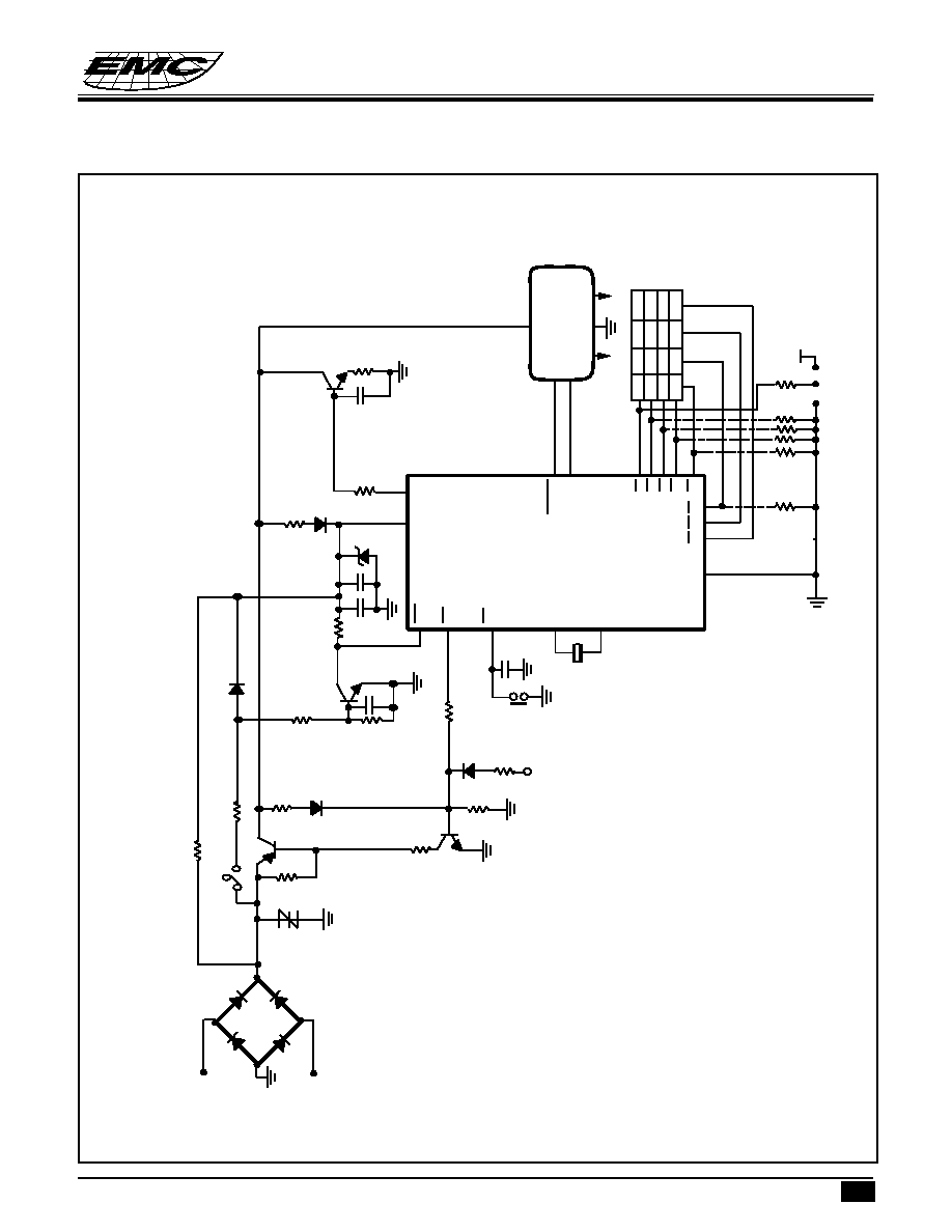
15
EM91710A/B
TONE/PULES SWITCHABLE DIALER
* This specification are subject to be changed without notice.
9.30.1997
APPLICATION CIRCUIT
.02µ
200
C945
IN4148
EM91710B Application Example
2K2
IN4148
C945
3K3
ZNR
120V
HOOK ON
MPSA92
100K
22M
Ring
Tip
IN4004*4
0.1µF
47K
V
DD
TONE
XMUTE
HKS
13
2 TO 4 WIRE
SPEECH NETWORK &
AUDIO AMPLIFIER
EM91710B
1
4
7
*
2
5
8
0
3
6
9
#
P
T
F
P
RD
OSCO
OSCI
9
C4 C3 C2
PO
R1
R2
R3
R4
HFI
17
18
15
21
4
3
16
V
SS
HFO
8
TO HANDSET
100K
12
11
14
+
1µ
470K
100µ
16V
+
.1µ
5V1
C945
200K
5
7
10
.1µ
240K
820K*6
330K
100K
47K
HFO
6
HF
KEY
3.579545 MHz
C1
V
DD
TONE
20PPS
10PPS
2K7
* This specification are subject to be changed without notice.
EM91710A/B
TONE/PULSE SWITCHABLE DIALER
16
9.30.1997
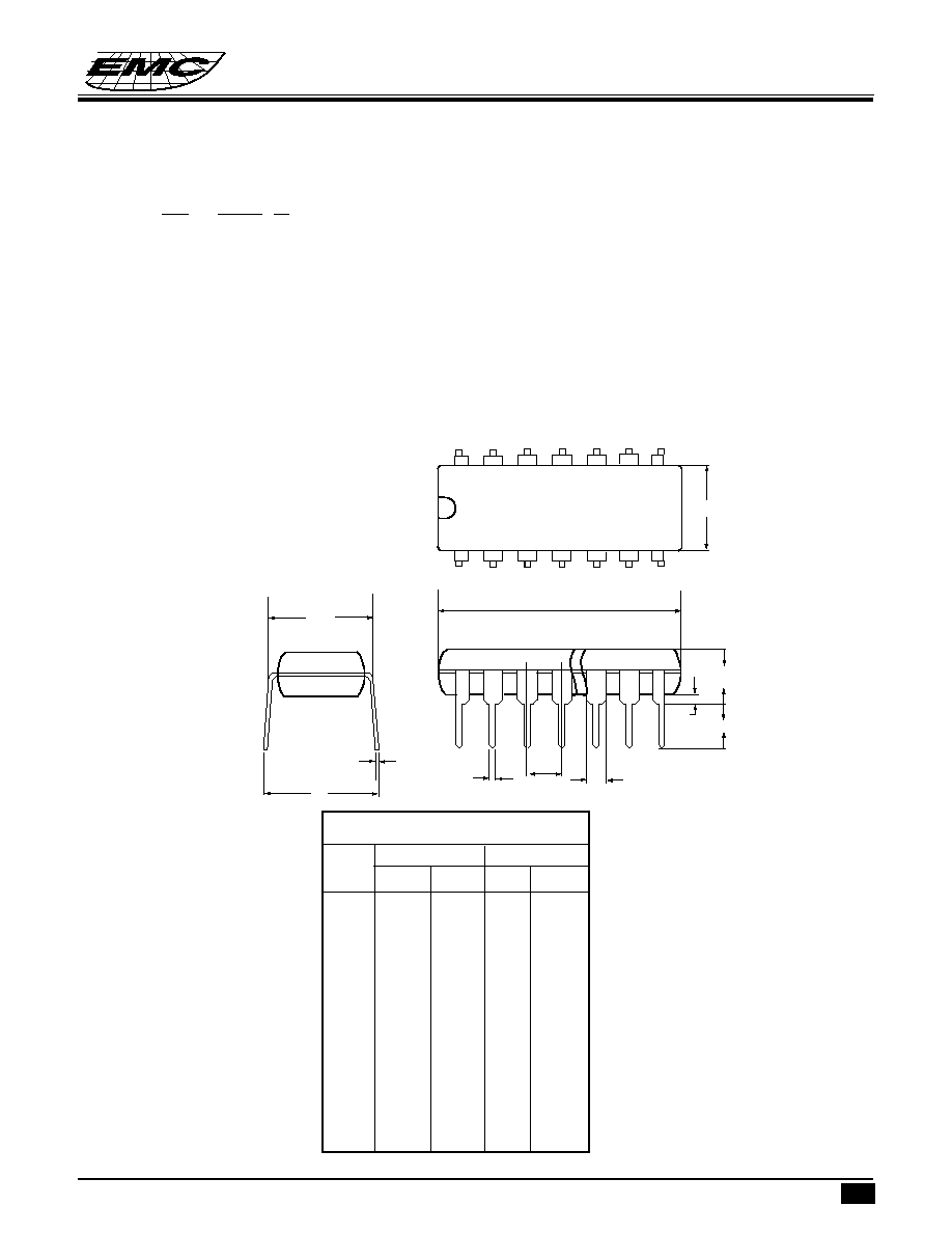
16 PDIP
MILIMETERS
INCHES
DIM
MIN.
MAX. MIN. MAX.
A
-
5.334
-
.210
A1
0.381
-
.015
-
B
0.356
0.558
.014
.022
B1
1.150
1.778
.045
.070
C
0.204
0.381
.008
.015
D
19.05
20.07
.750
.790
E
7.620
8.255
.300
.325
E1
6.096
7.112
.240
.280
e
2.286
2.794
.090
.110
eB
-
10.92
-
.430
L
2.921
4.064
.115
.160
Example :
EM
91710 P
(1)
(2)
(3)
(1) ELAN MICRO. pefix
(2) Type number
(3) Package code:
P
PDIP
K
Skinny
R
SDIP
PACKAGE INFORMATION
16 Lead Plastic Package
B
C
eB
D
E1
B1
A1
e
L
A
E
1

17
EM91710A/B
TONE/PULES SWITCHABLE DIALER
* This specification are subject to be changed without notice.
9.30.1997
18 PDIP
MILIMETERS
INCHES
DIM
MIN.
MAX. MIN. MAX.
A
-
5.334
-
.210
A1
0.381
-
.015
-
B
0.356
0.558
.014
.022
B1
1.150
1.778
.045
.070
C
0.204
0.381
.008
.015
D
22.35
23.37
.880
.920
E
7.620
8.255
.300
.325
E1
6.096
7.112
.240
.280
e
2.286
2.794
.090
.110
eB
-
10.92
-
.430
L
2.921
4.064
.115
.160
20 PDIP
MILIMETERS
INCHES
DIM
MIN.
MAX.
MIN.
MAX.
A
-
5.334
-
.210
A1
0.381
-
.015
-
B
0.356
0.558
.014
.022
B1
1.150
1.778
.045
.070
C
0.204
0.381
.008
.015
D
25.40
26.67
1.000
1.050
E
7.620
8.255
.300
.325
E1
6.096
7.112
.240
.280
e
2.286
2.794
.090
.110
eB
-
10.92
-
.430
L
2.921
4.064
.115
.160
28 PDIP
MILIMETERS
INCHES
DIM
MIN.
MAX. MIN.
MAX.
A
-
6.350
-
.250
A1
0.381
-
.015
-
B
0.356
0.558
.014
.022
B1
1.016
1.778
.040
.070
C
0.204
0.381
.008
.015
D
35.56
37.85 1.400
1.490
E
15.24
15.88
.600
.625
E1
13.21
14.73
.520
.580
e
2.286
2.794
.090
.110
eB
-
17.78
-
.700
L
2.921
5.080
.115
.200
B
C
eB
D
E1
B1
A1
e
L
A
E
1
18/20/28 Lead Plastic Package

* This specification are subject to be changed without notice.
EM91710A/B
TONE/PULSE SWITCHABLE DIALER
18
9.30.1997
22/24 Lead Plastic Package-Skinny
22 PDIP (skinny)
MILIMETERS
INCHES
DIM
MIN.
MAX.
MIN.
MAX.
A
-
4.752
-
.180
A1
0.381
-
.015
-
B
0.356
0.558
.014
.022
B1
1.27
1.778
.050
.070
C
0.204
3.556
.008
.014
D
25.90
26.67
1.02
1.05
E
7.620
8.255
.300
.325
E1
6.223
6.604
.245
.260
e
2.286
2.794
.090
.110
eB
8.382
10.16
.330
.400
L
2.921
4.064
.115
.160
24 PDIP (skinny)
MILIMETERS
INCHES
DIM
MIN.
MAX.
MIN.
MAX.
A
-
4.572
-
.180
A1
0.381
-
.015
-
B
0.356
0.558
.014
.022
B1
1.27
1.778
.050
.070
C
0.204
0.381
.008
.015
D
31.24
32.26
1.23
1.270
E
7.620
8.255
.300
.325
E1
6.223
6.731
.245
.265
e
2.286
2.794
.090
.110
eB
8.636
9.652
.340
.380
L
2.921
4.064
.115
.160
B
C
eB
D
E1
B1
A1
e
L
A
E
1
19
EM91710A/B
TONE/PULES SWITCHABLE DIALER
* This specification are subject to be changed without notice.
9.30.1997
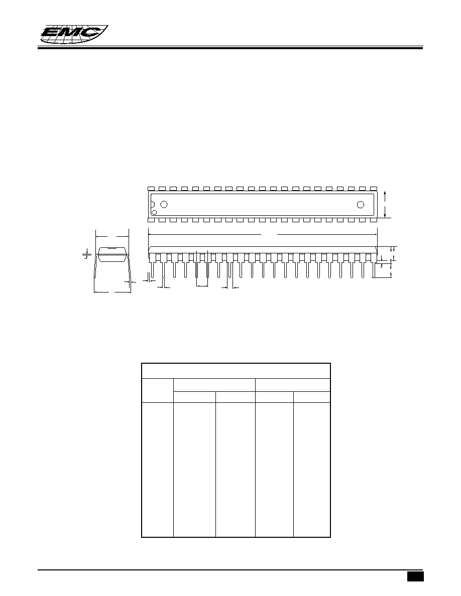
42 SDIP Package
B
D1
C
eB
D
B1
A1
e
L
A A2
E
E1
42 SDIP
MILIMETERS
INCHES
DIM
MIN.
MAX.
MIN.
MAX.
A
-
5.08
-
0.200
A1
0.381
-
0.015
-
A2
3.937
4.191
0.155
0.165
B
0.356
0.559
0.014
0.022
B1
0.914
1.116
0.036
0.044
C
0.204
0.304
0.008
0.012
D
36.70
37.34
1.445
1.470
E1
13.84
14.10
0.545
0.555
e
1.727
1.829
0.068
0.072
eB
15.24
17.78
0.600
0.70
D1
0
0.127
0
0.005
L
2.921
3.429
0.115
0.135