EM4069
EM4169
Copyright
2003, EM Microelectronic-Marin SA
1
www.emmicroelectronic.com
128 bit Read/Write Contactless Identification Device
with OTP function
Description
EM4069 (previously named P4069) is a CMOS integrated
circuit intended for use in electronic Read/Write RF
transponders, with an optional lock function to disable
EEPROM write operations.
The IC is powered by picking the energy from a
continuous 125 kHz magnetic field via an external coil,
which together with the integrated capacitor form a
resonant circuit. The IC read out data's from its internal
EEPROM or ROM and sends it out by switching on and
off a resistive load in parallel to the coil. Commands and
EEPROM data updates can be executed by AM
modulation of the 125 kHz magnetic field.
At power≠up the EM4069 goes in default mode in which it
constantly (without any pause) transmits 128 bits from the
EEPROM. Upon transmission of a specific command, the
64 bits unique laser code is output. Additional commands
for writing and lock data in EEPROM are available.
The EM4169 (previously named P4169) is the same
device but with large bumps (mega pads) as indicated on
page 13 of this data sheet. All specified parameters and
descriptions are applicable for the EM4169 device.
Features
128 bit EEPROM organized in 8 words of 16 bits
64 bit fixed code memory array laser programmed
OTP feature convert EEPROM words in read only
Power on Reset sequence
Power-check for EEPROM write operation
Data transmission performed by Amplitude
Modulation (IC to reader and reader to IC)
Data encoding : Manchester or BI-Phase (FDX-B)
Transmission reader to chip: typically 65% AM
modulation
Data rate : 64 or 32 RF field periods per bit
(2 kBaud or 4 kBaud at 125 kHz)
78 pF resonant capacitor integrated on chip
100 to 150 kHz frequency range
On-chip rectifier and voltage limiter
No external supply buffer capacitor needed
-40 to +85
∞C temperature range
Very low Power consumption
Applications
Access Control
Animal Identification
Material Logistics
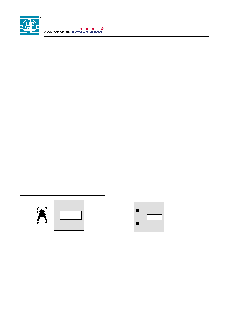
Typical Operating Configuration
VSS
L
C1
Typical value for inductance L is 20.7mH at
f
O
= 125
KHz
EM4069
Fig. 1
Pin Assignment
EM4069
C1
VSS
Fig. 2
EM MICROELECTRONIC
- MARIN SA

EM4069
EM4169
Copyright
2003, EM Microelectronic-Marin SA
2
www.emmicroelectronic.com
Absolute Maximum Ratings
V
SS
= 0V
Parameter
Symbol
Conditions
Power supply
V
DD
-0.3 to +5.5V
Input Voltage (pads TST,
TCP, TIO)
V
PIN
- 0.3 to
VDD+0.3V
Input current on COIL1
I
COIL1
-30 to
+30mA
Input voltage on COIL1
V
COIL1
-10 to +10V
Storage temperature
T
STORE
-55 to
+125∞C
Electrostatic discharge to
MIL-STD-883C method 3015
V
ESD
1000V
Stresses above these listed maximum ratings may cause
permanent damage to the device. Exposure beyond
specified electrical characteristics may affect device
reliability or cause malfunction.
Electrical parameters and functionality are not
guaranteed when the circuit is exposed to light.
Handling Procedures
This device has built-in protection against high static
voltages or electric fields. However due to the unique
properties of this device, anti-static precautions should
be taken as for any other CMOS component. Unless
otherwise specified, proper operation can only occur
when all terminal voltages are kept within the supply
voltage range.
Operating Conditions V
SS
= 0V
Parameter
Symbol Min.
Typ. Max. Units
Operating temperature
AC voltage on coil 1
Maximum coil current
Frequency on coil 1
T
OP
V
COIL1
I
COIL1
F
COIL1
-40
-10
100
+25
*
125
+85
10
150
∞C
Vpp
mA
kHz
*) Maximum voltage is defined by forcing 10mA on
Coil1 ≠ Vss
Electrical Characteristics
Unless otherwise specified: V
DD
= 1.0V to 5.5V, T
A
=-40 to +125∞C.
Parameter
Symbol
Condition
Min.
Typ.
Max.
Units
Regulated Supply Voltage
V
DD
I
COIL1
= 10mA
3.0
3.5
4.0
V
Reg. Voltage reading EEPROM (note 3)
V
RD
2.0
V
Supply current in read mode
I
RD
3.8
5,5
µA
Reg. Voltage writing EEPROM
V
WR
2.5
V
Supply current write mode
I
WR
V
DD
= 3.5 V
50
100
µA
Power Check Voltage
V
PC
2.4
2.8
3.15
V
Modulator ON voltage drop
V
on1
I
COIL1
= ±100
µA
1.2
1.45
1.75
V
Modulator ON voltage drop
V
on2
I
COIL1
= ±1 mA
3
3.6
4.5
V
POR level
V
POR
Rising edge
1.5
1.85
2.20
V
Clock extractor
V
COIL1
0.5
V
PP
Peak detector threshold.
V
pd
V
DD
= 3.3 V
3.2
4
4.6
V
PP
Peak detector hysteresis
V
pdh
V
DD
= 3.3 V
20
100
200
mV
Resonance capacitor (note 1)
C
R
32 kHz, 0.3Vpp
78
pF
EEPROM data retention (note 2)
T
RET
T
OP
= 55∞C
10
years
EEPROM write cycles
N
CY
V
DD
= 3.6 V
100000
cycles
Note 1:
Value of the resonance capacitor may vary in limits of
± 12%
Statistics show a variation of capacitance within one lot of
± 5%.
These figures are given as information only.
Note 2:
Based on 1000 hours at 150∞C.
Note 3:
V
RD
must be higher than V
POR
Level.

EM4069
EM4169
Copyright
2003, EM Microelectronic-Marin SA
3
www.emmicroelectronic.com
Timing Characteristics
V
DD
= 3.0 V, V
SS
= 0 V, f
COIL1
= 125 kHz square wave, V
COIL1
= 5V, T
OP
= 25∞C, unless otherwise specified
Parameter
Symbol
Condition
Min.
Typ.
Max.
Unit
Option : 64 RF periods per bit
Read bit period
t
RDB
64
RF periods
EEPROM write time
t
Wee
20
ms
Synchronization pattern phase 1
t
S1
4.1
5.0
ms
Synchronization pattern phase 2
t
S2
1.5
2.0
ms
Synchronization pattern phase 3
t
S3
1.5
4.0
ms
Option : 32 RF periods per bit
Read bit period
t
RDB
32
RF periods
EEPROM write time
t
Wee
20
ms
Synchronization pattern phase 1
t
S1
2.1
2.5
ms
Synchronization pattern phase 2
t
S2
0.8
1.0
ms
Synchronization pattern phase 3
t
S3
0.8
2.0
ms
RF periods represent periods of the carrier frequency emitted by the transceiver unit.
See figure 12 for Synchronization pattern phases.
Due to amplitude modulation of the coil-signal, the clock-extractor may miss clocks or add spurious clocks close to
the edges of the RF-envelope. This desynchronization will not be larger than
±
±
±
± 3 clocks per bit and must be taken into
account when developing reader software.
Block Diagram
Modulator
Control
Logic
EEPROM
Clock
Extractor
Sequencer
Data
Extractor
C
R
C
buf
VDD
VSS
Power
Supply
Reset
Power on
Reset
COIL1
VSS
ROM
Fig. 3

EM4069
EM4169
Copyright
2003, EM Microelectronic-Marin SA
4
www.emmicroelectronic.com
Functional Description
The IC builds its power supply through an integrated
rectifier. When it is placed in a magnetic field the DC
internal voltage starts to increase.
As long the power supply is lower than the power on reset
(POR) threshold, the circuit is in reset mode to prevent
unreliable operation. In this mode the modulator switch is
off.
After the supply voltage cross the POR threshold, the
circuit goes in read mode and transmits periodically the
128 data bits from EEPROM.
The power on reset is designed with a typically 250mV
hysteresis. The specified value in the DC electrical
characteristic table indicates the high level-switching
threshold. Ones the supply voltage had reached this level,
the device work in read mode and reenter in reset mode if
the supply voltage decrease under the lower threshold
(~V
POR
≠ 250mV).
In read mode the IC transmits periodically either the 128
data bits from EEPROM or 64 data bits from ROM if
command 2 has been sent. The bits are Manchester or BI-
phase coded and issued by switching the modulator load in
parallel to the coil ON and OFF. The read out process is
repeated continuously without any pause as long as power
level is greater than the POR threshold low.
While the IC is operating in read mode it checks the coil
signal once every bit period. If it detects a certain reader
induced amplitude modulation of magnetic field it stops
modulating and waits for a command word. In the case the
EEPROM write command is detected the contents of
selected EEPROM word is modified. Read ROM command
will change the output sequence to the data provided by
the laser ROM continuously.
The Reset command returns to the initial mode as after a
Power on Reset.
Block description
Power On Reset (POR)
When the EM4069 with its attached coil enters an
electromagnetic field, the built in AC/DC converter will
supply the chip. The DC voltage is monitored and a Reset
signal is generated to initialise the logic. The Power On
Reset is also provided in order to make sure that the chip
will start issuing correct data.
Hysteresis is provided to avoid improper operation at the
limit level.
VPOR
t
Reset
VDD
t
Hysteresis
P4069 Active
Fig. 4
Clock Extractor
The Clock extractor will generate a system clock with a
frequency corresponding to the frequency of the RF field.
The system clock is used by a sequencer to generate all
internal timings.
Data Extractor
The transceiver generated field will be amplitude
modulated to transmit data to the EM4069. The Data
extractor demodulates the incoming signal to generate
logic levels, and decodes the incoming data.
Modulator
The Data Modulator is driven by the serial data output from
the transceiver. The modulator will draw a large current
from both coil terminals, thus amplitude modulating the RF
field according to the selected memory data.
AC/DC Converter and Voltage Limiter
The AC/DC converter is fully integrated on chip and will
extract the power from the incident RF field. The internal
DC voltage will be clamped to avoid high voltage in strong
RF fields.
Lock All / Lock Memory Area
The EM4069 can be converted to a Read Only chip or be
configured to Read/Write and Read Only Areas by
programming the protection word. This configuration can
be locked by write inhibiting the Write Protection Word.
Great care should be taken in doing this operation as there
is no further possibility to change the Write Protection
Word. The Control Word can also be protected in the
same way thus freezing the writing operation.
EM4069 Active

EM4069
EM4169
Copyright
2003, EM Microelectronic-Marin SA
5
www.emmicroelectronic.com
EM4069 Modes of operation
Sync-Pattern
INIT
EEPROM Read Mode
Command State
RF-field detected
IDLE
Reset
Command
Command finished
Fig. 5
Read Mode
The EM4069 holds 128 bits of user EEPROM. These 128
bits are cyclically read out by default. Using the write
command, the EEPROM words can be modified. The
EEPROM contains an additional configuration word used
to protect writing in the
EEPROM
The EM4069 additionally holds a unique 64 bit read only
identification code, which can be accessed by using the
Read ROM command.
Manchester encoding
One bit period lasts 64 (or 32) field frequency periods
(512 (or 256)
µs at 125 kHz). The Manchester coding
shows a transition from ON to OFF or from OFF to ON in
the middle of bit period. At the transition from logic bit "1"
to logic bit "0" or logic bit "0" to logic bit "1" the phase
change. Value "high" of data stream presented below
represents modulator switch OFF, "low" represents
switch ON (see figure 6a).
Bi-phase encoding
One bit period lasts 64 (or 32) field frequency periods
(512 (or 256)
µs at 125 kHz). The BI-phase coding shows
a transition from ON to OFF or from OFF to ON in the
middle of a bit period when the data bit is a logical "0". A
logical bit set to "1" will keep its ON or OFF state for the
whole bit period. There is always a transition from ON to
OFF or from OFF to ON at the beginning of a bit period.
The picture below shows part of a data stream. Value
"high" of data stream represents modulator load OFF,
"low" represents modulator load ON (see figure 6b).
Manchester encoding
X 1
1
1
1
1
1
1
1
1
0
1
0
1
0
0
0
1
1
0
Binary data
Memory output
Modulator control
Modulation control "low" means high current
Fig. 6a
Bi-phase encoding
0
1
1
0
1
0
0
1
Modulation control "low" means high current
Binary data
Memory output
Modulator control
Fig. 6b