 | –≠–ª–µ–∫—Ç—Ä–æ–Ω–Ω—ã–π –∫–æ–º–ø–æ–Ω–µ–Ω—Ç: EM7604 | –°–∫–∞—á–∞—Ç—å:  PDF PDF  ZIP ZIP |
Document Outline
- ˛ˇ
- ˛ˇ
- ˛ˇ
- ˛ˇ
- ˛ˇ
- ˛ˇ
- ˛ˇ
- ˛ˇ
- ˛ˇ
- ˛ˇ
- ˛ˇ
- ˛ˇ
- ˛ˇ
- ˛ˇ
- ˛ˇ
- ˛ˇ
- ˛ˇ
- ˛ˇ
- ˛ˇ
- ˛ˇ
- ˛ˇ
- ˛ˇ
R
EM7604
Copyright
© 2006, EM Microelectronic-Marin SA
03/06 ≠ rev.A
1
www.emmicroelectronic.com
Low Power Crystal Oscillator 32.768 kHz
Description
The EM7604 is an advanced low power CMOS circuit
intended to be used together with a 32.768 kHz tuning fork
crystal as a low frequency clock oscillator.
Except the crystal, no other external components are
required.
In order to achieve a high frequency accuracy, the matched
crystals should have a ± 20ppm tolerance or tighter.
Very low power consumption, as low as 250nA, is
guaranteed over a very wide supply voltage and
temperature ranges.
Offered in a small SOT23-6 package, the EM7604 is a
completely lead free product.
Applications
General purpose clock generator for digital systems
Clock drivers for Real Time Clocks
Timekeeping in network servers and computers
Electricity, gas and water metering
Portable field communication
Mobile phone
Solution for problems with embedded quartz oscillators
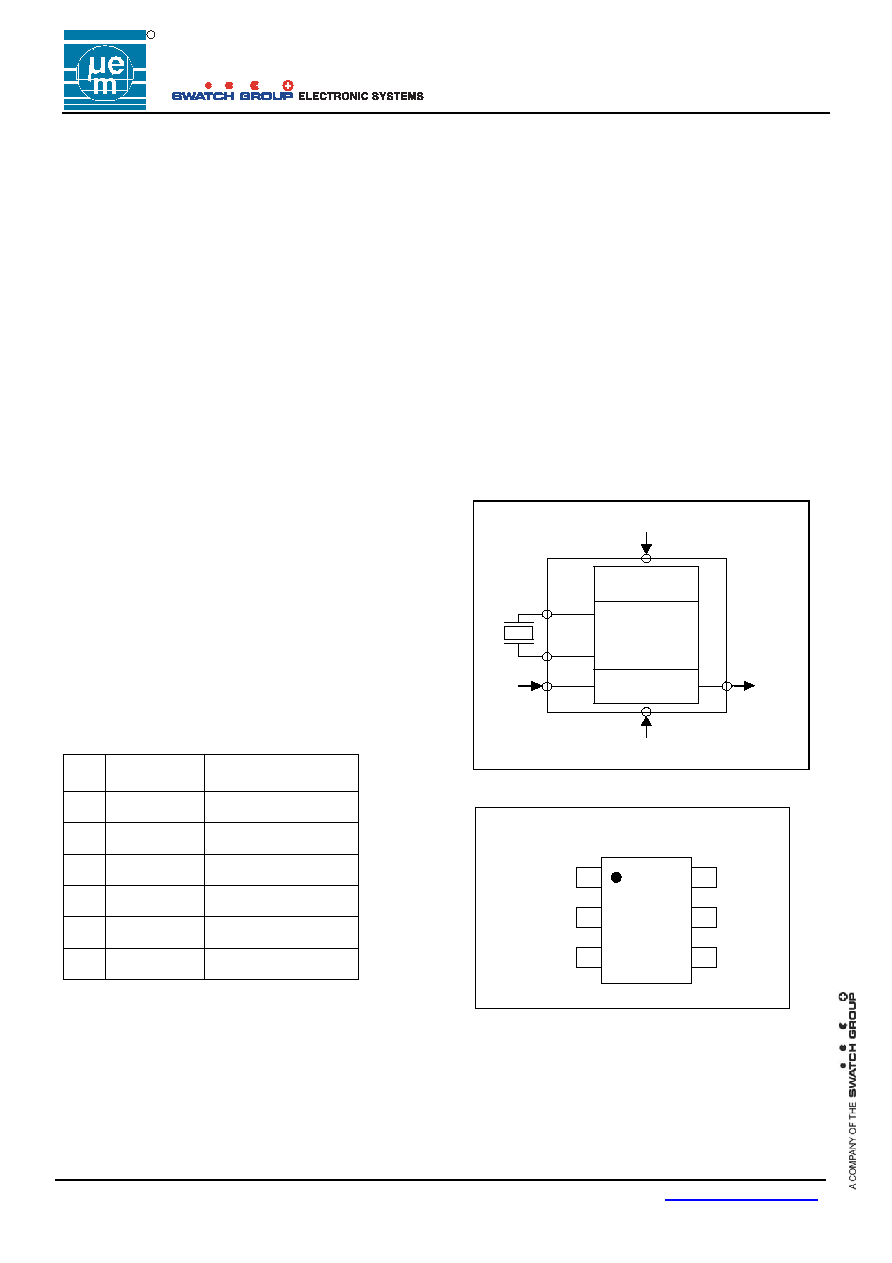
Pin Assignment
Features
Very low power consumption: typ. 250nA
On chip integrated oscillation capacitor: C
L
=8pF
Matched low cost SMD quartz available from Micro Crystal
Compatibility with crystals having high series resistance
Very tight frequency tolerance
Excellent oscillator stability: 0.2ppm/V
Wide supply voltage range: 1.2V to 5.5V
Operating temperature range: -40∞C to +125∞C
Small SOT23-6 package
100% lead free, RoHS ≠ compliant
Block Diagram
OSCILLATOR
OUT
OE
VDD
VSS
OUTPUT
CONTROL
REGULATION
1
VSS
EM7604
2
3
OSCOUT
OSCIN
6
5
4
OE
VDD
OUT
SOT23
Pin Connection Assignment
1
OSCOUT
Oscillator Output
2
VSS
Negative Supply
Voltage
3
OSCIN
Oscillator Input
4
OE
Output Enable
5
VDD
Positive Supply
Voltage
6
OUT
Frequency Output
EM MICROELECTRONIC -
MARIN SA
R
EM7604
Copyright
© 2006, EM Microelectronic-Marin SA
03/06 ≠ rev.A
2
www.emmicroelectronic.com
Absolute Maximum Ratings
Parameter Symbol
Conditions
Voltage at V
DD
to V
SS
V
DD
-0.3V to +6V
Minimun voltage
V
MIN
V
SS
≠ 0.3V
Maximun voltage
V
MAX
V
DD
+ 0.3V
Storage Temperature Range
T
STG
-55∞C to +150∞C
Maximum soldering
T
Smax
260∞C x 20s
Stresses above these listed maximum ratings may cause
permanent damages to the device. Exposure beyond
specified operating conditions may affect device reliability
or cause malfunction.
Handling Procedures
This device has built-in protection against high static
voltages or electric fields; however, anti-static precautions
must be taken as for any other CMOS component. Unless
otherwise specified, proper operation can only occur when
all terminal voltages are kept within the voltage range.
Unused inputs must always be tied to a defined logic
voltage level.
Operating Conditions
Parameter Symbol
Min
Max
Unit
Supply voltage
V
DD
1.2 5.5
V
Operating Temperature
T
A
-40
+125
∞C
Electrical Characteristics
Unless otherwise specified: V
DD
= 3.0V, V
SS
= 0V, T
A
=25∞C and R
S
= 60k
Parameter Symbol
Conditions
Min
Typ
Max
Unit
Supply voltage range
V
DD
1.2
3.0
5.5
V
Current consumption
I
DD1
V
DD
= 5.0V, OE at V
SS
300
550
nA
(Note1)
V
DD
= 3.0V, OE at V
SS
250
500
nA
V
DD
= 2.0V, OE at V
SS
250
500
nA
V
DD
= 5.0V, OE at V
SS
Top=-40 to +85∞C
750
1000
nA
V
DD
= 3.0V, OE at V
SS
Top=-40 to +85∞C
650
900
nA
V
DD
= 2.0V, OE at V
SS
Top=-40 to +85∞C
650
900
nA
Oscillator
Input Capacitance
C
IN
16
pF
Output Capacitance
C
OUT
16
pF
Start Up Voltage
V
STARTUP
t
START
< 3s
1.2
Start Up Time
t
STARTUP
0.4
0.8
s
Frequency Stability against
Supply Voltage Variations
f/f *V 1.5 V
DD
5.5V
0.2
2
ppm/V
Input
Input Voltage
V
IL
V
SS
0.2 x V
DD
V
V
IH
0.8 x V
DD
V
DD
V
Output
Duty Cycle
40
50
60
%
Output Voltage
V
OH
I
OH
= -1.0 mA, V
DD
= 5.0V
V
DD
-0.4 V
DD
-0.1 V
V
OL
I
OL
= 1.0 mA, V
DD
= 5.0V
0.14
0.4
V
Output Rise and Fall Time
t
RF
C
L
= 15pF
10% - 90%
70
100
ns
Note1: The current consumption when the output clock is enabled (OE pin at V
DD
) is a function of the load capacitance on the
OUT pin, the output frequency f
OUT
= 32768Hz
and the supply voltage V
DD
.
The additional consumption for a given load can be calculated from: I
DD =
C
LOAD
x V
DD
x f
O
R
EM7604
Copyright
© 2006, EM Microelectronic-Marin SA
03/06 ≠ rev.A
3
www.emmicroelectronic.com
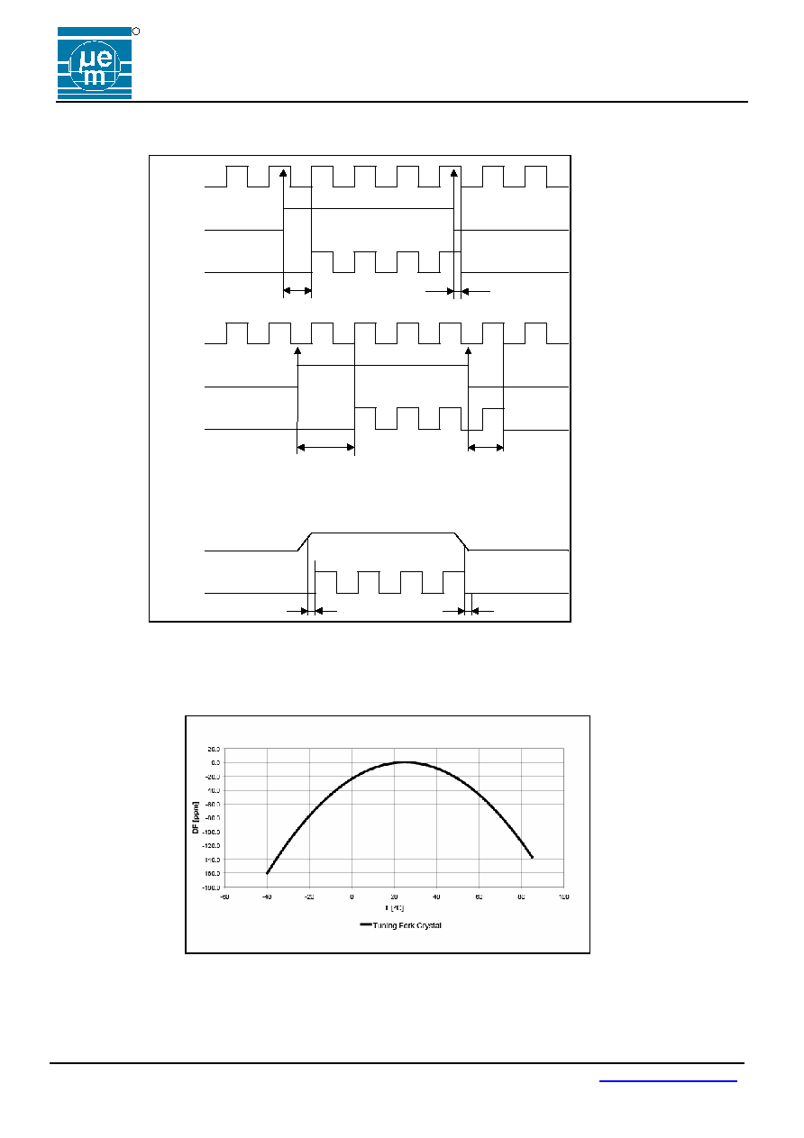
Timing Waveforms
32768Hz
OE
OUT
32768Hz
OE
OUT
OE
OUT
V
IH
V
IL
t
CKH
t
CKL
t
CKH
t
CKH
t
CKL
t
CKL
Frequency Temperature Characteristics with Standard 32.768 kHz Crystal
R
EM7604
Copyright
© 2006, EM Microelectronic-Marin SA
03/06 ≠ rev.A
4
www.emmicroelectronic.com
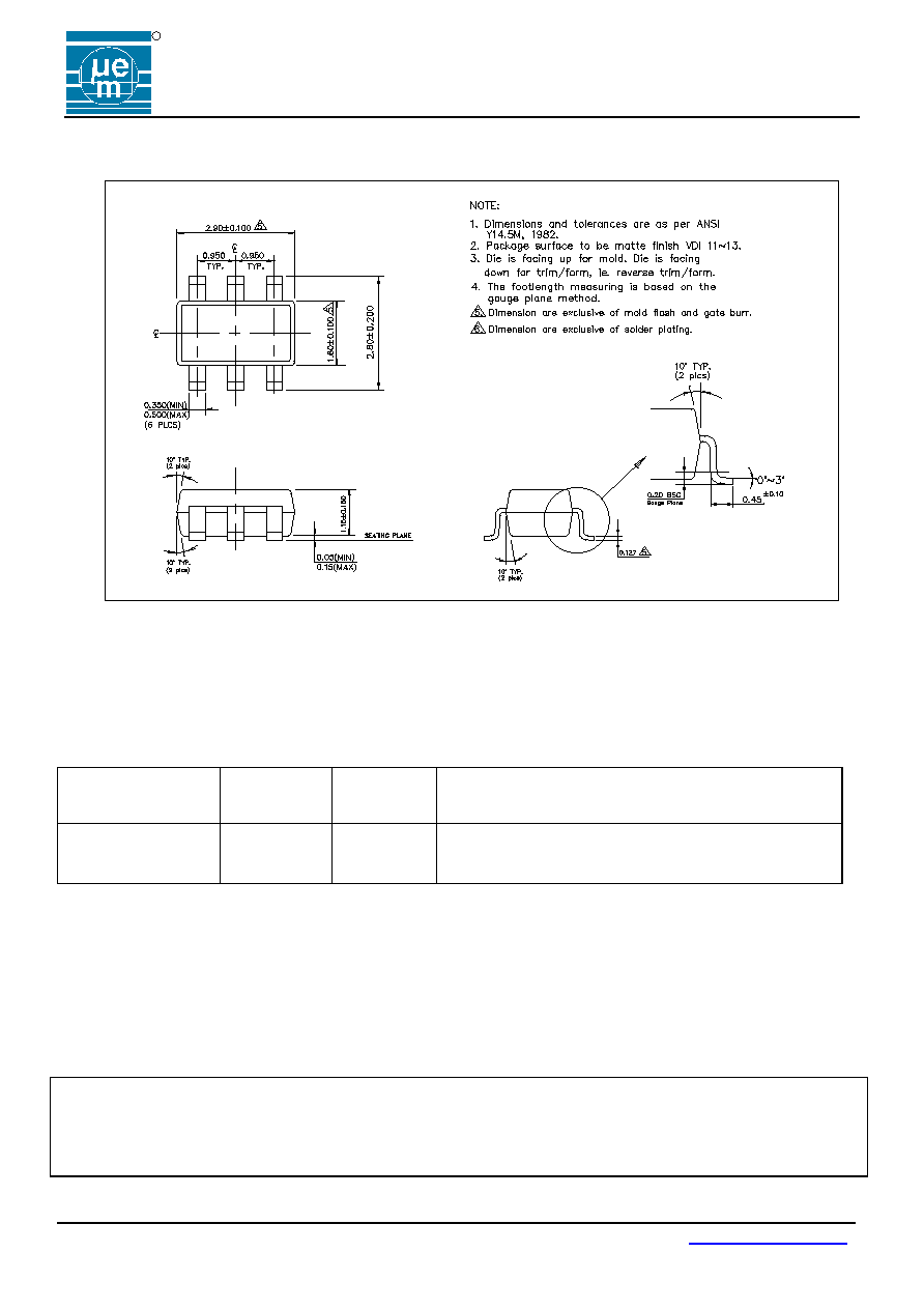
Package Information:
Ordering Information
Part Number
Package Type
Top Marking
Delivery Form
EM7604V1SP6B+
SOT23
OVXY
Tape & Reel
Contact EM Microelectronic for availability in chip form or in other packages.
XY characters of the Top Marking are used for the lot traceability.
EM Microelectronic-Marin SA (EM) makes no warranty for the use of its products, other than those expressly contained in the
Company's standard warranty which is detailed in EM's General Terms of Sale located on the Company's web site. EM assumes
no responsibility for any errors which may appear in this document, reserves the right to change devices or specifications
detailed herein at any time without notice, and does not make any commitment to update the information contained herein. No
licenses to patents or other intellectual property of EM are granted in connection with the sale of EM products, expressly or by
implications. EM's products are not authorized for use as components in life support devices or systems.