 | –≠–ª–µ–∫—Ç—Ä–æ–Ω–Ω—ã–π –∫–æ–º–ø–æ–Ω–µ–Ω—Ç: H1137V02 | –°–∫–∞—á–∞—Ç—å:  PDF PDF  ZIP ZIP |

R
H1137
Copyright
© 2004, EM Microelectronic-Marin SA
1
www.emmicroelectronic.com
CMOS circuit for Analog Quartz Watches
Description
The H1137 is a low power 32kHz analog watch chip de-
signed to drive a stepping motor. Motor pulse width is
programmable from 0.9765 to 14.65 milliseconds in steps
of 0.9765 milliseconds. Motor pulse period is program-
mable from 2 x 1 to 2 x 60 seconds in steps of 1 second.
Motor pulse period is also programmable from 2 x 0.25 to
2 x 15.75 seconds in steps of 0.25 seconds. Input and
output capacitors are integrated on the chip. Their values
are metal mask selectable. The selection of width, period
and capacitance are metal options and do not require
additional bonds.
Application
Analog watches
Features
32Hz quartz oscillator
Operating voltage range ≠ 1.2V to ≠1.8V
High oscillator stability
Integrated capacitors, mask selectable
Mask options for pad designation, motor period and
motor pulse width
Shorted motor coil between motor pulses
Fast motor test function
ESD protected terminals
512Hz output on TEST pad for quartz frequency
measurement
Fully debounced TEST input and RESET input
Functional Diagram
Operating range of Trimmer Capacitance:
3pF
C
TR
30 pF
RL
(Stepping Motor)
CROWN
C
TR
V
N
V
P
V
P
V
P
RESET
MOT
1
MOT
2
OSC
IN
OSC
OUT
H1137
V
P
V
N
Fig. 1
Pin Assignment
H1137
8
7
6
5
1
2
3
4
10
Pad
Function
Pad
location
V
N
Negative
supply
voltage 1
V
P
Positive supply voltage
5
OSC
IN
Oscillator
input
3
OSC
OUT
Oscillator
output
4
MOT
1
Motor drive output 1
7
MOT
2
Motor drive output 2
6
RESET Reset input
2 or 8
TEST
Test input/output
2 or 8 or 10
Fig. 2
EM MICROELECTRONIC -
MARIN SA

R
H1137
Copyright
© 2004, EM Microelectronic-Marin SA
2
www.emmicroelectronic.com
Absolute Maximum Ratings
Parameter
Symbol Min. Typ. Max. Units
Supply voltage
Voltage applied
to other terminals
Storage tem-
perature
V
N
T
STOR
-3.6
V
N
≠0.3
-55
+0.2
V
P
+0.3
+125
V
V
∞C
Stresses beyond these listed maximum ratings may
cause permanent damage to the device. Exposure to
conditions beyond specified operating conditions may
affect device reliability or cause malfunction.
Recommended Operating Conditions
Parameter Symbol
Value
Units
Ambient temperature
Quartz frequency
Quartz series resistance
Motor coil resistance
Positive supply
Negative supply
Supply source resistance
T
f
Q
R
Q
R
M
VP
V
N
R
I
25
32768
30
2.0
0
-1.55
10
∞C
Hz
k
k
V
V
Handling Procedures
This device contains circuitry to protect the terminals
against damage due to high static voltages or electrical
fields. However, it is advised that normal precautions be
taken to avoid application of any voltage higher than
maximum rated voltages to this circuit.
Operating Conditions
Parameter Symbol
Min.
Typ.
Max.
Units
Operating temperature
Quartz series resistance
Trimmer capacitance
T
OPR
C
TR
-10
3
30
+60
50
30
∞C
k
pF
Electrical and Switching Characteristics
at recommended operating conditions unless otherwise specified
Parameter Symbol
Test
Conditions
Min.
Typ.
Max.
Units
Supply voltage range
Mean dynamic current
V
N
I
DYN
Without motor and quartz,
32kHz inverted square wave forced
at OSC
IN
and OSC
OUT
, TEST open
-1.8 -1.55
90
-1.2
150
V
nA
Mean current consumption
I
N
With quartz, without motor,
TEST open, C
TR
= 12 pF
200
350 nA
Oscillator
Transconductance
Starting voltage
Starting time
gm
V
ST
T
ST
V
N
= 1.2V, V
PP
= 300mV
Within 10 seconds
Recommended operating conditions
2.5
0.75
2
µmho
V
s
Stability df / f*dV
N
Between ≠1.4V and ≠1.6V
1.5
ppm/V
Motors Drivers
Voltage across motor
Voltage across motor
Voltage across motor
Short circuit impedance
V
MOT
V
MOT
V
MOT
R
CC
V
N
= -1.55V, R
M
= 2k
V
N
= -1.25V, R
M
= 2k
R
I
= 300 , T
OPR
Between motor pulses
1.35
1.0
1.0
1.40
1.10
1.20
150
300
V
V
V
Test Input / Output
Amplitude
Mean current
V
TST
I
TST
ZI = 30pF // 1M
Pad connected to V
P
1.35
70
250
V
PP
nA
Reset Input
Debounce delay
Input current after debounce delay
*
T
S
I
S
Pad connected to V
P
7.81
7
23.43
50
ms
nA
* Is the average input current, modulated by a frequency of 64 Hz

R
H1137
Copyright
© 2004, EM Microelectronic-Marin SA
3
www.emmicroelectronic.com
Timing Waveforms
Fast motor test mode, TEST = V
P
V
P
V
N
V
P
V
N
MOT
1
MOT
2
2.93 ms
T 65.43 ms (16 Hz)
2.93 ms
T 34.18 ms (32 Hz)
TEST
V
P
V
N
TM/2
tm
62.50ms
or
31.25ms
TM/2
V
N
V
P
V
N
V
P
V
N
T
TST
= 1.953 ms
(512Hz output)
V
P
V
N
RESET
MOT
1
MOT
2
TEST
Motor drive output and reset
>23.43ms
debounce delay
<7.81ms
TM/2
TM
tm
V
N
V
P
V
N
V
P
V
N
T
TST
= 1.953 ms
(512Hz output)
V
P
V
N
RESET
MOT
1
MOT
2
TEST
Motor drive output in normal operation
Fig. 3
R
H1137
Copyright
© 2004, EM Microelectronic-Marin SA
4
www.emmicroelectronic.com
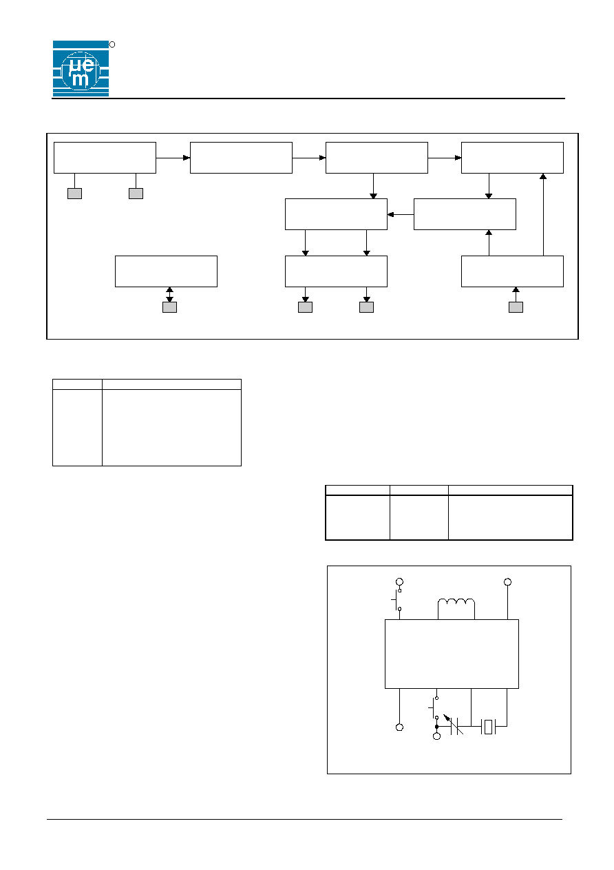
Block Diagram
O s c illa to r
In itia l D iv id e r
P u ls e W id th
D iv id e r
D iv id e r 1 H z
P u ls e R e p e titio n
D iv id e r
M o to r L o g ic
M a s te r R e s e t
M o to r D riv e r
T e s t L o g ic
O S C
IN
O S C
O U T
T E S T
M O T
1
M O T
2
R E S E T
Fig. 4
Pin Assignments
Name Function
V
N
V
P
OSC
IN
OSC
OUT
MOT
1
MOT
2
RESET
TEST
Negative supply voltage
Positive supply voltage
Oscillator input
Oscillator output
Motor drive output 1
Motor drive output 2
Reset input
Test input / output
Functional Description
Oscillator
The 32'768Hz clock frequency is generated by a crystal
oscillator. Input and output capacitors are integrated in
the chip. Their values are metal mask selectable.
Motor drive output
The H1137 contains two push-pull output buffers for driv-
ing bipolar stepping motors (see Fig. 3). Between two
pulses, the two p-channel devices are active for motor
damping.
Reset
Pulling the RESET input to V
P
resets the frequency di-
viders and disables the motor pulses. Motor pulses in
progress when the RESET function is applied, will be
completed. After releasing the RESET pad from V
P
, the
next motor pulse appears with a delay of one half motor
cycle on the drive output MOT
1
if the last motor pulse
appeared on MOT
2
or vice-versa (see Fig. 3). Due to the
debounce circuitry on the RESET input, V
P
must be ap-
plied for at least 23.4 ms to be accepted as RESET.
Test mode
The TEST pad fulfils two functions:
a) For normal operation, the TEST pad is left open. The
circuit outputs a square wave signal of 512Hz which
can be used for tuning the oscillator.
b) If the TEST pad is connected to V
P
, the period for
the motor pulses changes to either 2 x 31.25 ms or
2 x 62.5 ms (mask options), while the motor pulse
width remains unchanged (fast motor test).
Test
Test Pad
Function
Description
Connected to
V
P
Open
Fast motor
test
Normal
operation
Increase the frequency for the
motor pulses to 16Hz (32Hz)
Output of square wave signal
(512Hz)
Test configuration
Operating range of Trimmer Capacitance:
3pF
C
TR
30 pF
RL
Reset
C
TR
V
N
V
P
V
P
V
P
RES
E
T
MOT
1
MOT
2
OSC
IN
OSC
OU
T
H
113
7
V
P
V
N
TES
T
Test
Fig. 5

R
H1137
Copyright
© 2004, EM Microelectronic-Marin SA
5
www.emmicroelectronic.com
Metal Mask Option Possibilities
Motor pulse and capacitance
Sym-
bol
Description
Range
min.
Range
max.
Range
resolut.
TM
TM
tm
C
IN
C
OUT
Motor pulse period
Fast motor TEST
Motor pulse width
Oscillator input capacity
Oscillator output capac.
2x1.00s
2x31.25ms
0.9765ms
2pF
2.7pF
2x60.00s
2x62.50ms
14.65ms
C
IN
+ C
OUT
=35pF
1.00s
0.9765ms
1pF
1pF
Pad options
Sym-
bol
Description
Pad
Layout 1
Pad
Layout 2
Pad
Layout 3
TEST
RESET
Pad TEST
Pad RESET
Pad 10
Pad 8
Pad 2
not used
Pad 2
Pad 8
Pad 10
not used
Pad 8
Pad 2
Pad 10
not used
Possible versions
Option list (supply voltage ≠1.55V)
Options
Motor Output
Integrated
capacitor
Designation pad
Version
Period
s
Pulse
Width
ms
Fast
Mode
ms
OSC
IN
pF
OSC
OUT
pF
Pad 1
Pad 2 Pad 3
Pad 4
Pad 5
Pad 6
Pad 7
Pad 8 Pad 10
Com-
patible
EURO-
SIL
E1208
H1137V01
H1137V02
H1137V03
H1137V04
H1137V05
2x12
2x1
2x10
2x12
2x1
6.8
3.9
7.8
5.9
6.8
2x62.5
2x62.5
2x62.5
2x62.5
2x62.5
2
2
2
2
2
18
14
22
14
14
V
N
V
n
V
N
V
N
V
N
-
TEST
RESET
TEST
TEST
OSC
IN
OSC
IN
OSC
IN
OSC
IN
OSC
IN
OSC
OUT
OSC
OUT
OSC
OUT
OSC
OUT
OSC
OUT
V
P
V
P
V
P
V
P
V
P
MOT
2
MOT
2
MOT
2
MOT
2
MOT
2
MOT
1
MOT
1
MOT
1
MOT
1
MOT
1
RESET
RESET
TEST
RESET
RESET
TEST
-
-
-
-
A
B
C
D
E
H1137V07
H1137V08
H1137V09
H1137V10
H1137V11
H1137V12
H1137V13
H1137V14
H1137V15
H1137V16
H1137V17
2x10
2x12
2x1
2x1
2x12
2x1
2x12
2x1
2x1
2x1
2x5
5.9
6.8
7.8
3.9
5.9
6.8
6.8
4.9
6.8
5.9
5.9
2x62.5
2x62.5
2x62.5
2x62.5
2x62.5
2x62.5
2x62.5
2x62.5
2x62.5
2x62.5
2x62.5
2
2
2
2
2
2
2
2
2
2
2
16
14
20
14
14
14
14
16
20
14
14
V
N
V
N
V
N
V
N
V
N
V
N
V
N
V
N
V
N
V
N
V
N
RESET
TEST
TEST
-
-
-
-
TEST
TEST
TEST
TEST
OSC
IN
OSC
IN
OSC
IN
OSC
IN
OSC
IN
OSC
IN
OSC
IN
OSC
IN
OSC
IN
OSC
IN
OSC
IN
OSC
OUT
OSC
OUT
OSC
OUT
OSC
OUT
OSC
OUT
OSC
OUT
OSC
OUT
OSC
OUT
OSC
OUT
OSC
OUT
OSC
OUT
V
P
V
P
V
P
V
P
V
P
V
P
V
P
V
P
V
P
V
P
V
P
MOT
2
MOT
2
MOT
2
MOT
2
MOT
2
MOT
2
MOT
2
MOT
2
MOT
2
MOT
2
MOT
2
MOT
1
MOT
1
MOT
1
MOT
1
MOT
1
MOT
1
MOT
1
MOT
1
MOT
1
MOT
1
MOT
1
TEST
RESET
RESET
RESET
RESET
RESET
RESET
RESET
RESET
RESET
RESET
-
-
-
TEST
TEST
TEST
TEST
-
-
-
-
G
H
IS
K
L
M
N
O
P
S
T
H1137V19
H1137V20
H1137V21
H1137V22
H1137V23
H1137V24
H1137V25
H1137V26
H1137V27
H1137V28
2x20
2x20
2x1
2x1
2x1
2x10
2x5
2x20
2x0.5
2x40
7.8
5.9
4.9
3.9
5.9
6.8
7.8
6.8
4.9
5.9
2x62.5
2x62.5
2x62.5
2x62.5
2x62.5
2x62.5
2x62.5
2x31.25
2x62.5
2x62.5
2
2
2
2
2
2
2
2
2
2
14
14
14
20
20
14
20
14
14
14
V
N
V
N
V
N
V
N
V
N
V
N
V
N
V
N
V
N
V
N
TEST
TEST
TEST
TEST
TEST
TEST
TEST
TEST
TEST
TEST
OSC
IN
OSC
IN
OSC
IN
OSC
IN
OSC
IN
OSC
IN
OSC
IN
OSC
IN
OSC
IN
OSC
IN
OSC
OUT
OSC
OUT
OSC
OUT
OSC
OUT
OSC
OUT
OSC
OUT
OSC
OUT
OSC
OUT
OSC
OUT
OSC
OUT
V
P
V
P
V
P
V
P
V
P
V
P
V
P
V
P
V
P
V
P
MOT
2
MOT
2
MOT
2
MOT
2
MOT
2
MOT
2
MOT
2
MOT
2
MOT
2
MOT
2
MOT
1
MOT
1
MOT
1
MOT
1
MOT
1
MOT
1
MOT
1
MOT
1
MOT
1
MOT
1
RESET
RESET
RESET
RESET
RESET
RESET
RESET
RESET
RESET
RESET
-
-
-
-
-
-
-
-
-
-
V
WA
WB
WD
WE
WF
WG
WH
H1137V51
H1137V52
H1137V53
H1137V54
H1137V58
2x5
2x5
2x1
2x20
2x10
4.9
7.8
3.9
4.9
4.9
2x31.25
2x31.25
2x31.25
2x31.25
2x31.25
2
2
2
2
2
23
23
23
23
25
V
N
V
N
V
N
V
N
V
N
TEST
TEST
TEST
TEST
RESET
OSC
IN
OSC
IN
OSC
IN
OSC
IN
OSC
IN
OSC
OUT
OSC
OUT
OSC
OUT
OSC
OUT
OSC
OUT
V
P
V
P
V
P
V
P
V
P
MOT
2
MOT
2
MOT
2
MOT
2
MOT
2
MOT
1
MOT
1
MOT
1
MOT
1
MOT
1
RESET
RESET
RESET
RESET
TEST
-
-
-
-
-
Ordering Information
For other versions, please contact EM Microelectronic-Marin S.A.
Please make sure to give the complete part number when ordering.
-
Customer Version:
customer-specific number
given by EM Microelectronic
Thickness:
11 = 11 mils (280um)
27 = 27 mils (686um)
(for other thickness, contact EM)
Die form:
WW = Wafer
WS = Sawn Wafer/Frame
WP = Waffle Pack
%%%
H1137 WW 11