R
H6060
Copyright © 2004, EM Microelectronic-Marin SA
1
www.emmicroelectronic.com
Self Recovering Watchdog
Description
The H6060 is a monolithic low-power CMOS device
combining a programmable timer and a series of voltage
comparators on the same chip. The device is specially
suited for watchdog functions such as microprocessor and
supply voltage monitoring. If the
µP system malfunctions,
the watchdog will recover it by issuing repeated active
reset signals. The voltage monitoring part provides double
security by combining both the unregulated voltage (V
IN
)
and the regulated voltage (V
DD
) monitoring
simultaneously. The H6060 initializes the power-on reset
after V
IN
reaches V
SH
(see table 4) and V
DD
rises above
3.V. If V
IN
drops below V
SL
(see table 4), the H6060 gives
an advanced warning signal for register saving and if the
voltage drops further below V
RL
(see table 4), RES and
RES
go active. The H6060 functions at any supply
voltage down to 1.6 V and is therefore particularly suited
for start-up and shut-down control of microprocessor
systems.
Features
Self recovering watchdog function: reset goes active
after the 1st timeout period, reset goes inactive again
after the 2nd timeout period, repeated active reset
signal until the system recovers
Standard timeout period and power-on reset time (100
ms), externally programmable if required
Unregulated DC monitoring (V
IN
) with 3 standard or
programmable trigger voltages for: power-on reset
initialization, advanced power-fail warning ( SAVE ),
reset at power-down ( RES )
Regulated DC monitoring (V
DD
): power-on reset
initialization enabled only if V
DD
3.5 V
Internal voltage reference
Works down to 1.6 V supply voltage
Push-pull or Open drain outputs
Low current consumption
SO8 package
Applications
Microprocessor and microcontroller systems
Point of sales equipment
Telecom products
Automotive subsystems
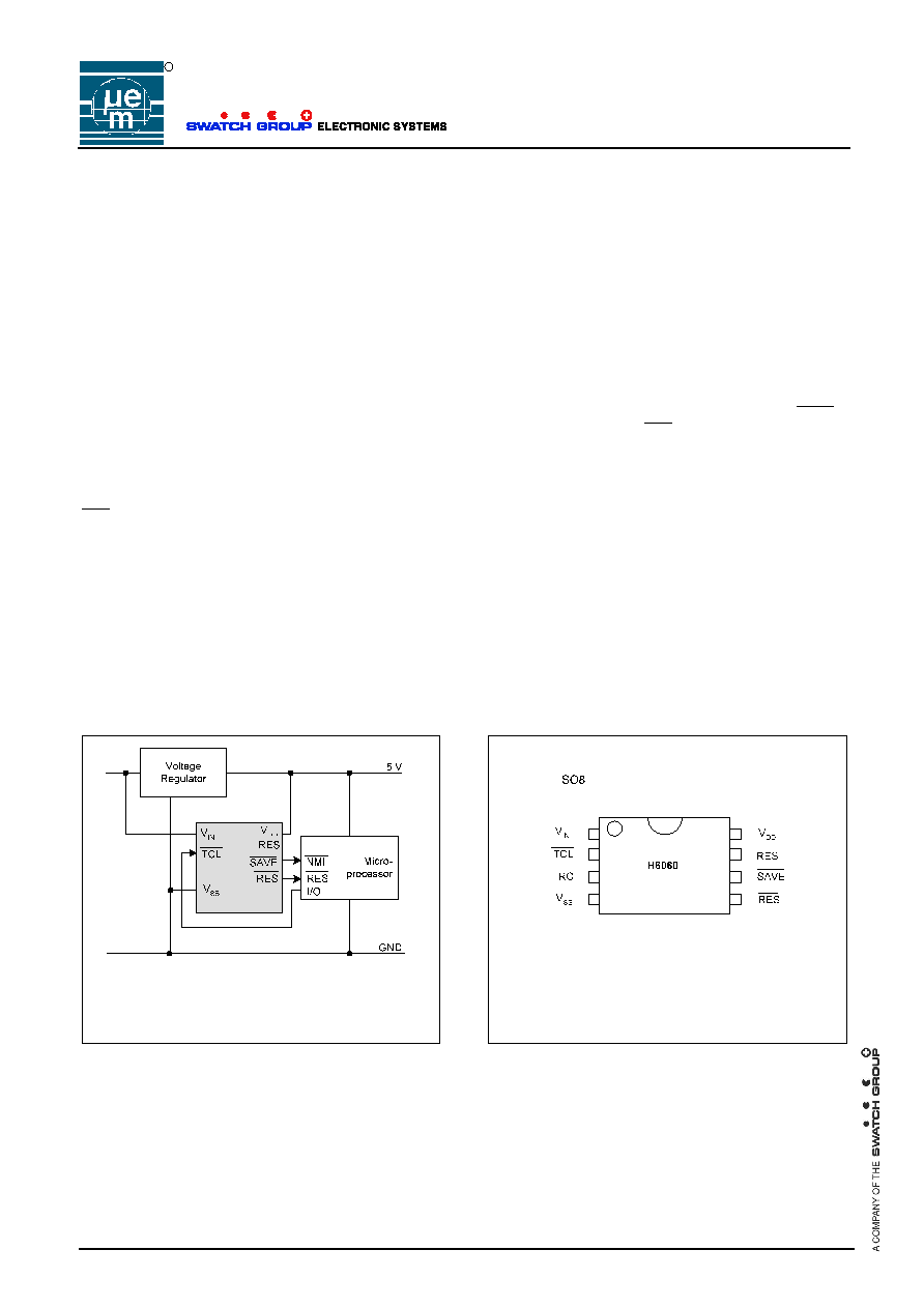
Typical Operating Configuration
H
6
060
Fig. 1
Pin Assignment
Fig. 2
EM MICROELECTRONIC -
MARIN SA
R
H6060
Copyright © 2004, EM Microelectronic-Marin SA
2
www.emmicroelectronic.com
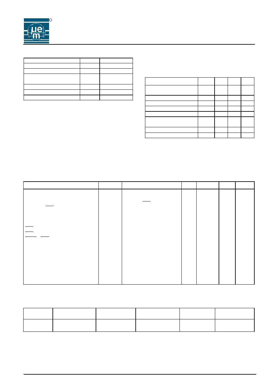
Absolute Maximum Ratings
Parameter Symbol
Conditions
Voltage V
DD
to V
SS
V
DD
- 0.3 to + 8 V
Voltage at any pin to V
SS
V
MIN
- 0.3
Voltage at any pin to V
DD
(except V
IN
)
V
INMAX
+
0.3
Voltage at V
IN
to V
SS
V
MIN
+ 15 V
Current at any output
I
MAX
± 10 mA
Storage temperature
T
STO
-65∞C to +150∞C
Table 1
Stresses above these listed maximum ratings may cause
permanent damages to the device. Exposure beyond
specified operating conditions may affect device reliability
or cause malfunction.
Handling Procedures
This device has built-in protection against high static
voltages or electric fields; however, anti-static precautions
must be taken as for any other CMOS component. Unless
otherwise specified, proper operation can only occur when
all terminal voltages are kept within the voltage range.
Unused inputs must always be tied to a defined logic
voltage level.
Operating Conditions
Parameter Symbol
Min.
Max. Units
Operating temperature
Industrial
T
AI
-40
+85
∞C
Supply voltage
V
DD
1.6 5.5 V
Comparator input voltage
Version 13, 14, 15, 16
V
IN
0 V
DD
V
Version 11,12
V
IN
0 12 V
RC-oscillator programm-
ing (see Fig. 15)
External capacitance
C1 1
µF
External resistance
R1
10
k
Table 2
* Leakage < 1µA
Electrical Characteristics
V
DD
= 5.0 V, T
A
=
-40 to +85 ∞C, unless otherwise specified
Parameter Symbol
Test
Conditions
Min.
Typ.
Max.
Units
V
DD
activation threshold
V
DD
deactivation threshold
Supply current
Input V
IN
, TCL
Leakage current
Input current on pin V
IN
TCL
input low level
TCL
input high level
SAVE
, RES , RES outputs
Leakage currents
Drive currents (all versions)
Drive currents
(versions 14,16)
1)
V
ON
V
OFF
I
DD
I
IP
I
IN
V
IL
V
IH
I
OLK
I
OL
I
OL
I
OL
I
OH
I
OH
I
OH
T
A
= 25
∞C
T
A
= 25
∞C
RC open, TCL at V
DD
or V
SS
V
SS
V
IP
V
DD
;
T
A
= 85
∞C
Version 12; V
IN
= 10 V
Version 15;
V
OUT
= V
DD
V
OL
= 0.4 V
V
DD
= 3.5 V; V
OL
= 0.4 V
V
DD
= 1.6 V; V
OL
= 0.4 V
V
OH
= 4.0 V
V
DD
= 3.5 V; V
OH
= 2.8 V
V
DD
= 1.6 V; V
OH
= 1.2 V
3
2.4
3.2
2
80
3.2
2
80
V
ON
- 0.3
80
0.005
100
0.05
8
8
3.5
140
1
180
0.8
1
V
V
µA
µA
µA
V
V
µA
mA
mA
µA
mA
mA
µA
1) Versions: 15 = open drain outputs; 14, 16 = push-pull outputs
Table 3
V
IN
Surveillance
Voltage thresholds at T
A
= 25
∞C
Version
1)
Comparator
Reference
Input Resistance
on V
IN
(R
VIN
)
Threshold
V
SH
V
SL
V
RL
Thresholds
Tolerance
Ratio
Tolerance
3)
14 V
DD
100M
2.25 2.00 1.75
2)
±5%
±2%
15, 16
Band-gap reference
100M
2.00 1.95 1.90
±10%
±2%
1)
Version: 15 = open drain outputs; 14, 16 = push-pull outputs
2)
at V
DD
= 5 V
3)
Threshold ratio tolerance is defined as the tolerance of V
SH
/ V
SL
and V
SL
/ V
RL
.
Table 4

R
H6060
Copyright © 2004, EM Microelectronic-Marin SA
3
www.emmicroelectronic.com
Timing Characteristics
V
DD
= 5.0 V, T
A
=
-40 ∞C to +85 ∞C, unless otherwise specified
Parameter Symbol Test
Conditions Min.
Typ.
Max.
Units
Propagation delays
TCL
to output pins
V
IN
to output pins
Logic transition times on
all output pins
Timeout period
T
TCL
input pulse width
Power-on reset debounce
V
IN
low pulse
T
DIDO
T
AIDO
T
TR
T
TO
T
TO
T
TCL
T
DB
T
VINL
Excluding debounce time T
DB
Load 10 k
, 100 pF
RC open, unshielded, T
A
= 25
∞C
RC open, unshielded (not tested)
Where debounce time T
DB
Is guaranteed
60
45
150
10
250
4
30
100
T
TO
/64
500
10
100
160
200
ns
µs
ns
ms
ms
ns
ms
µs
Table
5
Timing Waveforms
Voltage Reaction: V
DD
Monitoring
Voltage Reaction: V
IN
Monitoring
V
DD
V
ON
V
OFF
V
IN
monitoring enabled
Fig. 3
V
IN
V
SH
V
SL
V
RL
0
SAVE
RES
RES
T
TO
T
DB
T
TO
T
DB
T
VINL
Conditions:
V
DD
> V
ON
.
No timeout.
Fig. 4
Timer
Start
Power-on Reset
Timer
Stop Timer
Start
Power-on Reset
No Power-on Reset
(as V
IN
> V
RL
)

R
H6060
Copyright © 2004, EM Microelectronic-Marin SA
4
www.emmicroelectronic.com
Timer Reaction
Combined Voltage and Timer Reaction
Block Diagram
V
IN
V
SH
V
SL
V
RL
SAVE
RES
RES
TCL
Initialisation
RES
RES
Timeout Recover
Timer
Reset
Timer
Stop
T
TO
T
TO
T
TO
T
DB
Fig. 6
V
DD
Band-Gap
Reference
Save
Control
Reset
Control
OSC
Timer
TCL
SAVE
RES
RES
V
IN
1
2
3
V
SH
V
SL
V
RL
V
SS
RC
+
+
+
+
Fig. 7
Version Connections
11, 12 1 and 3
13, 14 1
15, 16 2
RES
RES
S
TCL
Timeout
Timer
Reset
Timer
Reset
Timer
Reset
T
TO
T
TO
Fig. 5
T
TCL
T
TO
T
TO
Conditions:
V
IN
> V
RL
after
power-up sequence
R
H6060
Copyright © 2004, EM Microelectronic-Marin SA
5
www.emmicroelectronic.com
Pin Description
Pin Name Function
1
V
IN
Voltage sense input
2
TCL
Timer clear input signal
3
RC
RC oscillator tuning input
4
V
SS
GND terminal
5
RES
Active low reset output
6
SAVE
Save output
7
RES
Active high reset output
8
V
DD
Positive supply voltage terminal
Table
6
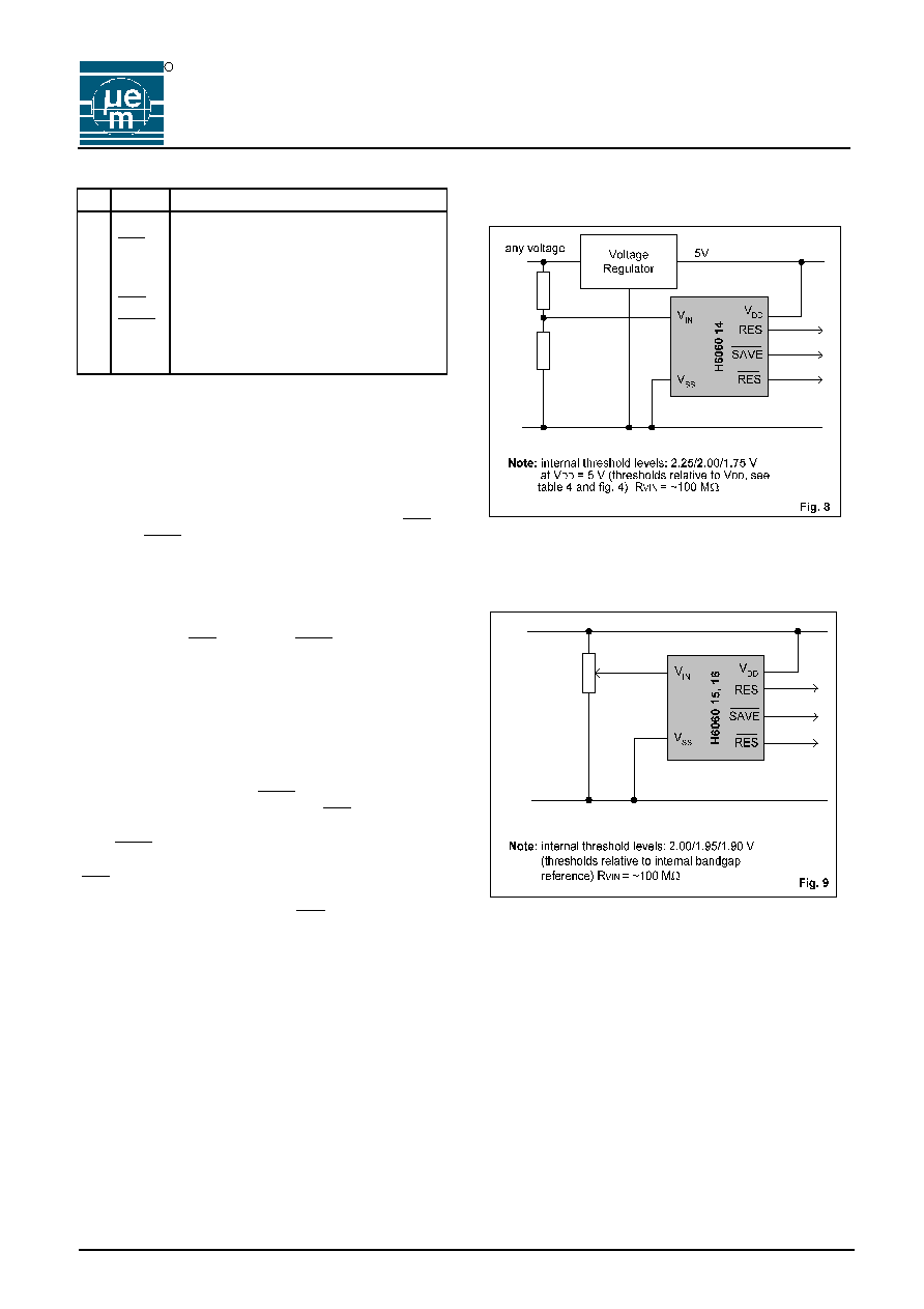
Functional Description
Supply Lines
The circuit is powered through the V
DD
and V
SS
pins. It
monitors both its own V
DD
supply and a voltage applied to
the V
IN
input.
V
DD
Monitoring
During power-up the V
IN
monitoring is disabled and RES ,
RES and SAVE stay active low as long as V
DD
is below
V
ON
(3.5 V). As soon as V
DD
reaches the V
ON
level, the
state of the outputs depend on the watchdog timer and
the voltage at V
IN
relative to the thresholds (see Fig. 4). If
the supply voltage V
DD
falls back below V
OFF
(V
ON
≠ 0.3 V)
the watchdog timer and the V
IN
monitoring are disabled
and the outputs RES , RES and SAVE become active.
The V
DD
line should be free of voltage spikes.
V
IN
Monitoring
The analog voltage comparators compare the voltage
applied to V
IN
(typically connected to the input of the
voltage regulator) with the stabilized supply voltage V
DD
(version 14) or with the bandgap voltage (versions 15, 16)
(see Fig. 7). At power-up, when V
DD
reached V
ON
and V
IN
reaches the V
SH
level, the SAVE output goes inactive,
and the timer starts running, setting RES and RES in
active after the time T
TO
(see. Fig. 4). If V
IN
falls below V
SL
, the SAVE output goes active and stays active until V
IN
rises again above V
SH
. If V
IN
falls below the voltage V
RL
,
RES
and RES will become active and the on-chip timer
will stop. When V
IN
rises again above V
SH
, the timer will
initiate a power-up sequence. The RES and RES outputs
may however be influenced independently of the voltage
V
IN
by the timer action, see section
Combined Voltage
and Timer Action". Monitoring the rough DC side of the
regulator, as shown in Fig. 11, is the only way to have
advanced warning of power-down. Spikes on V
IN
should
be filtered if they are likely to exceed the value (V
SL
≠
V
RL
).
The combination of V
IN
and V
DD
monitoring provide high
system security: if V
IN
rises much faster than V
DD
, then
the device starts the power-on sequence only when V
DD
reached V
ON
(Fig. 10). Short circuits on the regulated
supply voltage can be detected.
Voltage Thresholds on V
IN
The H6060 is available with 3 different sets of
thresholds:
Version 14: monitor the unregulated voltage and are
ideal for programming of the V
IN
voltage thresholds. Fixed
resistor values can be used for programming.
Version 15, 16: monitor the regulated voltage. They are
suited to applications where the unregulated voltage is
not available. (The tolerance is
± 10%, see table 4. For
tighter tolerances, trimming can be used, see Fig. 9).
Monitoring of the unregulated voltage requires version 14.
These versions are based on the principle that V
DD
rises
with V
IN
on power-up an V
DD
holds up for a certain time
after V
IN
starts dropping on power-down. The versions 11
and 12 have a 100 k
nominal resistance from V
IN
to V
SS
(internal voltage divider). The versions 14, 15 and 16
have high impedance V
IN
inputs (see Fig. 7 and Table 4)
for external threshold voltage programming by a voltage
divider on pin V
IN
. The levels obtained are proportional to
the internal levels V
SH
, V
SL
and V
RL
on the chip itself (see
Electrical Specifications).