
The V3021 is a low power CMOS real time clock. Data is
transmitted serially as 4 address bits and 8 data bits, over one
line of a standard parallel data bus. The device is accessed by
chip select (CS) with read and write control timing provided by
either RD and WR pulse (Intel CPU) or DS with advanced R/W
(Motorola CPU). Data can also be transmitted over a
conventional 3 wire serial interface having CLK, data I/O and
strobe. The V3021 has no busy states and there is no danger of
a clock update while accessing. Supply current is typically 800
nA at V = 3.0 V. Battery operation is supported by complete
DD
functionality down to 2.0 V. The oscillator stability is typically 0.3
ppm/V.
Applications
n Utility meters
Battery operated and portable equipment
Consumer electronics
White/brown goods
Pay phones
Cash registers
Personal computers
Programmable controller systems
Data loggers
Automotive electronics
n
n
n
n
n
n
n
n
n
1
Features
n Supply current typically 800 nA at 3 V
50 ns access time with 50 pF load capacitance
Fully operational from 2.0 V to 5.5 V
No busy states or danger of a clock update while
accessing
Serial communication on one line of a standard parallel
data bus or over a conventional 3 wire serial interface
Interface compatible with both Intel and Motorola
Seconds, minutes, hours, day of month, month, year, week
day and week number in BCD format
Leap year and week number correction
Time set lock mode to prevent unauthorized setting of the
current time or date
Oscillator stability 0.3 ppm / volt
No external capacitor needed
Frequency measurement and test modes
o
Temperature range - 40 to +85 C
Packages DIP8 and SO8
n
n
n
n
n
n
n
n
n
n
n
n
n
Description
Ultra Low Power 1-Bit 32 kHz RTC
Typical Operating Configuration
W
R
o
r
R
/
W
R
D
o
r
D
S
I/O
A
D
D
R
E
S
S
B
U
S
D
A
T
A
B
U
S
XI
XO
WR
WR
RD
RD
CS
CS
CPU
Address
Decoder
V3021
RAM
Fig. 1
Pin Assignment
XI
XO
CS
V
SS
DIP8 / SO8
V
DD
WR
RD
I/O
V3021
Fig. 2
EM MICROELECTRONIC-MARIN SA
R
V3021
Handling Procedures
Stresses above these listed maximum ratings may
cause permanent damage to the device. Exposure
beyond specified operating conditions may affect
device reliability or cause malfunction.
This device has built-in protection against high static voltages
or electric fields; however, it is advised that normal precautions
2
Absolute Maximum Ratings
Table 1
Parameter
Maximum voltage at V
DD
Minimum voltage at V
DD
Maximum voltage at any signal pin
Minimum voltage at any signal pin
Maximum storage temperature
Minimum storage temperature
Electrostatic discharge maximum
to MIL-STD-883C method 3015
Maximum soldering conditions
V
DDmax
V
DDmin
V
max
V
min
T
STOmax
T
STOmin
V
Smax
T
Smax
V
+ 7.0 V
SS
V
- 0.3 V
SS
V
- 0.3 V
SS
V
+ 0.3 V
DD
O
+150 C
O
-65 C
1000 V
O
250 C x 10 s
Symbol Conditions
Electrical Characteristics
O
V = 5.0V � 10%, V = 0 V and T = - 40 to 85 C, unless otherwise specified
DD
SS
A
Total static supply
Total static supply
Dynamic current
Input / Output
Input logic low
Input logic high
Output logic low
Output logic high
Input leakage
Output tri-state leakage
on I/O pin
Oscillator
Starting voltage
Input capacitance on XI
Output capacitance on XO
Start-up time
Frequency stability
Frequency Measurement Mode
Current source on I/O pin
pulsed on/off @ 256 Hz
I
SS
I
SS
I
SS
V
IL
V
IH
V
OL
V
OH
I
IN
I
TS
V
STA
C
IN
C
OUT
T
STA
D
f/f
I
ONF
all outputs open, all inputs at V
DD
V = 3.0 V, address 0 = 0
DD
3.5
0.8
1.8
m
A
m
A
m
A
m
A
V
V
V
V
m
A
m
A
V
pF
pF
s
ppm/V
m
A
10
3
300
1.0
0.4
1
1
0.5
60
1.3
0.1
0.1
13
9
1
0.3
25
2.4
1.8
10
all outputs open, all inputs at V
DD,
V = 5 V, address 0 = 0
DD
O
T = +25 C
A
O
T = +25 C
A
O
T = +25 C
A
O
2.0
�
V
�
5.5V , T = +25 C
DD A
Table 3
Parameter
Symbol
Test Conditions
Min.
Typ.
Max.
Units
CS high, addr.0, bit 0, high
V = 1 V
I/O
I = 4 mA
OL
I = 4 mA
OH
0.0 < V < 5.0 V
IN
CS high, and address 0,
bit 0, low
I/O to V through 1 M
W
SS
RD = V , WR = V ,
SS
DD
CS = 4 MHz
address 0 = 0, read all 0
be taken as for any other CMOS component. Unless otherwise
specified, proper operation can only occur when all terminal
voltages are kept within the supply voltage range. Unused
inputs must always be tied to a defined logic voltage level.
Operating Conditions
T
A
-40
2.0
5.0
+85
O
C
V
V/
m
s
nF
kHz
pF
k
W
5.5
6
30
50
100
32.768
8.2
35
7
V
DD
C
L
R
S
f
Table 2
1)
See Fig. 3
Parameter
Symbol Min. Typ . Max. Units
Operating temperature
Logic supply voltage
Supply voltage dv/dt
(power-up & power-down)
Decoupling capacitor
Crystal Characteristics
1)
Frequency
Load capacitance
Series resistance
R
V3021

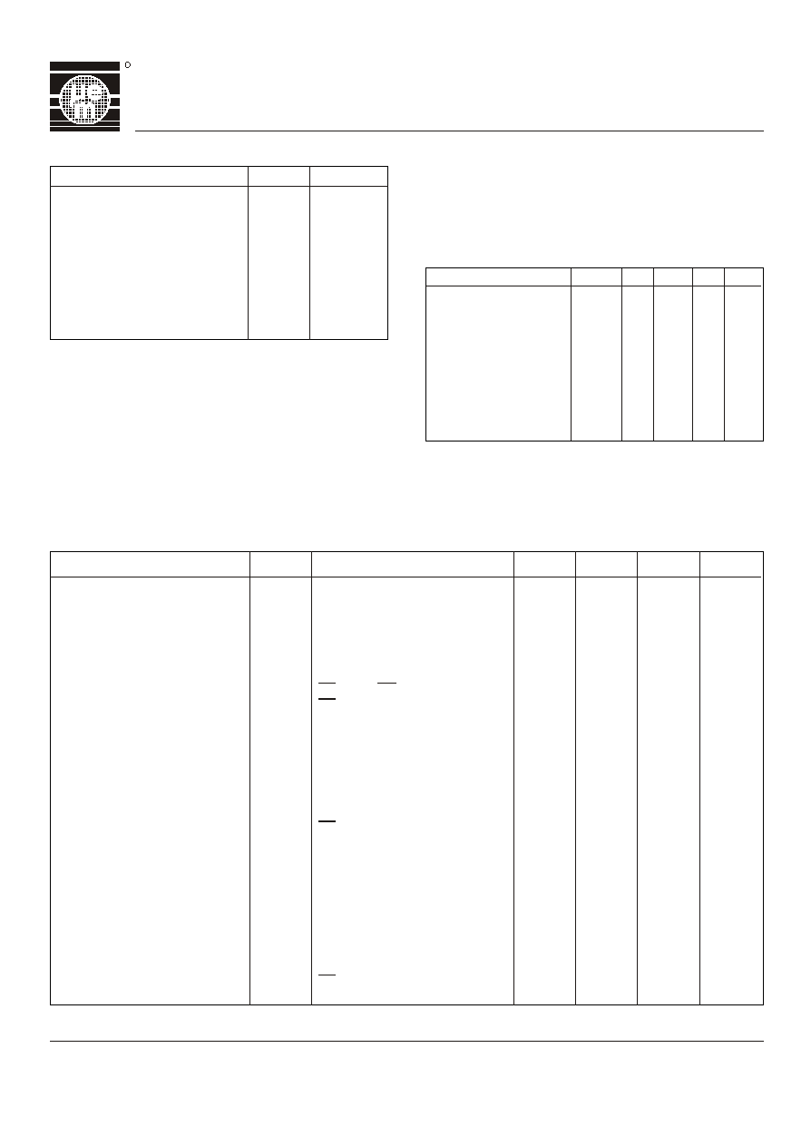
The V3021 will run slightly too fast, in order to allow the user to
adjust the frequency, depending on the mean operating
temperature. This is made since the crystal adjustment can only
work by lowering the frequency with an added capacitor
3
between XO and V . The printed circuit capacitance has also to
SS
be taken in consideration. The V3021 in DIL8 package, running
with an 8.2 pF crystal at room temperature, will be adjusted to
better than � 1 s/day with a 6.8 pF capacitor.
Typical Frequency on I/O Pin
80
30
-20
-70
-120
-170
[ppm]
3
2
1
0
-1
-2
s/day
Address 10 hex = 00 hex
Quartz with 8.2 pF load capacitance
External trimming capacitor between X and V [pF]
O
SS
O
T [ C]
A
Typical drift for ideal 32'768 Hz quartz
Note : The trimming capacitor value must not exceed 15 pF.
Greater values may disturb the oscillator function.
Fig. 3
-50
-30
-10
10
30
50
70
90
0
3
6
9
12
15
D
F
F
o
Quartz Characteristics
= the ratio of the change in frequency to the nominal value
expressed in ppm (It can be thought of as the frequency
deviation at any temperature.)
= the temperature of interest in C
O
= the turnover temperature (25 � 5 C)
O
To determine the clock error (accuracy) at a given temperature, add
O
the frequency tolerance at 25 C to the value obtained from the
formula above.
Fig. 4
[ppm]
-100
-200
-300
-400
T -100
O
T -50
O
O
Temperature [ C]
O
T [ C]
T
O
T +50
O
T +100
O
D
F
F
0
D
F
F
o
ppm
2
O
C
= - 0.038
2
(T - T ) �10%
O
D
F/F
o
T
T
O
m
in
.
m
ax
.
F
r
e
q
u
e
n
c
y
r
a
t
i
o
[
p
p
m
]
R
V3021
1)
t
starts from RD or CS, whichever activates last
ACC
Typically, t
= 5 + 0.9 C
in ns; where C
(external parasitic capacitance) is in pF
ACC
EXT
EXT
2)
CS, RD, DS, WR and R/W rise and fall times are specified by t and t
R
F
3)
t starts from RD or CS, whichever deactivates first
DF
4)
t
ends at WR or CS, whichever deactivates first
DW
5)
t starts from WR or CS, whichever deactivates first
DH
6)
t
starts from WR or CS, whichever activates last and ends at WR or CS, whichever deactivates first
WC
4
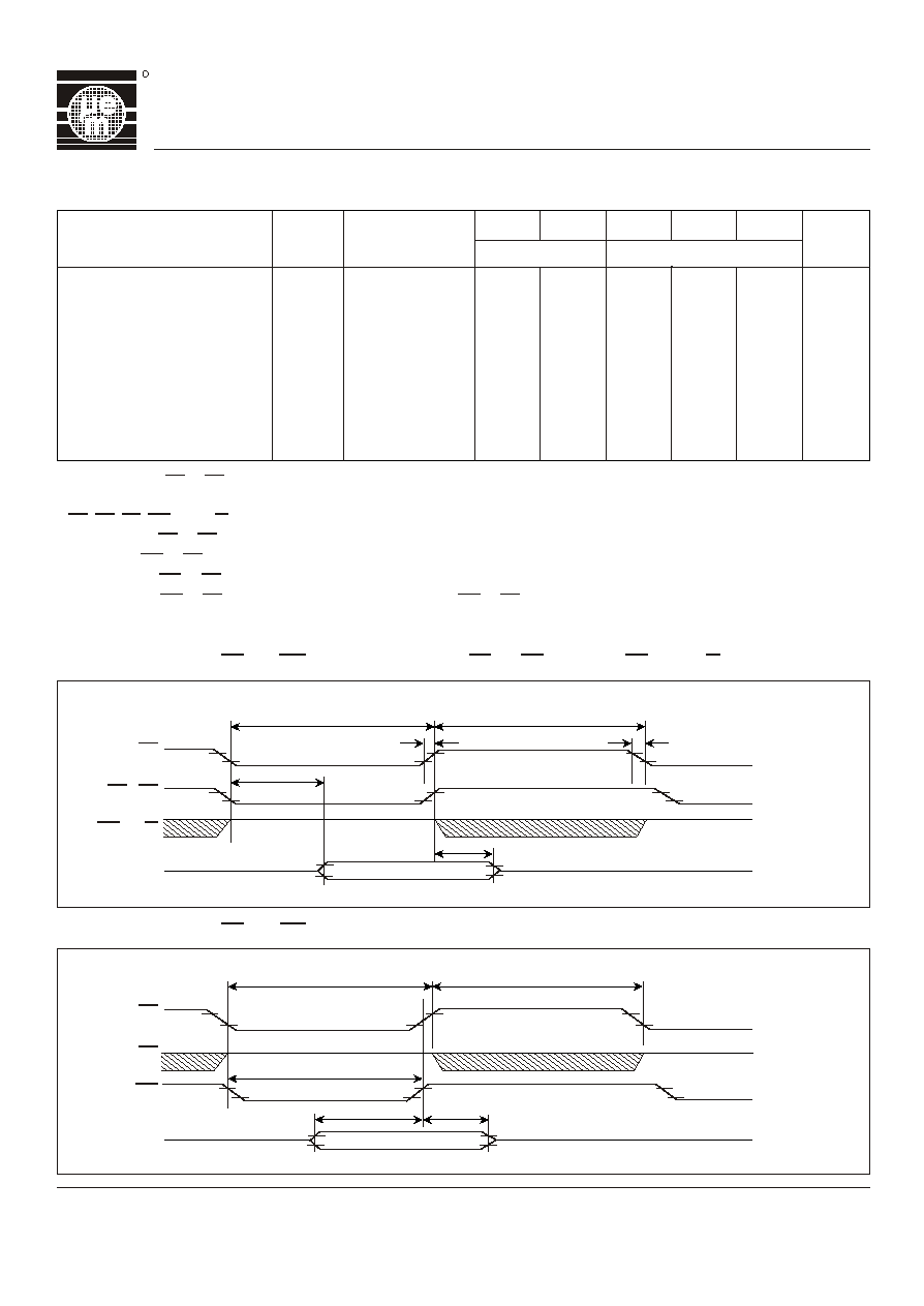
Timing Characteristics
O
V = 0 V, and T = - 40 to +85 C, unless otherwise specified
SS
A
Table 4
t
CS
t
ACC
t
W
t
R
t
F
t
DF
t
DW
t
DH
t
ADW
t
WC
200
500
10
10
10
60
80
25
200
50
100
10
10
15
50
25
10
50
ns
ns
ns
ns
ns
ns
ns
ns
ns
ns
60
200
200
40
50
30
180
200
200
100
Write cycle
C
= 50 pF
LOAD
Chip select duration
1)
RAM access time
Time between two transfers
2)
Rise time
2)
Fall time
3)
Data valid to Hi-impedance
4)
Write data settle time
5)
Data hold time
Advance write time
6)
Write pulse time
Parameter
Symbol
Test Conditions
Min.
Min.
Typ.
Max.
Max.
Units
V
�
2 V
DD
V = 5.0V � 10%
DD
Timing Waveforms
Read Timing for Intel (RD and WR Pulse) and Motorola (DS (or RD pin tied to CS) and R/W)
Fig. 5a
CS
t
CS
t
ACC
t
DF
t
W
t
R
t
F
RD / DS
WR / R/W
I/O
data valid
Write Timing for Intel (
and WR Pulse)
RD
R
V3021
Fig. 5b
CS
t
CS
t
W
t
WC
t
DW
t
DH
RD
WR
I/O
data valid
5
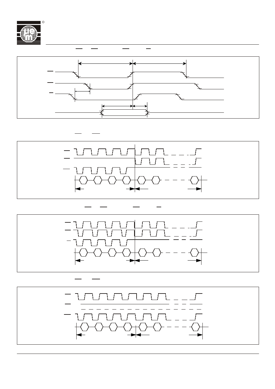
Communication Cycles
Read Data Cycle for Intel (RD and WR Pulse)
CS
RD " 1"
" 0"
WR
I/O
m
P writes 4 address bits
m
P reads 8 data bits
A0
A1
A2
A3
D0
D1
D7
Fig. 6c
Write Data Cycle for Intel (RD and WR Pulse)
CS
DS
R/W
I/O
m
P writes 4 address bits
m
P reads 8 data bits
A0
A1
A2
A3
D0
D1
D7
Fig. 6b
Read Data Cycle for Motorola (DS (or RD Pin Tied to CS) and R/W)
Write Timing for Motorola (DS (or RD pin tied to CS) and R/W)
CS
DS
R/W
I/O
t
ADW
t
DW
t
CS
t
W
t
DH
Fig. 5c
data valid
CS
DS
WR
I/O
m
P writes 4 address bits
m
P reads 8 data bits
A0
A1
A2
A3
D0
D1
D7
Fig. 6a
R
V3021