 | –≠–ª–µ–∫—Ç—Ä–æ–Ω–Ω—ã–π –∫–æ–º–ø–æ–Ω–µ–Ω—Ç: V6150 | –°–∫–∞—á–∞—Ç—å:  PDF PDF  ZIP ZIP |

EM MICROELECTRONIC--MARIN SA
V6150
1
Power Surveillance and Software Monitoring
Features
n
Standby mode, maximum current 45 mA
n
Reset output guaranteed for V
DD
voltage
down to 1.2 V
n
Comparator for voltage monitoring,
voltage reference 1.5 V
n
Programmable reset voltage monitoring
n
Programmable power-on reset (POR) delay
n
Watchdog with programmable time window
guarantees a minimum time and a maximum time
between software clearing of the watchdog
n
Time base accuracy ± 10
%
n
System enable (EN) output offers added security
n
TTL / CMOS compatible
n
-40 to +85 ∞C temperature range
n
On request extended temperature range,
-
40 to +125
∞
C
n
DIP8 and SO8 packages
Description
The V6150 offers a high level of integration by voltage
monitoring and software monitoring in an 8 lead
package. A comparator monitors the voltage applied at
the V
IN
input comparing it with an internal 1.5 V
reference. The power-on reset function is initialized after
V
IN
reaches 1.5 V and takes the reset output inactive
after T
POR
depending of external resistance. The reset
output goes active low when the V
IN
voltage is less than
1.5 V. The RES and EN outputs are guaranteed to be in
a correct state for a supply voltage as low as 1.2 V. The
watchdog function monitors software cycle time and
execution. If the software clears the watchdog too
quickly (incorrect cycle time) or too slowly (incorrect
execution), it will cause the system to be reset. The
system enable output prevents critical control functions
being activated until software has successfully cleared
the watchdog three times. Such a security could be
used to prevent motor controls being energized on
repeated resets of a faulty system.
Applications
n
Automotive systems
n
Cellular telephones
n
Security systems
n
Battery powered products
n
Industrial electronics
Typical Operating Configuration
Pin Assignment
R
V
SS
EN
TCL
V
IN
V
DD
Fig. 1
100 nF
V6150
RES
GND
Version 00:
Version 01:
DIP8 / SO8
V
DD
R
TCL
RES
EN
Fig. 2
V6150
V
SS
V
IN
NC

V6150
2
Absolute Maximum Ratings
Parameter
Symbol Conditions
Maximum voltage at V
DD
Minimum voltage at V
DD
Max. voltage at any signal pin
Min. voltage at any signal pin
Storage temperature
Electrostatic discharge max. to
MIL-STD-883C method 3015
Max. soldering conditions
V
DDmax
V
DDmin
V
MAX
V
MIN
T
STO
V
Smax
T
Smax
V
SS
+ 7 V
V
SS
-
0.3 V
V
DD
+ 0.3 V
V
SS
-
0.3 V
-65 to+150
∞
C
1000 V
250 ∞C x 10 s
Table 1
Stresses above these listed maximum ratings may cause
permanent damage to the device. Exposure beyond
specified operating conditions may affect device
reliability or cause malfunction.
Handling Procedures
This device has built-in protection against high static
voltages or electric fields; however, anti-static
precautions must be taken as for any other CMOS
component. Unless otherwise specified, proper
operation can only occur when all terminal voltages are
kept within the supply voltage range. Unused inputs
must always be tied to a defined logic voltage level.
Operating Conditions
Parameter
Symbol Min. Typ. Max. Units
s
Operating temperature
1)
Supply voltage
2)
& guaranteed
3)
Comparator input
voltage
RC-oscillator
programming
T
A
V
DD
V
DD
V
IN
R
-40
1.2
1.2
0
10
+125
5.5
V
DD
1000
∞
C
V
V
V
k
Table 2
1)
The maximum operating temperature is confirmed
by sampling at initial device qualification. In produc-
tion, all devices are tested at +85
∞
C. On request
devices tested at +125
∞
C can be supplied.
2)
A 100 nF decoupling capacitor is required on the
supply voltage V
DD
for stability.
3)
RES and EN (EN only for version 00) must be pulled
up externally to V
DD
even if they are unused.
(Note: RES and EN are used as inputs by EM test.)
Electrical Characteristics
V
DD
= 5 V
±
10%, C = 100 nF, T
A
= -40 to +85
∞
C, unless otherwise specified
Parameter
Symbol Test Conditions
Min.
Typ.
Max.
Units
Supply current in standby mode
Supply current
and
Output Low Voltage
(vers. 01)
Output High Voltage
and V
IN
Input Low Level
Input High Level
Leakage current input
V
IN
input resistance
Comparator reference
1)
Comparator hysteresis
1)
I
SS
I
SS
V
OL
V
OL
V
OL
V
OL
V
OH
V
OH
V
OH
V
IL
V
IH
I
LI
R
VIN
V
REF
V
REF
V
REF
V
HY
R
EXT
= don't care, TCL = V
DD
,
V
IN
= 0 V
R
EXT
= 100 k
, I/Ps at V
DD
,
O/Ps 1 M
to V
DD
V
DD
= 4.5 V, I
OL
= 20 mA
V
DD
= 4.5 V, I
OL
= 8 mA
V
DD
= 2.0 V, I
OL
= 4 mA
V
DD
= 1.2 V, I
OL
= 0.5 mA
V
DD
= 4.5 V, I
OH
=
-
1mA
V
DD
= 2.0 V, I
OH
=
-
100
µ
A
V
DD
= 1.2 V, I
OH
=
-
30
µ
A
V
SS
V
TCL
V
DD
V
DD
= 5 V,T
A
= +25
∞
C
V
DD
= 5 V
V
DD
= 5 V,
-
40
∞
C
T
A
+125
∞
C
3.5
1.8
1.0
V
SS
2.0
1.474
1.436
1.420
23
75
0.4
0.2
0.2
0.06
4.1
1.9
1.1
0.05
100
1.52
2
45
120
0.4
0.4
0.2
0.8
V
DD
1
1.566
1.620
1.620
µ
A
µ
A
V
V
V
V
V
V
V
V
V
µ
A
M
V
V
V
mV
Table3
1)
The comparator reference is the power-down reset threshold. The power-on reset threshold equals the comparator reference
voltage plus the comparator hysteresis (see Fig. 5).
RES
EN
EN
TCL
TCL
TCL
TCL
RES EN

V6150
3
I
SS
Standby versus Temperature at V
DD
= 5 V
Timing Characteristics
V
DD
= 5.0 V
±
3
%
, C = 100 nF, T
A
=
-
40 to
+
85
∞
C, unless otherwise specified
Parameter
Symbol
Test Conditions
Min.
Typ.
Max.
Units
Propagation delays:
to Output Pins
V
IN
sensitivity
Logic Transition Times on all Output Pins
Power-on Reset delay
Watchdog Time
Open Window Percentage
Closed Window Time
Open Window Time
Watchdog Reset Pulse
T
CL
Input Pulse Width
T
DIDO
T
SEN
T
TR
T
POR
T
WD
OWP
T
CW
T
CW
T
OW
T
OW
T
WDR
T
WDR
T
TCL
Load 10 k
, 50 pF
R
EXT
= 123 k
,
±
1%
R
EXT
= 123 k
,
±
1%
R
EXT
= 123 k
,
±
1%
R
EXT
= 123 k
,
±
1%
R
EXT
= 123 k
,
±
1%
1
90
90
72
36
150
250
5
30
100
100
±
0.2 T
WD
0.8 T
WD
80
0.4 T
WD
40
T
WD
/ 40
2.5
500
20
100
110
110
88
44
ns
µ
s
ns
ms
ms
ms
ms
ms
ns
Table 4
Timing Waveforms
Watchdog Timeout Period
TCL
T
WD
= T
POR
T
CW
≠ closed window
T
OW
≠ open window
Watchdog
timer reset
Condition:
R
EXT
= 123 k
-
OWP
-
20%
+ OWP
+ 20%
80
100
120
Fig. 4
t [ms]
10
12
14
16
38
18
20
24
22
26
28
30
I
SS
[
µ
A]
-
10
0
-
20
-
30
-
40
10
20
30
40
50
60
70
80
T
A
[
∞
C]
Fig. 3
32
34
36
40
V6150
4
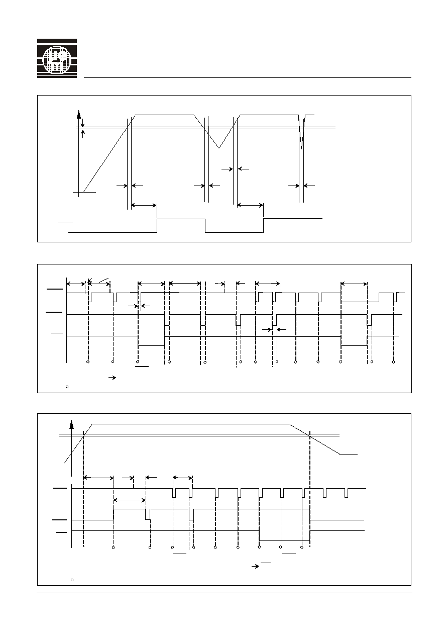
Voltage Monitoring
Timer Reaction
Combined Voltage and Timer Reaction
V
IN
Conditions:
V
DD
3V
Fig. 5
RES
No timeout
T
POR
V
REF
V
HY
T
SEN
T
SEN
T
SEN
T
SEN
T
POR
T
CW
+T
OW
T
POR
=T
WD
T
OW
T
CW
V
IN
V
REF
Condition:
V
DD
3 V
Fig. 7
TCL
TCL
RES
EN
too early
3 correct TCL service
EN goes active low
- Watchdog timer reset
1
2
3
T
TCL
T
OW
Fig. 6
- Watchdog timer reset
Conditions: V
IN
>
V
REF
after power-up sequence
TCL
RES
EN
EN
3 correct TCL services
goes active low
1
2
3
Timeout
T
CW
+T
OW
T
CW
T
CW
+T
OW
T
CW
T
CW
+T
OW
T
CW
T
OW
T
WDR
V6150
5
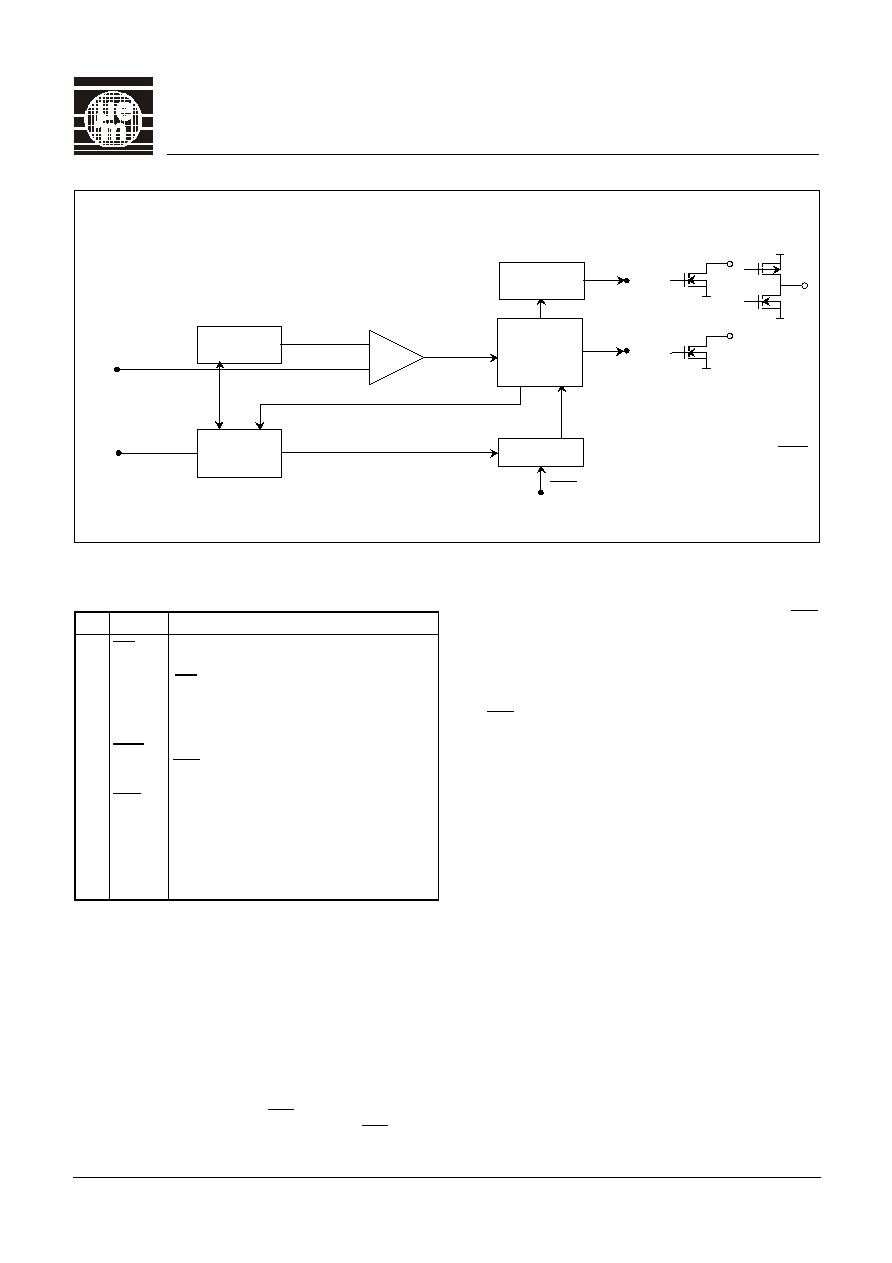
Block Diagram
Pin Description
Pin Name
Function
1
2
3
4
5
6
7
8
V
SS
NC
V
DD
R
V
IN
Vers. 00:
Open drain active low enable output.
must be pulled up to V
DD
even
if unused.
Vers. 01:
Push-pull active low enable output
Open drain active low reset output.
RES must be pulled up to V
DD
even
if unused
Watchdog timer clear input signal
GND terminal
No connection
Voltage supply
R
EXT
input for RC oscillator tuning
Voltage comparator input
Table 5
Functional Description
V
IN
Monitoring
The power-on reset and the power-down reset are
generated as a response to the external voltage level on
the V
IN
input. The external voltage level is typically
obtained from a voltage divider as shown in Fig. 9. The
user defines the external voltage divider to set the
desired threshold level for power-on reset and power-
down reset in his system. The internal comparator
reference voltage is typically 1.52 V.
At power-up the reset output (RES)
is held low (see Fig.
5). When V
IN
becomes greater than V
REF
, the RES output
is held low for an additional power-on reset (POR) delay
which is equal to the watchdog time T
WD
(typically 100
ms with an external resistor of 123 kW connected at R
pin). The POR delay prevents repeated toggling of RES
even if V
IN
and the INPUT voltage drops out and
recovers. The POR delay allows the microprocessor's
crystal oscillator time to start and stabilize and ensures
correct recognition of the reset signal to the
microprocessor.
The RES output goes active low generating the power-
down reset whenever V
IN
falls below V
REF
. The sensitivity
or reaction time of the internal comparator to the voltage
level on V
IN
is typically 5 ms.
Timer Programming
The on-chip oscillator with an external resistor R
EXT
connected between the R pin and V
SS
(see Fig.
9)
allows the user to
adjust the power-on reset (POR)
delay, watchdog time T
WD
and with this also the closed
and open time windows as well as the watchdog reset
pulse width (T
WD
/40).
With R
EXT
= 123 kW, the typical delays are:
- Power-on reset delay: T
POR
is 100 ms
- Watchdog time:
T
WD
is 100 ms
- Closed window:
T
CW
is 80 ms
- Open window:
T
OW
is 40 ms
- Watchdog reset:
T
WDR
is 2.5 ms
Note the current consumption increases as the frequen-
cy increases.
Watchdog Timeout Period Description
The watchdog timeout period is divided into two parts, a
"closed" window and an "open" window (see
Fig. 4) and
is
defined by two parameters, T
WD
and the Open Window
Percentage (OWP).
The closed window starts just after the watchdog timer
resets and is defined by T
CW
= T
WD
-
OWP(T
WD
).
EN
RES
TCL
EN
RES
EN
TCL
Fig. 8
V
REF
R
V
IN
Open drain
output RES
Current
Controlled
Oscillator
Voltage
Reference
Enable
Logic
Timer
Reset
Control
-
Comparator
Vers.00
Vers.01
+
V6150
6
The open window starts after the closed time window
finishes and lasts till T
WD
+ OWP(T
WD
). The open window
time is defined by T
OW
= 2 x OWP(T
WD
).
For example if T
WD
= 100 ms (actual value) and OWP =
±
20% this means the closed window lasts during first
the 80 ms (T
CW
= 80 ms = 100 ms
-
0.2 (100 ms)) and
the open window the next 40 ms (T
OW
= 2 x 0.2 (100 ms)
= 40 ms). The watchdog can be serviced between 80
ms and 120 ms after the timer reset. However as the
time base is
±
10% accurate, software must use the
following calculation as the limits for servicing signal
TCL during the open window:
Related to curves (Fig. 10 to Fig. 20), especially Fig. 19
and Fig. 20, the relation between T
WD
and R
EXT
could
easily be defined. Let us take an example describing the
variations due to production and temperature:
1. Choice, T
WD
= 26 ms.
2. Related to Fig. 20, the coefficient (T
WD
to R
EXT
) is 1.155
where R
EXT
is in kW and T
WD
in ms.
3. R
EXT
(typ.) = 26 x 1.155 = 30.0 kW.
4. 26 ms at +25
∞
C
a)
(26 - 10% = 23.4 ms) (26 + 10% = 28.6 ms)
a)
b)
(23.4 - 5% = 22.2 ms) (28.6 + 5% = 30.0 ms)
b)
min.: (30.0 - 20% = 24.0 ms) max.: (22.2 + 20% = 26.7 ms)
Typical TCL period of
(24.0 + 26.7) / 2 = 25.4 ms
The ratio between T
WD
= 26 ms and the (TCL
period)= 25.4 ms is 0.975.
Then the relation over the production and the full
temperature range is, TCL period = 0.975 x T
WD
or
TCL period = , as typical value.
a) While PRODUCTION value unknown for the custo-
mer when R
EXT
π 123 kW.
b) While operating TEMPERATURE range
-40 ∞C
T
A
+85 ∞C.
5. If you fixed a TCL period = 26 ms
ÞR
EXT
= 30.8 kW.
If during your production the T
WD
time can be measur-
ed at T
A
= +25 ∞C and the mC can adjust the TCL
period, then
the TCL period range will be much larger
for the full operating temperature.
Timer Clearing and RES Action
The watchdog circuit monitors the activity of the
processor. If the user's software does not send a pulse
to the TCL input within the programmed open window
timeout period, a short watchdog RES pulse is
generated which is equal to T
WD
/40 = 2.5 ms typically
(see Fig. 6).
With the open window constraint, new security is added
to conventional watchdogs by monitoring both software
cycle time and execution. Should software clear the
watchdog too quickly (incorrect cycle time) or too slowly
(incorrect execution), it will cause the system to be reset.
If the software is stuck in a loop which includes the
routine to clear the watchdog, then a conventional
watchdog would not make a system even though the
software is malfunctioning; the V6150 would make a
system reset because the watchdog would be cleared
too quickly.
If no TCL pulse is applied before the closed and open
windows expire, RES will start to generate square waves
of period
-
T
CW
+ T
OW
+ T
WDR
. The watchdog will remain
in this state until the next TCL falling edge appears
during an open window, or until a fresh power-up
sequence. The system enable output, EN, can be used
to prevent critical control
functions being activated in the
event of the system going into this failure mode (see
section "Enable - EN Output").
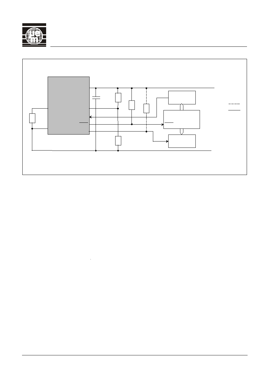
The RES output must be pulled up to V
DD
even if the
output is not used by the system (see Fig. 9).
Combined Voltage and Timer Action
The combination of voltage and timer actions is
illustrated by the sequence of events shown in Fig. 7. On
power-up, when the voltage at V
IN
reaches V
REF
, the
power-on-reset, POR, delay is initialized and holds RES
active for the time of the POR delay. A TCL pulse will
have no effect until this power-on-reset delay is
completed. After the POR delay has elapsed, RES goes
inactive and the watchdog timer starts acting. If no TCL
pulse occurs, RES goes active low for a short time T
WDR
after each closed and open window period. A TCL pulse
coming during the open window clears the watchdog
timer. When the TCL pulse occurs too early (during the
closed window), RES goes active and a new timeout
sequence starts. A voltage drop below the V
REF
level for
longer than
typically 5 ms, overrides the timer and
immediately forces RES active and EN inactive. Any
further TCL pulse has no effect until the next power-up
sequence has completed.
Enable -
- EN Output
The system enable output, EN, is inactive always when
RES is active and remains inactive after a RES pulse
until the watchdog is serviced correctly 3 consecutive
times (ie. the TCL pulse must come in the open
window). After three consecutive services of the
watchdog
with TCL during the open window, the EN
goes active low.
A malfunctioning system would be repeatedly reset by
the watchdog. In a conventional system critical motor
controls could be energized each time reset goes
inactive (time allowed for the system to restart) and in
this way the electrical motors driven by the system could
function out of control. The V6150 prevents the above
failure mode by using the EN output to disable the motor
controls until software has successfully cleared the
watchdog three times (i.e. the system has correctly
restarted after a reset condition).
For the version 00 the EN output must be pulled up to
V
DD
even if the output is not used by the system (see
Fig.9).
0.975 x R
EXT
1.155
26 x 1.155
0.975
V6150
7
Typical Application
R
V
SS
EN
TCL
V
IN
V
DD
GND
Fig. 9
100 nF
V6150
RES
RES
EN Motor
Controls
Address
Decoder
100 k
R1
R2
µ
P
Supply voltage
100 k
100 k
Version 00:
Version 01:
V6150
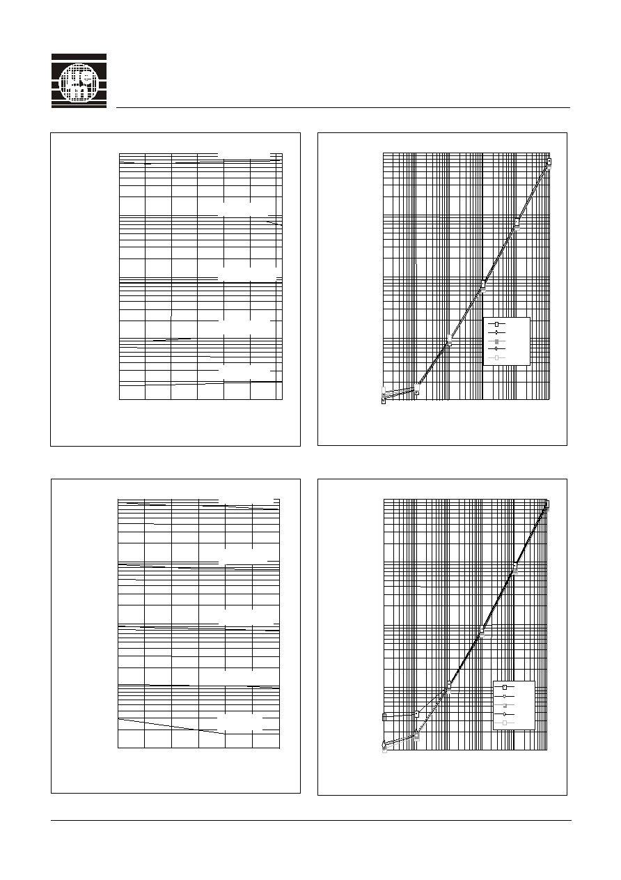
8
T
WD
versus Temperature at 5 V
T
WD
versus V
DD
at T
A
= +25
∞∞
C
T
WD
versus R at 5 V
T
WD
versus R at T
A
= +25
∞∞
C
+
80
Fig. 10
-
40
-
20
+
20
T
A
[
∞
C]
10'000
1000
100
10
1
T
WD
[ms]
0
+
40
+
60
R = 1 k
R = 1 M
R = 10 M
R = 100 k
R = 10 k
1
0.1
10'000
1000
100
10
10'000
1000
100
10
1
T
WD
[ms]
R [k
]
Fig. 11
-
40
∞
C
-
20
∞
C
+
25
∞
C
+
70
∞
C
+
85
∞
C
1
0.1
10'000
1000
100
10
10'000
1000
100
10
1
T
WD
[ms]
R [k
]
Fig. 13
3 V
4.8 V
5 V
5.2 V
6 V
6
Fig. 12
3
V
DD
[V]
10'000
1000
100
10
1
T
WD
[ms]
4
5
R = 1 k
R = 1 M
R = 10 M
R = 100 k
R = 10 k
V6150
9
T
WD
versus R at T
A
= +25
∞∞
C
1
0.1
10'000
1000
100
10
10'000
1000
100
10
1
T
WD
[ms]
R [k
]
Fig. 14
3 V
4.8 V
5 V
5.2 V
6 V
V6150
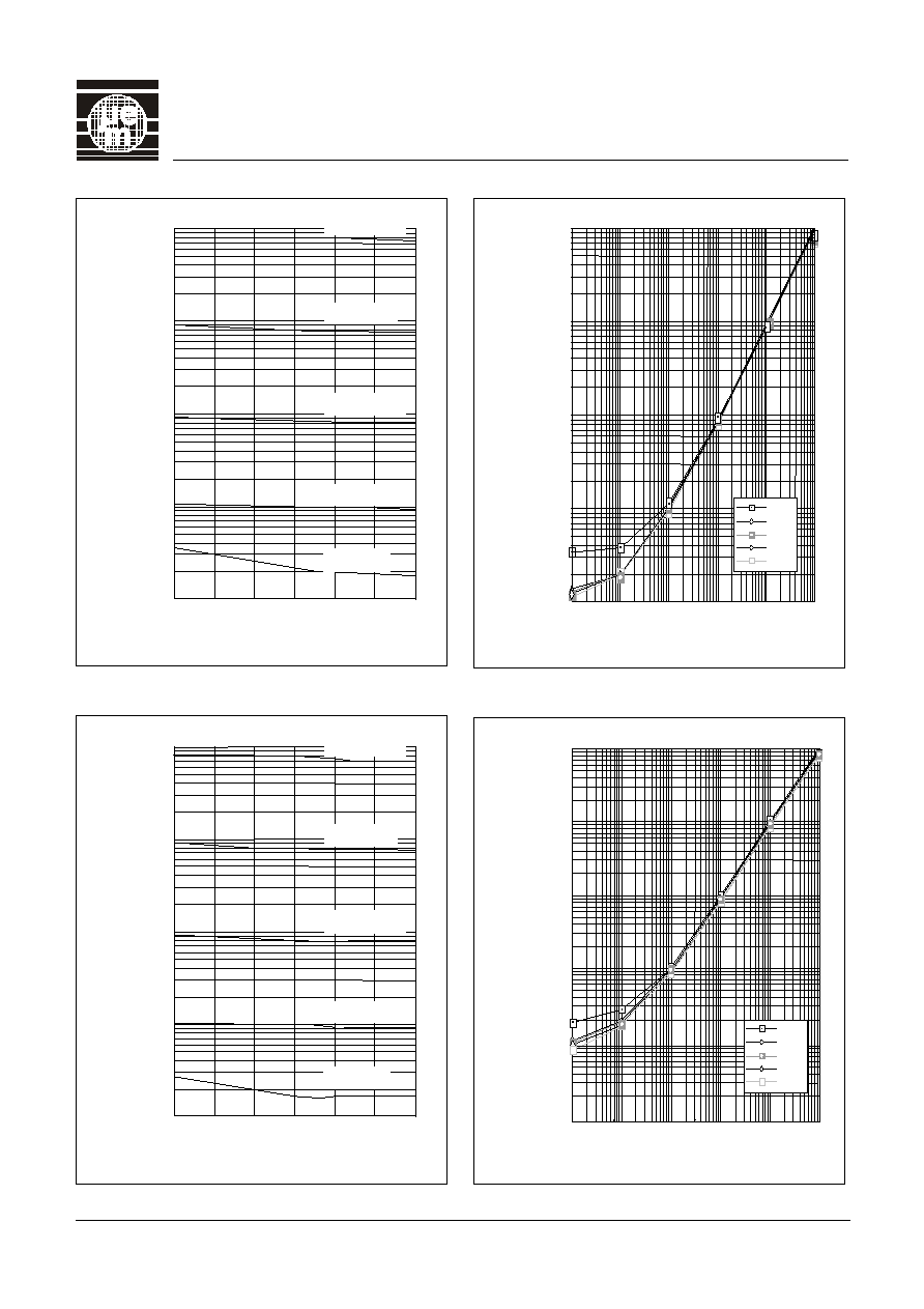
10
T
WD
versus V
DD
at T
A
= +85
∞∞
C
T
WD
versus V
DD
at T
A
=
--
40
∞∞
C
T
WD
versus R at T
A
= +85
∞∞
C
T
WD
versus R at T
A
=
--
40
∞∞
C
6
Fig. 17
3
V
DD
[V]
10'000
1000
100
10
1
T
WD
[ms]
4
5
R = 10 M
R = 1 M
R = 100 k
R = 10 k
R = 1 k
6
Fig. 15
3
V
DD
[V]
10'000
1000
100
10
1
T
WD
[ms]
4
5
R = 1 k
R = 1 M
R = 10 M
R = 100 k
R = 10 k
1
0.1
10'000
1000
100
10
10'000
1000
100
10
1
T
WD
[ms]
R [k
]
Fig. 16
3 V
4.8 V
5 V
5.2 V
6 V
1
0.1
10'000
1000
100
10
0.1
1000
100
10
1
T
WD
[ms]
R [k
]
Fig. 18
3 V
4.8 V
5 V
5.2 V
6 V

V6150
11
T
WD
Coefficient versus R
EXT
at T
A
= +25
∞∞
C
R
EXT
Coefficient versus T
WD
at T
A
= +25
∞∞
C
0.96
0.94
0.92
0.90
0.88
0.86
0.84
0.82
0.80
0.78
0.76
T
WD
Coefficient
10
1000
100
R
EXT
[k
]
Fig. 19
Fig. 20
1.30
1.28
1.26
1.24
1.22
1.20
1.18
1.16
1.14
1.12
1.10
1.08
1.06
1.04
R
EXT
Coefficient
10
100
1000
T
WD
[ms]

V6150
12
Ordering Information
The V6150 is available in the following packages:
Industrial temperature range (
-
40 to +85
∞
C)
Type
1)
Package
V6150 nn 8P
DIP8
V6150 nn 8S
SO8
When ordering please specify complete part number.
Marking on package:
Package
Marking
1)
DIP8
V6150 nn
SO8
6150 nn
1)
nn stands for the versions 00*,01
* on request
Extended temperature range (
-
40 to +125
∞
C)
Type
1)
Package
V6150 nn X 8P
DIP8*
V6150 nn X 8S SO8*
© 2000 EM Microelectronic-Marin SA, 10/00, Rev. D/314
EM Microelectronic-Marin SA cannot assume any responsibility for use of any circuitry described other than entirely
embodied in an EM Microelectronic-Marin SA product. EM Microelectronic-Marin SA reserves the right to change the
circuitry and specifications without notice at any time. You are strongly urged to ensure that the information given
has not been superseded by a more up-to-date version.
EM Microelectronic-Marin SA, CH - 2074 Marin, Switzerland, Tel. (+41) 32 - 755 51 11, Fax (+41) 32 - 755 54 03