 | –≠–ª–µ–∫—Ç—Ä–æ–Ω–Ω—ã–π –∫–æ–º–ø–æ–Ω–µ–Ω—Ç: V6175 | –°–∫–∞—á–∞—Ç—å:  PDF PDF  ZIP ZIP |
Watchdog with Switch-Over
Features
Sleep mode maximum consumption: 500 nA at 3 V
Standby mode maximum current 38 µA
Reset output guaranteed for V
DD
down to 1.2 V
Comparator for voltage monitoring, reset threshold
1.275 V
± 2.0 % voltage reference accuracy at +25 ∞C
± 2.7 % voltage reference accuracy from -40 to +85
∞C
Time base accuracy ± 15 %
Programmable time window guarantees a minimum
and a maximum time between software clearing of
the watchdog
Automatic switching between main power supply and
battery supply
Switch over output is available to supply other
devices up to 100 mA under main supply
System enable (EN) output offers added security
TTL and CMOS compatible
DIP14, SO-14 and TSSO16 packages
Description
The V6175 is a high performance power supply and soft-
ware monitoring device. The supply voltage is monitored
by an external voltage divider which is connected to the
voltage comparator (V
IN
). When V
IN
is higher than the in-
ternal voltage reference (1.275 V), the RESET open-drain
output is controlled by the software monitoring. If V
IN
falls
below the threshold voltage, the Reset output is active to
low.
The push-pull EN output is inactive as long as the soft-
ware being monitored is operating correctly and that V
IN
is higher than the threshold voltage.
The software monitor is made by checking a signal of the
microprocessor which must give pulses in a valid time
window. This signal is connected to the watchdog
through the TCL input. The time window is controlled by
an external resistor, so that it can be adjusted by the user.
The internal switchover is used to supply the watchdog
and an external device such as a user RAM. When the
main power supply is switched off, the RAM and the
watchdog are supplied by the battery.
The V6175A version 05 has a system enable output which
prevents critical control functions being activated until
software has successfully cleared the watchdog three
times. Such a security could be used to prevent motor
controls being energized on repeated resets of a faulty
system.
The version 15 offers a sleep mode function interesting
for safety current. It has 4 different modes of functionality:
watchdog mode, main supply monitoring mode, battery
level monitoring mode and sleep mode. This mode has a
typical current consumption of 500 nA. To have an expla-
nation of the functionality for the different modes, see
page 7 .
Applications
Industrial and automotive electronics
Cellular telephones
Security system
Automotive electronics
Battery powered products
1
V6175
EM MICROELECTRONIC-MARIN SA
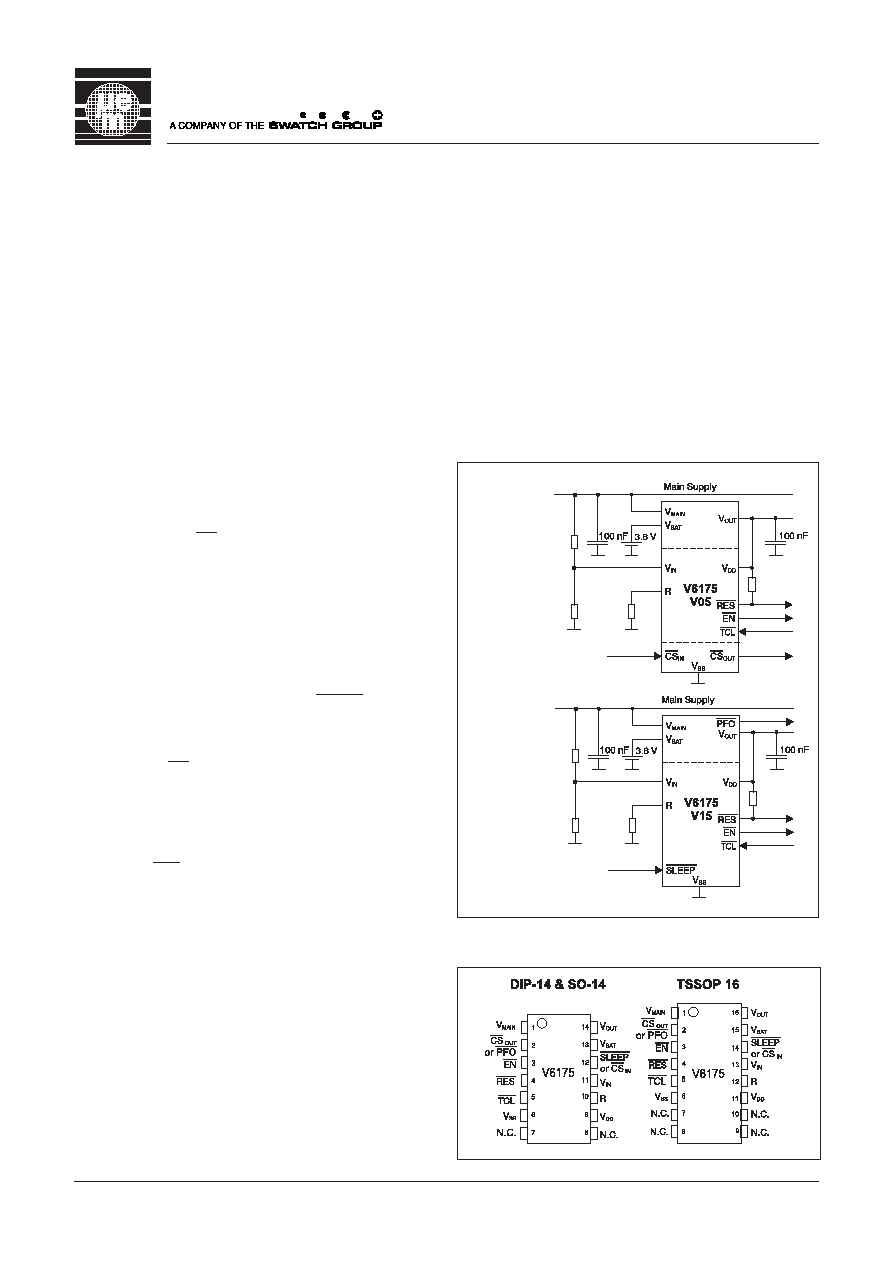
Typical Operating Configuration
Pin Assignment
Fig. 2
Fig. 1
Version 05
Version 15

Absolute Maximum Ratings
Parameter
Symbol
Conditions
Max. voltage at V
MAIN
, V
BAT
V
SUPmax
V
SS
+ 7 V
and V
DD
Max. Voltage at any signal pin
V
MAX
V
DD
+ 0.3 V
Min. Voltage at any pin
V
MIN
V
SS
- 0.3 V
Storage temperature range
T
STO
-65 to +150 ∞C
Electrostatic discharge max.
V
Smax
1000 V
to MIL-STD-883C method 3015
Max. soldering conditions
T
Smax
250 ∞C x10s
Table 1
Stresses above these listed maximum ratings may cause
permanent damage to the device. Exposure beyond
specified operating conditions may affect device reliabil-
ity or cause malfunction.
Handling Procedure
This device has built-in protections against high static
voltages or electric fields; however, anti-static precau-
tions must be taken as for any other CMOS component.
Unless otherwise specified, proper operation can only
occur when all terminal voltages are kept within the al-
lowed voltage range.
Operating Conditions
Parameter
Symbol Min. Max. Unit
Operating temperature
T
A
-40
+85
∞C
Main supply voltage
V
MAIN
2
5.5
V
Battery supply voltage
V
BAT
2
4.0
V
Positive supply voltages
1)
V
DD
1.2
5.5
V
RES & EN guaranteed
2)
V
DD
1.2
V
Comparator input voltage
V
IN
0
V
DD
V
RC oscillator programming
3)
R
0.01
1
M
W
Table 2
1)
A 100 nF decoupling capacitor is required on the supply
voltage V
DD
for stability.
2)
RES must be pulled up externally to V
DD
even if it is unused.
(Note: RES and EN are used as inputs by EM test.)
3)
See Fig. 18 and 19.
2
V6175
Electrical Characteristics
3
£ V
DD
£ 5.5 V, V
MAIN
= 0 V, V
BAT
= 3 V, C = 100 nF, T
A
= -40 to +85 ∞C, unless otherwise specified
Parameter
Symbol Test Conditions
Min.
Typ.
Max.
Unit
Sleep mode current
I
SS
V
DD
connected to V
OUT
, V
MAIN
= 0 V,
170
500
nA
(only for version 15)
V
BAT
= 3 V, Sleep = 0,
R
EXT
= don't care, TCL = V
DD
,
V
IN
= 0V
Supply current in standby mode
I
SS
R
EXT
= don't care, TCL = V
DD
,
27
38
µA
V
IN
= 0 V
Supply current
I
SS
R
EXT
= 100 k
W, I/Ps at V
DD
,
55
100
µA
O/Ps 1 M
W to V
DD
RES, EN and CS
OUT
or PF
Output Low Voltage
V
OL
V
DD
= 4.5 V, I
OL
= 20 mA
0.4
V
V
OL
V
DD
= 4.5 V, I
OL
= 8 mA
0.2
0.4
V
V
OL
V
DD
=2.0 V, I
OL
= 4 mA
0.2
0.4
V
V
OL
V
DD
= 1.2 V, I
OL
= 0.5 mA
0.06
0.2
V
EN and CS
OUT
or PF
Output High Voltage
V
OH
V
DD
= 4.5 V, I
OH
= -1 mA
3.5
4.1
V
V
OH
V
DD
= 2.5 V, I
OH
= -100 µA
1.8
1.9
V
V
OH
V
DD
= 1.2 V, I
OH
= -30 µA
1.0
1.1
V
TCL and CS
IN
TCL and CS
IN
Input Low Level
V
IL
V
SS
0.8
V
TCL and CS
IN
Input High Level
V
IH
2.0
V
DD
V
Leakages
Current on signal inputs
I
LI
V
SS
£ inputs £ V
DD
0.05
1
µA
V
IN
input resistance
R
VIN
100
M
W
Current on RES
O
LI
V
SS
£ V
RES
£ V
DD
0.05
1
µA
Comparator reference
Threshold
1)
V
REF
T
A
= 25 ∞C
1.25
1.275
1.3
V
V
REF
1.24
1.31
V
Hysteresis
1)
V
HY
5
mV
Battery surveillance
(only for version 15)
Threshold
V
TBAT
V
DD
connected to V
OUT
2.75
2.85
2.95
V
Hysteresis
1)
V
HYBAT
V
MAIN
= 0 V
5
mV
Table 3
1)
The comparator reference is the power-down reset threshold. The power-on reset threshold equals the comparator reference
voltage plus the comparator hysteresis (see Fig. 6).
3
V6175
Timing Characteristics
V
DD
= 5 V ± 3%, C = 100 nF, T
A
= -40 to +85
o
C, unless otherwise specified
Parameter
Symbol Tests Conditions
Min.
Typ.
Max.
Unit
Propagation delays:
TCL to Output Pins
T
DIDO
250
500
ns
CS
IN
to CS
OUT
at rising edge
T
CSH
125
200
ns
CS
IN
to CS
OUT
at falling edge
T
CSL
75
150
ns
V
IN
sensitivity
T
SEN
1
5
20
µs
Logic Transition Times on all
T
TR
Load 10 k
W, 50 pF
30
100
ns
Output Pins
Power-on Reset delay
T
POR
R
EXT
= 110 k
W, ± 1%
68
80
92
ms
Watchdog Time
T
WD
R
EXT
= 110 k
W, ± 1%
68
80
92
ms
Open Window Percentage
OWP
±0.375T
WD
Closed Window Time
T
CW
0.625T
WD
T
CW
R
EXT
= 110 k
W, ± 1%
42.5
50
57.5
ms
Open Window Time
T
OW
0.75T
WD
T
OW
R
EXT
= 110 k
W, ± 1%
51
60
69
ms
Watchdog Reset Pulse
T
WDR
T
WD
/ 32
T
WDR
R
EXT
= 110kl
W. ± 1%
2.5
ms
T
TCL
Input Pulse Width
T
TCL
150
ns
Table 5
Timing Waveforms
Watchdog Timeout Period
Fig. 3
Switch-over Electrical Characteristics
T
A
= -40 to +85
o
C, unless otherwise specified
Parameter
Symbol Test Conditions
Min.
Typ.
Max.
Unit
ON resistance of V
MAIN
to V
OUT
R
MAIN
V
MAIN
= 3 V, V
BAT
= 0 V, I
OUT
= 100 mA
4
8
W
ON resistance of V
BAT
to V
OUT
R
BAT
V
MAIN
= 0 V, V
BAT
= 3 V, I
OUT
= 20 mA
10
40
W
V
MAIN
voltage over V
BAT
for switching
V
SMAIN
V
BAT
= 3 V, V
OUTPUT
open
3.00
3.21
3.45
V
V
MAIN
voltage under V
BAT
for switching V
BAT
V
BAT
= 3 V, V
OUTPUT
open
2.98
3.08
3.18
V
V
MAIN
rising edge switching delay to
T
RMAIN
V
BAT
= 3 V, V
MAIN
rise from 2.8 V to 3.5 V
14
100
µs
FO and V
OUT
V
MAIN
falling edge switching delay
T
FMAIN
V
BAT
= 3 V, V
MAIN
falling from 3.5 V to 2.8 V
8
60
µs
to PFO and V
OUT
Table 4
4
V6175
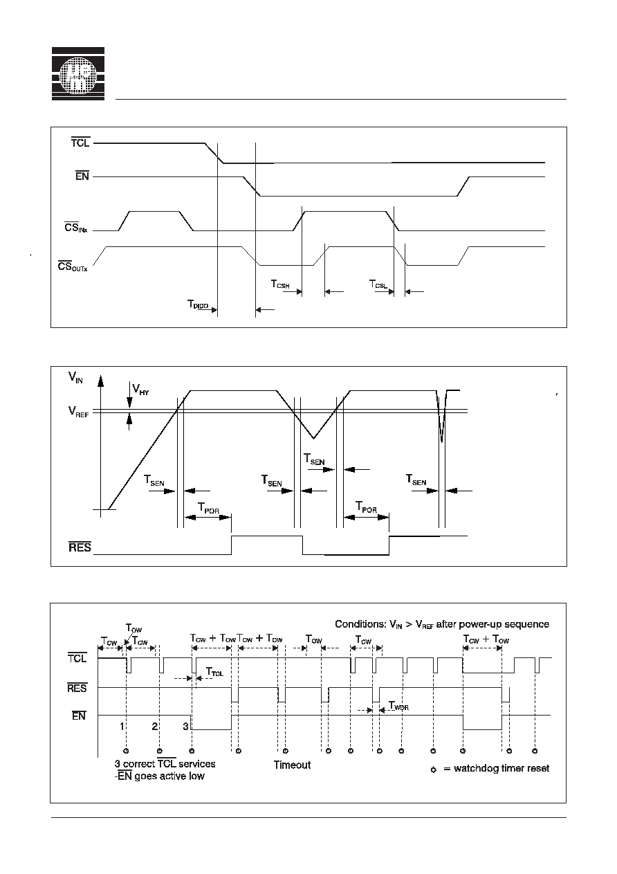
Chip Select
Voltage Monitoring
Timer Reaction
Fig. 4
Fig. 5
Fig. 6
Conditions:
V
DD
≥ 3 V
No timeout

5
V6175
Combined Voltage and Timer Reaction
Block Diagram for Both Versions
Fig. 7
FIg. 8

Pin Description
Pin
Name
Function
1
V
MAIN
Main supply voltage
2
CS
OUT
Push-pull active low chip select output
for version 05
PFO
Power fail output for version 15
3
EN
Push-pull active low enable output
4
RES
Open drain active low reset output
RES must be pulled up to V
DD
5
TCL
Watchdog timer clear input signal
6
V
SS
Ground
7
N.C.
No connection
8
N.C.
No connection
9
V
DD
Positive supply
10
R
R
EXT
input for RC oscillator tuning
11
V
IN
Voltage comparator input
12
CS
IN
Chip select input for version 05
Sleep
Sleep mode input for version 15
13
V
BAT
Battery supply voltage
14
V
OUT
Switch-over output
Table 6
Functional Description
V
IN
Monitoring
The power-on reset and the power-down reset are gener-
ated as a response to the external voltage level on the V
IN
input. The external voltage level is typically obtained from
a voltage divider as shown in Fig. 9. The user defines an
external voltage divider to set the desired threshold level
for power-on reset and power-down reset in his system.
The internal comparator reference voltage is typically
1.275 V.
At power-up the reset output (RES) is held low (see
Fig.5). When V
IN
becomes greater than V
REF
, the RES out-
put is held low for an additional power-on reset (POR) de-
lay which is equal to the Watchdog time T
WD
(typically 80
ms with an external resistor of 110 k
W, connected at R
pin). The POR delay prevents repeated toggling of RES
even if V
IN
drops out and recovers. The POR delay allows
the microprocessor's crystal oscillator to start and stabi-
lize and ensures correct recognition of the reset signal to
the microprocessor. The RES ouput goes active low gen-
erating the power-down reset whenever V
IN
falls below
V
REF
.The sensitivity or reaction time of the internal com-
parator to the voltage level on V
IN
is typically 5 µs.
Timer Programming
The on-chip oscillator needs an external resistor R
EXT
con-
nected between the R pin and V
SS
(see Fig. 9 and 10). It
allows the user to adjust the power-on reset (POR) delay,
watchdog timeT
WD
and with this also the closed and open
time windows as well as the watchdog reset pulse width
(T
WD
/32).
With R
EXT
= 110 k
W, the typical delays are:
- Power-on reset delay:
T
POR
is 80 ms
- Watchdog time:
T
WD
is 80 ms
- Closed window:
T
CW
is 50 ms
- Open window:
T
OW
is 60 ms
- Watchdog reset:
T
WDR
is 2.5 ms
Note the current consumption increases as the frequency
increases.
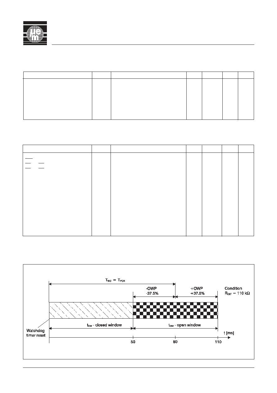
Watchdog Timeout Period Description
The watchdog timeout period is divided into two parts, a
"closed " window and an "open" window (see Fig. 3) and
is defined by two parameters, T
WD
and the Open Window
Percentage (OWP).
The closed window starts just after the watchdog timer re-
sets and is defined by T
CW
= T
WD
- OWP (T
WD
).
The open window starts after the closed time window fin-
ishes and lasts till T
WD
+ OWP (T
WD
). The open window
time is defined by T
OW
= 2 x OWP (T
WD
).
For example if T
WD
= 80 ms (actual value) and OWP = ±
37.5% this means the closed window lasts during first the
50 ms (T
CW
=50 ms = 80 ms - 0.375 (80 ms) ) and the
open window the next 60 ms (T
OW
= 2 x 0.375 (80 ms) =
60 ms). The watchdog can be serviced between 50 ms
and 110 ms after the timer reset. However as the time
base is ± 15% accurate.
Timer Clearing and RES Action
The watchdog circuit monitors the activity of the proces-
sor. If the users software does not send a pulse to the TCL
input within the programmed open window timeout pe-
riod a short watchdog RES pulse is generated which is
equal to T
WD
/32 = 2.5 ms typically (see Fig. 7).
With the open window constraint, new security is added
to conventional watchdogs by monitoring both software
cycle time and execution. Should software clear the
watchdog too quickly (incorrect cycle time) or too slowly
(incorrect execution), it will cause the system to be reset.
If the software is stuck in a loop which includes the rou-
tine to clear the watchdog, a conventional watchdog will
not reset the system even though the software is malfunc-
tioning; the V6175 will generate a system reset because
the watchdog is cleared too quickly. If no TCL pulse is ap-
plied before the closed and open windows expire, RES
will start to generate square waves of period - (T
CW
+
T
OW
+T
WDR
). The watchdog will remain in this state until
the next TCL falling edge appears during an open win-
dow, or until a fresh power-up sequence. The system en-
able output, EN, can be used to prevent critical control
functions being activated in the event of the system go-
ing into this failure mode (see section "Enable - EN Out-
put).
The RES output must be pulled up to V
DD
even if the out-
put is not used by the system (see Fig. 9 and 10).
Combined Voltage and Timer Action
The combination of voltage and timer actions is illustrated
by the sequence of events shown in Fig. 5. On power-up,
when the voltage at V
IN
reaches V
REF
, the power-on-reset,
POR, delay is initialized and holds RES active for the time
of the POR delay. A TCL pulse will have no effect until this
power-on-reset delay is completed. After the POR delay
has elapsed, RES goes inactive and the watchdog-timer
6
V6175
starts acting. If no TCL pulse occurs, RES goes active low
for a short time T
WDR
after each closed and open window
period. A TCL pulse coming during the open window
clears the watchdog timer. When the TCL pulse occurs
too early (during the closed window), RES goes active
and a new time-out sequence starts. A voltage drop be-
low the V
REF
level for longer than typically 5 µs, overrides
the timer and immediately forces RES active and EN inac-
tive. Any further TCL pulse has no effect until the next
power-up sequence has completed.
Enable - EN Output
The system enable output, EN, is inactive always when
RES is active and remains inactive after a RES pulse until
the watchdog is serviced correctly 3 consecutive times
(i.e. the TCL pulse must come in the open window). After
3 consecutive services of the watchdog with TCL during
the open window, the EN goes active low.
A malfunctioning system would be repeatedly reset by
the watchdog. In a conventional system critical motor
controls could be energized each time reset goes inac-
tive (time allowed for the system to restart) and in this way
the electrical motors driven by the system could function
out of control. The V6175 prevents the above failure
mode by using the EN output to disable the motor con-
trols until software has successfully cleared the watchdog
three times (i.e. the system has correctly restarted after a
reset condition).
Functional Description for Version 15
Mode's Conditions
Sleep
V
MAIN
> V
BAT
Mode
0
Yes
Main supply monitoring
0
No
Sleep
1
Yes
Watchdog
1
No
Battery monitoring
Table 7
Watchdog Mode
For the functionality of this mode see the paragraphs
"V
IN
Monitoring" and "Enable - EN Output".
Main Supply Monitoring
In this mode, the version 15 control the voltage at V
IN
in-
put. If V
IN
falls below V
REF
, the RES output goes active low.
When V
IN
becomes greater than V
REF
, the RES output is
held low for during the power-on reset (POR) delay.
Battery Monitoring Mode
In this mode, the version 15 works like in the Main Supply
Monitoring but the V
IN
input is switched to an internal ref-
erence of typically 2.85 V to control the battery level.
Sleep Mode
This is the very low power consumption mode, the RES
and EN output are in high state logic and TCL is inactive.
PFO Output
The version 15 has also a power-fail output which will be
active low when V
MAIN
is lower than V
BAT
.
7
V6175

8
V6175
Typical Applications
Version 05
Fig. 9
Version 15
Fig. 10

9
V6175
V
REF
versus V
DD
at T
A
= -40
o
C, +25
o
C, +85
o
C
Fig. 11
V
REF
versus Temperature at V
DD
= 3 V, 5 V
Fig. 13
V
REF
versus Temperature at V
DD
= 3 V and 5.5 V
V
REF
versus V
DD
at T
A
= -40
o
C, +25
o
C, +85
o
C
Fig. 12
Fig. 14

10
V6175
T
WD
versus Supply Voltage at T
A
< +85
o
C
Fig. 15
T
WD
versus Temperature at V
DD
= 5 V
Fig. 17
T
WD
versus R at V
DD
= 5 V
T
WD
versus V
DD
at T
A
< +125
o
C
Fig. 16
Fig. 18

11
V6175
T
WD
versus R at V
DD
= 5 V
Fig. 19

12
V6175
Package and Ordering Information
Dimensions of DIP14 Package
Dimensions in mm
Dimensions of SO14 Package
Fig. 21
Fig. 20
Dimensions in mm

13
V6175
Ordering Information
When ordering, please specify complete Part Number.
Part Number
Version
Package
Delivery Form
Package
Marking
(first line)
V6175V15SO14A
V15
14-pin SOIC
Stick
V6175 15S
V6175V15SO14B
V15
14-pin SOIC
Tape & Reel
V6175 15S
V6175V15TP16A
V15
16-pin TSSOP
Stick
V6175
V6175V15TP16B
V15
16-pin TSSOP
Tape & Reel
V6175
V6175V15DL14A
V15
14-pin plastic DIP
Stick
V6175 1514PI
For possible other versions please contact EM Microelectronic-Marin SA. Minimum order
quantity might apply.
Dimensions of TSSOP16 Package
Fig. 22
Dimensions in mm
EM Microelectronic-Marin SA cannot assume any responsibility for use of any circuitry described other than entirely
embodied in an EM Microelectronic-Marin SA product. EM Microelectronic-Marin SA reserves the right to change the
circuitry and specifications without notice at any time. You are strongly urged to ensure that the information given has
not been superseded by a more up-to-date version.
E. & O.E. Printed in Switzerland, Th
© 2002 EM Microelectronic-Marin SA, 03/02, Vers. B/455
EM Microelectronic-Marin SA, CH-2074 Marin, Switzerland, Tel. +41 - (0)32 75 55 111, Fax +41 - (0)32- 75 55 403