 | –≠–ª–µ–∫—Ç—Ä–æ–Ω–Ω—ã–π –∫–æ–º–ø–æ–Ω–µ–Ω—Ç: V6340P | –°–∫–∞—á–∞—Ç—å:  PDF PDF  ZIP ZIP |
Applications
Each applications needing a voltage detection :
n Computer electronics
White / Brown goods
Automotive electronics
Industrial electronics
Telecom systems
Hand-held systems
n
n
n
n
n
1
Features
n SOT-23 and TO-92 package
O
Reset output state guaranteed down to V = 1 V at 25 C
DD
Low supply current: stays stable during switching
versions B, N, N: typ. 19 µA at
±2.5% voltage threshold accuracy
High noise immunity
No external components required
Push-pull or Open drain output
Pin compatible with MAX 809 in SOT-23, by appropriate
layout on PCB
1)
Pin compatible with MC 33164 in TO-92 and SO8
TTL output compatibility
n
n
V = 5 V
DD
other Versions: typ. 38
m
A at V = 5 V,
DD
n
n
n
n
n
n
n
1)
On request
Description
The V6340 monitors the supply voltage of any electronic
system, and generates the appropriate Reset signal. The
threshold must be chosen to the minimum allowed voltage
which guarantees the good functionality of the system. As long
as V stays upside this voltage level, the output stays inactive.
If V drops below V , the output gets active. The threshold
DD
TH
voltage may be obtained in different versions: 2.6 V, 3.0 V, 3.7 V
and 4.4 V.
DD
Ultra Low Cost 3-Pin Microprocessor Reset
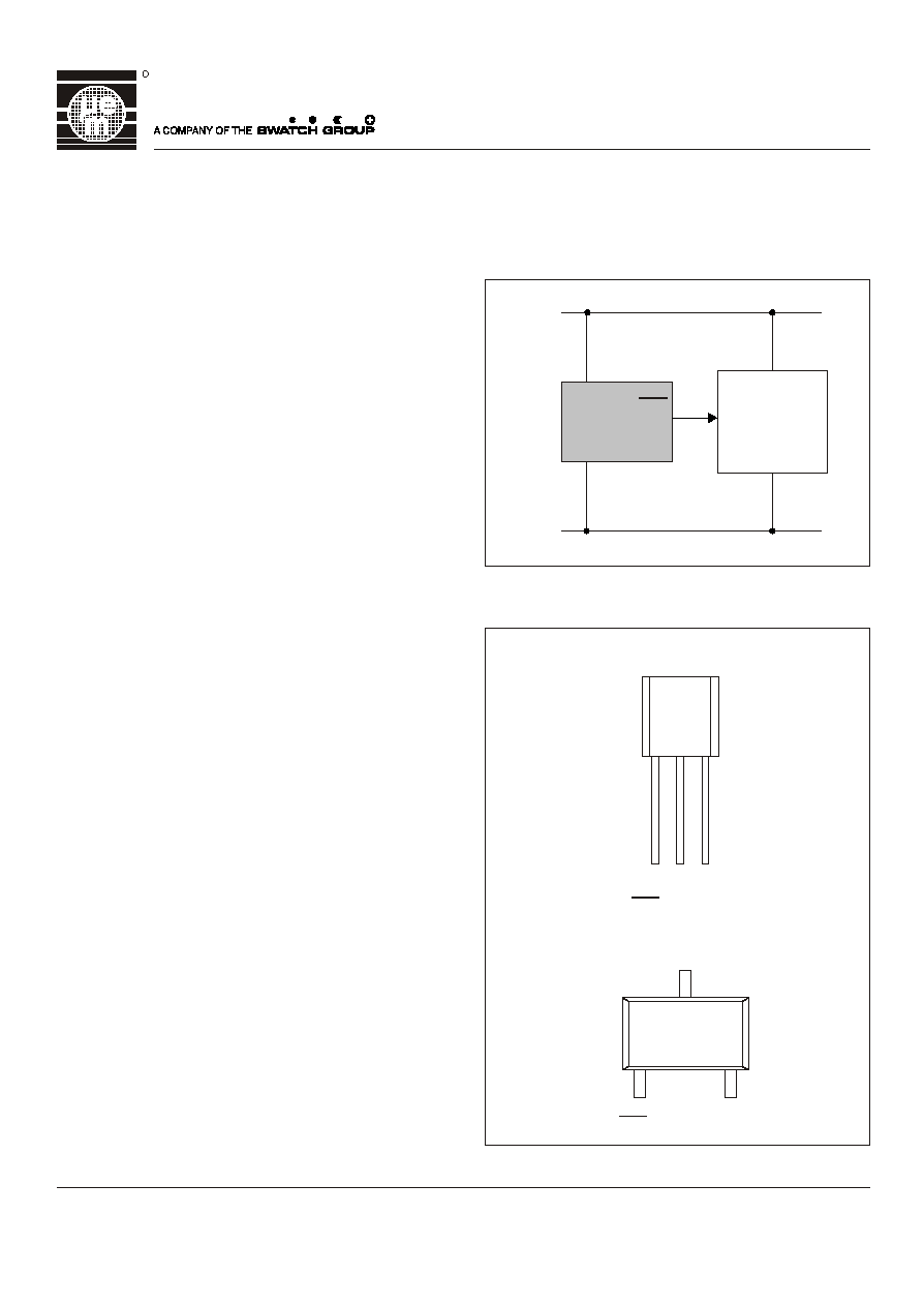
Pin Assignment
V
DD
V
DD
V
SS
1
1
2
2
3
3
V
SS
RES
or
RES
RES or
RES
V 6340
V 6340
View
Flat Front
TO-92
SOT-23
Fig. 2
Typical Operating Configuration
Fig. 1
V
DD
V
DD
V
SS
RES
or
RES
V 6340
GND
Micro-
processor
EM MICROELECTRONIC-MARIN SA
V6340
R

Handling Procedures
1)
The maximum operating temperature is confirmed by
sampling at initial device qualification. In production, all
devices are tested at +25
. On request devices tested at
+125
can be supplied.
2)
V = 1 V guaranteed at +2
(see Fig. 14 for more
DD
information)
O
C
O
C
O
5 C
2
Absolute Maximum Ratings
Stresses above these listed maximum ratings may cause
permanent damage to the device. Exposure beyond specified
operating conditions may affect device reliability or cause
malfunction.
Table 1
Parameter
Voltage at V
to V
DD
SS
Min. voltage at RES or RES
Mix. voltage at RES or RES
Storage temperature range
V
DD
V
min
V
max
T
STO
-0.3V to+8V
V
- 0.3V
SS
-65 to + 150
O O
C
V
+ 0.3V
DD
Symbol
Conditions
Electrical Characteristics
O
T = +25 C, unless otherwise specified
A
1)
Only for Open drain versions
I
DD
V
TH
V = 5 V, output open
DD
B,H,N
2.56
19
31
2.74
2.65
Supply current
Threshold voltage
Threshold hyteresis V
32 mV
HYS
m
A
V
Table 3
Only for version B, H and N
I
DD
V
TH
V
TH
V
TH
V
HYS
V
OL
V
OL
V
OL
V
OL
V
OH
V
OH
V
OH
V
OH
I
LEAK
V = 5 V, output open
DD
C, I, O
2.94
38
50
3.10
3.82
4.51
270
250
250
250
1
3.02
3.72
4.39
5
200
195
198
185
1.36
2.3
3.27
4.76
0.005
1.25
2.2
3.15
4.65
D, J, P
3.62
F, L, R
4.27
V = 1.6 V, I = 1mA
DD
OL
V = 2.5 V, I = 2mA
DD
OL
V = 3.5 V, I = 3mA
DD
OL
V = 5 V, I = 4mA
DD
OL
V = 1.6 V, I = -1mA
DD
OH
V = 2.5 V, I = -1.5 mA
DD
OH
V = 3.5 V, I = -2.5mA
DD
OH
V = 5 V, I = -3.5 mA
DD
OH
V = 5 V
DD
Supply current
Threshold voltage
Threshold hysteresis
RES Output Low Level
RES Output High Level
1)
Output leakage current
m
A
V
V
V
mV
mV
mV
mV
mV
V
V
V
V
m
A
Parameter
Symbol
Test Conditions
Min.
Typ.
Max.
Units
This device has built-in protection against high static voltages
or electric fields; however, anti-static precautions must be taken
as for any other CMOS component. Unless otherwise specified,
proper operation can only occur when all terminal voltages are
kept within the supply voltage range.
Operating Conditions
T
A
-40
1
+125
O
C
V
5.5
V
DD
Table 2
Parameter
Symbol Min. Typ . Max. Units
1)
Operating temperature
2)
Positive supply voltage
Timing Waveform
Block Diagram
Fig. 4
V
DD
V
SS
Voltage
Reference
RES or RES
-
+
V
TH
1 V
Logic "1"
Logic "0"
Logic "1"
Logic "0"
RES
Fig. 3
t
t
t
RES
V
DD
V6340
R
3
[1]* Multiply value at +25
by this factor to determine the
value at temperature
O
C
V - V vs. Supply Voltage
DD
OH
V
-
V
[
m
V
]
D
D
O
H
V
[V]
DD
Fig. 9
500
400
300
200
100
0
1.5
2
2.5
3
3.5
4
4.5 5
I
= 4mA
OH
I
= 2mA
OH
I
= 1mA
OH
I
= 500
m
A
OH
V vs. Supply Voltage
OL
V
[
m
V
]
O
L
V
[V]
DD
500
400
300
200
100
0
1.5
2.5
3.5
4.5
Fig. 8
I
= 4mA
OL
I
= 2mA
OL
I
= 1mA
OL
I
= 500
m
A
OL
Typical Characteristics
Normalized V vs. Temperature
OL
Normalized V vs. Temperature
OH
V
[
1
]
*
O
H
1.06
1.04
1.02
1
0.98
0.96
0.94
-50
0
+50
0
T [ C]
A
+100
Fig. 5
V =1.6V, I
=1mA
DD
OH
V =2.5V, I
=1.5 mA
DD
OH
V =3.5V, I
=2.5 mA
DD
OH
V =5V, I
=3.5 mA
DD
OH
V vs. Output Current
OL
V - V vs. Output Current
DD
OH
V
-
V
[
m
V
]
D
D
O
H
I [mA]
OH
800
700
600
500
400
300
200
100
0
0
2
4
6
8
Fig. 7
V =1.6 V
DD
V =2.5 V
DD
V =5 V
DD
V =3.5 V
DD
V
[
m
V
]
O
L
I [mA]
OL
500
400
300
200
100
0
2
4
6
8
0
Fig. 6
V =1.6 V
DD
V =2.5 V
DD
V =5 V
DD
V =3.5 V
DD
1.6
1.4
1.2
1
0.8
0.6
-50
0
+50
T [
]
A
O
C
+100
Fig. 4
V
[
1
]
*
O
L
V6340
R

4
Supply Current vs. Temperature
Normalized Threshold vs. Temperature
70
60
50
40
30
20
10
0
I
[
m
A
]
D
D
I
[
m
A
]
D
D
-50
+50
+100
0
o
T [ C]
A
o
T [ C]
A
Fig. 10
V
= 5V
DD
V
= 4V
DD
V
= 3V
DD
V
= 2V
DD
V
= 1.6V
DD
1.02
1.015
1.01
1.005
1
0.995
0.99
0.985
0.98
T
h
r
e
s
h
o
l
d
[
1
]
*
-50
-50 -25 0 +25 +50 +75 +100 +125
+50
+100
0
o
T [ C]
A
Fig. 11
Typical Sensivity vs. Temperature
Typical Sensivity vs. Temperature
Typical Minimum Operating Supply Voltage (V
)
DD
O
[1]* Multiply value at +25
C
by this factor to determine the value at temperature
1.6
1.4
1.2
1
0.8
0.6
0.4
0.2
0
S
u
p
p
l
y
V
o
l
t
a
g
e
[
V
]
O
T [
C
]
A
Fig. 14
V6340
R
35
30
25
20
15
10
5
-50 -25
0
+25
+50 +75 +100 +125
T
[
m
S
]
S
E
N
o
T [ C]
A
Fig. 12
Output inactive
400 mV
T
SEN
T
SEN
V
TH
V
DD
Output active
Version C, I, O
Version
D, J, P
Version F, L, R
o
T [ C]
A
Fig. 13
740
700
660
620
580
540
500
-50
-25
0
+25
+50 +75 +100 +125
T
[
m
S
]
S
E
N
Output inactive
5V
2V
Output active
All Versions
T
SEN
T
SEN
V
TH
V
DD
-40 -20 0 +20 +40 +60 +80 +100 +120
35
30
25
20
5
10
5
0
Only for versions B, H, N
V
= 5V
DD

5
Solar Cell Power O.K. Indicator
Fig. 17
-
+
Voltage
Reference
Load
V
SS
V
DD
820
W
RES
HLMP-1700
Accurate High Voltage Monitoring
Use only a push-pull version
Fig. 18
Voltage
Reference
Output
+
+
V = R (
T
1
I
+
DD
R
2
V
TH
+ V
TH
)
V
CC
V
IN
R
1
R
2
In1
Out1
V
SS
V
DD
OE
Typical Applications
Reset Circuit with Hysteresis
Voltage Monitor with Manual Reset
-
+
Voltage
Reference
V
SS
Output
V
DD
V
DD
Use only an active low version
V = V + R - I
T
TH
1
DD
R
1
Fig. 15
-
+
Voltage
Reference
V
SS
Output
22nF
V
DD
V
DD
Use only an active low version
V = V + R - I
T-
TH
1
DD
R
1
Fig. 16
V = V + R
T+
TH
1
I
DD
R
2
V - V
TH
OL
R
2
V6340
R