
Rev 0.95 ≠ March 2005 www.enpirion.com
1
ENPIRION
EN5310
1A Voltage Mode Synchronous Buck PWM
DC-DC Converter
Description
The EN5310 is a Power System on a Chip DC-DC
converter. It is specifically designed to meet the
precise voltage and fast transient requirements of
present and future high-performance, low-power
processor, DSP, FPGA, memory boards and system
level applications in a distributed power architecture.
Advanced circuit techniques, ultra high switching
frequency, and very advanced, high-density,
integrated circuit and proprietary inductor technology
deliver high-quality, ultra compact, non-isolated DC-
DC conversion. Operating this converter requires only
three external components that include small value
input and output ceramic capacitors and a soft-start
capacitor.
The EN5310 significantly helps in system design and
productivity by offering greatly simplified board
design, layout and manufacturing requirements. In
addition, a reduction in the number of vendors
required for the complete power solution helps to
enable an overall system cost savings.
Typical Application Circuit
VID Output
Voltage Select
V
OUT
V
IN
VSENSE
22µ
F
10µ
F
15nF
VOUT
VS0
VS1
VS2
POK
PGND
AGND
SS
PVIN
AVIN
Features
∑ 1000mA output current capacity
∑ External inductor is NOT required
∑ Lead-Free packaging
∑ 5MHz operating frequency
∑ More than 90% efficient
∑ V
OUT
accuracy of 2% over line, load and
temperature
∑ 1/2 the board area of discrete component solutions
∑ Very fast transient response
∑ All high speed switching signals contained inside
the part
∑ Wide input voltage range of 2.375V to 5.5V
∑ Digital voltage selector with options for common
output voltages from 0.8V to 3.3V
∑ External resistor divider and OVP option for
programming output voltages from 0.9V to 4.0V
∑ Output enable pin and Power OK signal
∑ Programmable soft-start time
∑ Programmable over-current protection
∑ Thermal shutdown, short circuit, over-voltage and
under-voltage protection
Applications
∑ VOIP phones, video telephones
∑ Broadband, networking, LAN/WAN, optical
telecommunications equipment
∑ Point of load regulation for low-power processors,
network processors, DSPs, FPGAs, and ASICs
∑ Low voltage, distributed power architectures with
2.5V, 3.3V or 5V rails
Ordering Information
Part Number
Temp Rating (∞C)
Package
EN5310DC
0 to 70
36-pin DFN
EN5310DC-T
0 to 70
36-pin DFN T&R
EN5310DI
-40 to +85
36-pin DFN
EN5310DI-T
-40 to +85
36-pin DFN T&R
EN5310DC-E
DFN Evaluation Board

Rev 0.95 ≠ March 2005
www.enpirion.com
EN5310
2
Pin Configuration
This diagram is a top-view of the component and represents the on-board layout requirements for the
landing pads and thermal connection points. Specific dimensions for the pads are presented on page 10.
Pin 1 of the device is signified by the white dot marked on the top of the device.
Block Diagram
Rev 0.95 ≠ March 2005
www.enpirion.com
EN5310
3
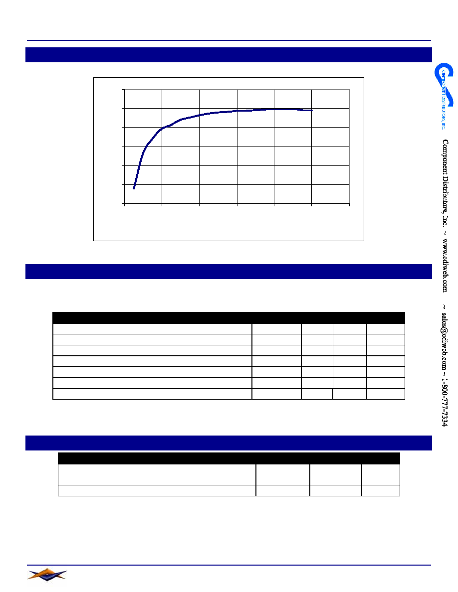
Typical Efficiency
V
IN
= 3.3V and V
OUT
= 2.5V
40%
50%
60%
70%
80%
90%
100%
0
200
400
600
800
1000
1200
Output Current (mA)
Absolute Maximum Ratings
CAUTION: Stresses in excess of the absolute maximum ratings can cause permanent damage to the device.
Exposure to absolute maximum ratings for extended periods can adversely affect device reliability.
PARAMETER
SYMBOL MIN
MAX UNITS
Input Supply Voltage
V
IN
-0.5 6.5 V
Input Voltage ≠ Enable
-0.5
V
IN
V
Input Voltage ≠ VS0, VS1 & VS2 (Note 1)
-0.5
2.8
V
Storage Temperature Range
T
STG
-65 150 ∞C
Operating Junction Temperature
T
J
150 ∞C
MSL per JEDEC J-STD-020A Level 3 (Note 2)
240
∞C
ESD Rating (based on Human Body Model)
2000
V
NOTES:
1. VS0, VS1 and VS2 pins have an internal pull-up resistor, only ground potentials should be placed on them as required.
2. Evaluation for MSL3 at 255∞C in process.
Thermal Characteristics
PARAMETER
SYMBOL
TYPICAL UNITS
Thermal Resistance: Junction to Ambient (0 LFM)
(Note 3)
JA
36 ∞C/W
Thermal Resistance: Junction to Case (0 LFM)
JC
6 ∞C/W
NOTES:
3. Based on a four-layer board and proper thermal design.

Rev 0.95 ≠ March 2005
www.enpirion.com
EN5310
4
Electrical Characteristics
NOTE: V
IN
=3.3V and over operating temperature range unless otherwise noted. Typical values are at T
A
=
25∞C.
PARAMETER
SYMBOL
TEST CONDITIONS
MIN
TYP
MAX UNITS
Operating Input
Voltage
V
IN
2.375
5.5
V
Quiescent Supply
Current
I
Q
No switching, AVIN = 3.3V,
PVIN = 3.3V, ENABLE=0V
15 mA
No-Load Operating
Current
I
NL
Includes PWM, gate drive and
inductor ripple current.
35 mA
Switching
Frequency
F
OSC
5
MHz
Thermal Overload
Trip Point
T
J
160 ∞C
V
OUT
Range V
OUT
Using external voltage divider
0.9
V
Accuracy V
OUT
Over line, load and temperature
2.0
%
Line Regulation
V
OUT
V
IN
= 2.5 to 5.0 volts
3
mV
Load Regulation
V
OUT
I
LOAD
= 0 to 1A
3
mV
V
OUT
T
A
= 0 to 70∫C
TBD
mV
Temperature
Regulation
V
OUT
T
A
= -40 to 85∫C
TBD
mV
Transient Response (I
OUT
= 0% to 100% or 100% to 0% of Rated Load)
Peak Deviation
V
OUT
V
IN
= 5V, 1.2V < V
OUT
< 3.3V
2
5
%
Output Voltage Ripple
Peak-to-peak V
OUT-PP
V
IN
= 5.0V, V
OUT
= 1.2V, I
OUT
= 1A,
C
OUT
= 20uF, 2 x 10µF X5R or X7R
ceramic capacitors
12 mV
Maximum Continuous Output Current (Note 4)
Output Current
I
OUT
1000
mA
Enable Operation
Disable Threshold
V
DISABLE
Max voltage to ensure the converter
is disabled
0.8
V
Enable Threshold
V
ENABLE
Min voltage to ensure the converter
is enabled
1.8 V
Power OK Operation
POK low voltage
V
POK
I
POK
= 1mA
0.4
V
Max POK Voltage
V
POK
Supply voltage applied to POK
5.5
V
NOTES:
4. Maximum output current may need to be de-rated, based on operating condition, to meet T
J
requirements.

Rev 0.95 ≠ March 2005
www.enpirion.com
EN5310
5
Pin Descriptions
PIN
NAME
FUNCTION
1
NC
NO CONNECT ≠ Do not electrically connect this pin to PCB. See Note 5.
2 XFB
External feedback voltage input. Option for programming the output voltage with a
resistor divider on V
OUT
.
3 VSENSE
Remote voltage sense input. Connect this pin to the load voltage at the point to be
regulated.
4
NC
NO CONNECT ≠ Do not electrically connect this pin to PCB. See Note 5.
5
NC
NO CONNECT ≠ Do not electrically connect this pin to PCB. See Note 5.
6
ENABLE
Enable input. An input high enables operation. An input low disables operation.
7
NC
NO CONNECT ≠ Do not electrically connect this pin to PCB. See Note 5.
8 XOV
Over-Voltage set-point input. When using an external voltage divider and the XFB pin. When
VS0, VS1 and VS2 are left OPEN or pulled high, an additional voltage divider separate from
the XFB pin is required to set the OVP set-point. In this mode, the OVP function is disabled if
this voltage divider is not present.
9
10
11
12
PGND
Power ground for the power stage circuits.
13
14
15
16
17
18
VOUT
Voltage and power output.
19
NC
NO CONNECT ≠ Do not electrically connect this pin to PCB. See Note 5.
20
21
22
23
PGND
Power ground for the power stage circuits.
24
NC
NO CONNECT ≠ Do not electrically connect this pin to PCB. See Note 5.
25
26
27
28
PVIN
Power voltage input for the power stage circuits.
29
VS2
Voltage select line 2 input. See Table 1.
30
ROCP
Over-Current trip point adjust input. Used for adjusting the OCP trip point.
31
VS1
Voltage select line 1 input. See Table 1.
32
AVIN
Analog voltage input for the controller circuits.
33
AGND
Analog ground for the controller circuits.
34
VS0
Voltage select line 0 input. See Table 1.
35
POK
Power OK is an open drain transistor for power system state indication.
36
SS
Soft-Start node. A capacitor is connected between this pin and AGND.
NOTES:
5. This pin is used for engineering test purposes and reserved for future use. Solder, but do not electrically connect this pin to
the PCB.