4800 Great America Parkway, Suite 202
Tel: 408-235-8680
Santa
Clara,
CA
95054
Fax:
408-235-8685
1
EN29F040
Rev. D, Issue Date: 2001/07/05
FEATURES
∑
5.0V operation for read/write/erase
operations
∑
Fast Read Access Time
- 45ns, 55ns, 70ns, and 90ns
∑
Sector Architecture:
- 8 uniform sectors of 64Kbytes each
- Supports full chip erase
- Individual sector erase supported
- Sector protection:
Hardware locking of sectors to prevent
program or erase operations within
individual sectors
∑
High performance program/erase speed
- Byte program time: 10µs typical
- Sector erase time: 500ms typical
- Chip erase time: 3.5s typical
∑
Low Standby Current
- 1µA CMOS standby current-typical
- 1mA TTL standby current
∑
Low Power Active Current
- 30mA active read current
- 30mA program/erase current
∑
JEDEC Standard program and erase
commands
∑
JEDEC standard DATA polling and toggle
bits feature
∑
Single Sector and Chip Erase
∑
Sector Unprotect Mode
∑
Embedded Erase and Program Algorithms
∑
Erase Suspend / Resume modes:
Read and program another Sector during
Erase Suspend Mode
∑
0.35 µm double-metal double-poly
triple-well CMOS Flash Technology
∑
Low Vcc write inhibit < 3.2V
∑
100K endurance cycle
∑
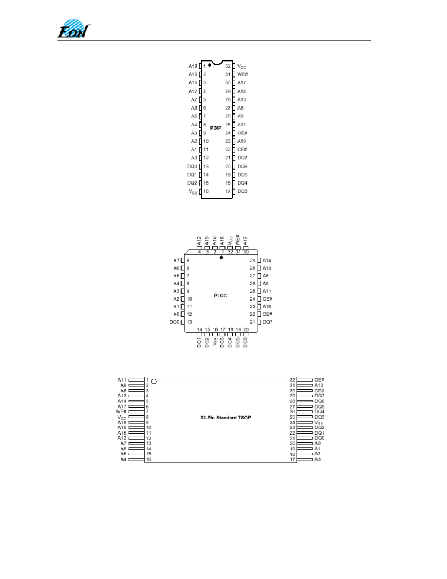
Package Options
- 32-pin PDIP
- 32-pin PLCC
- 32-pin TSOP (Type 1)
∑
Commercial and Industrial Temperature
Ranges
GENERAL DESCRIPTION
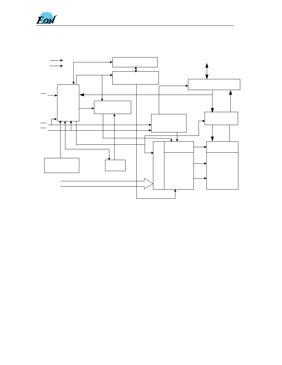
The EN29F040 is a 4-Megabit, electrically erasable, read/write non-volatile flash memory. Organized
into 512K words with 8 bits per word, the 4M of memory is arranged in eight uniform sectors of
64Kbytes each. Any byte can be programmed typically in 10µs. The EN29F040 features 5.0V
voltage read and write operation, with access times as fast as 45ns to eliminate the need for WAIT
states in high-performance microprocessor systems.
The EN29F040 has separate Output Enable ( OE ), Chip Enable (
CE
), and Write Enable (
W E
)
controls, which eliminate bus contention issues. This device is designed to allow either single
(or
multiple) Sector or full chip erase operation, where each Sector can be individually protected against
program/erase operations or temporarily unprotected to erase or program. The device can sustain a
minimum of 100K program/erase cycles on each Sector.
EN29F040
4 Megabit (512K x 8-bit) Flash Memory
4800 Great America Parkway, Suite 202
Tel: 408-235-8680
Santa
Clara,
CA
95054
Fax:
408-235-8685
5
EN29F040
Rev. D, Issue Date: 2001/07/05
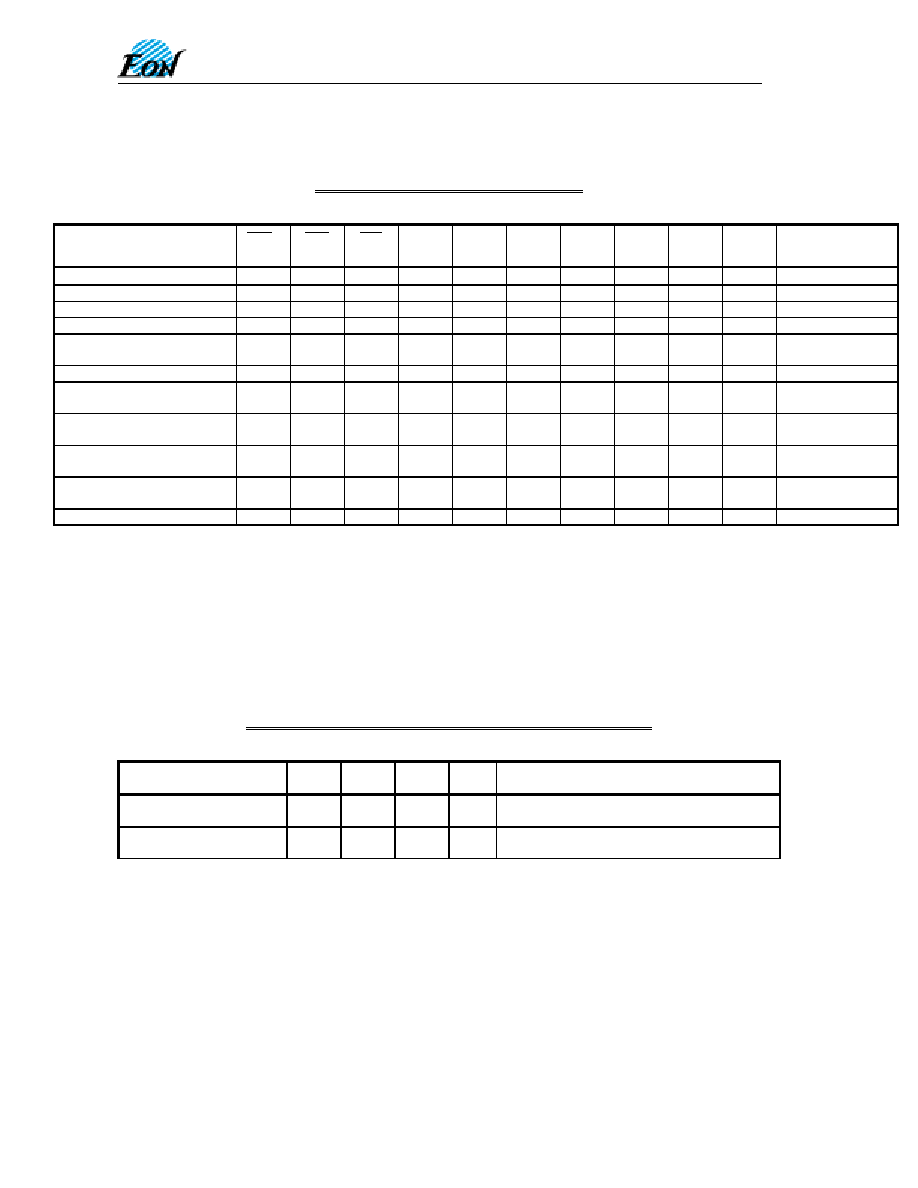
TABLE 3. OPERATING MODES
4M FLASH USER MODE TABLE
C E
WE
OE
A9 A8 A6 A5 A1 A0 Ax/y DQ(0-7)
USER MODE
STANDBY
H X X X X X X X X X
HI-Z
READ
L H L A9 A8 A6 A5 A1 A0 Ax/y DQ
(0-7)
OUTPUT
DISABLE L H H X X X X X X X
HI-Z
READ
MANUFACTURE ID
L H L
VID
L/H L X L L X
MANUFACTURE
ID
READ DEVICE ID
L
H
L
VID
L/H
L
X
L
H
X
DEVICE ID (T/B)
VERIFY SECTOR
PROTECTION
L H L
VID
X L X H L X
CODE
SECTOR
PROTECTION
L Pulse
L
VID
VID
X L X X X X
X
VERIFY SECTOR
UNPROTECTION
L H L
VID
X H X H L X
CODE
SECTOR
UNPROTECTION
Pulse
L
VID
VID
L X X H X X X
X
WRITE
L L H A9 A8 A6 A5 A1 A0 Ax/y DIN
(0-7)
NOTES:
1) L
=
V
IL
, H = V
IH
, V
ID
= 11.0V
±
0.5V
2) X = Don't care, either V
IH
or V
IL
3) Ax/y: Ax = Addr(x), Ay = Addr(y)
TABLE 4. DEVICE IDENTIFICTION
4M FLASH MANUFACTURER/DEVICE ID TABLE
A8 A6 A1 A0
DQ(7-0)
HEX
READ
MANUFACTURER ID
H
(1)
L L L
MANUFACTURER ID
1C
READ
DEVICE ID
H
(2)
L L H
DEVICE ID
04
NOTES:
1) If a Manufacturing ID is read with A8 = L, the chip will output a configuration code 7Fh. A further
Manufacturing ID must be read with A8 = H.
2) If a Device ID is read with A8 = L, the chip will output a configuration code 7Fh. A further Device ID
must be read with A8 = H.