
EG-2102CA Rev 1.1 2Y5
EG-2102CA
-High frequency PECL Oscillator-
Features
∑
Generates high frequency clock from a high stability SAW (surface acoustic wave) resonator.
∑
Differential LV-PECL output.
∑
Very low jitter/low phase noise.
∑
Small SMD in 7x5mm, Max1.4mm height, ceramic package.
Applications
∑
10Gigabit Ethernet, Fibre channel, High-end Server
Absolute Maximum Ratings
Item Symbol
Unit
MIN.
TYP.
MAX. Condition
Supply Voltage
V
CC
V -0.5 +4.0
V
CC
- GND
Storage temperature
Tstg
∞
C
-40
+100
Stored as bare product after
unpacking
Solder heat resistance of the
outer lead
Tsol
Max. 240
∞
C x Max. 10s x 2 times
Operating range
Item Symbol
Unit
MIN.
TYP.
MAX. Condition
Supply voltage
V
CC
V 3.0 3.3 3.6
0 +70
P
version
Operating temperature
T
OPR
∞
C
-5 +85
R
version
Output load
RL
50
Terminated to V
CC
-2V
Frequency characteristics (V
CC
=3.0 to 3.6,GND=0.0V,Load=Max,Output bias=Vcc-2.0V)
Item Symbol
Unit
MIN.
TYP.
MAX. Condition
Oscillation Range
fosc
MHz
100
700
+/-100
H stability *1
Frequency Stability
df/f0
ppm
+/-50
G stability *1
Aging
dfa
ppm
+/-5 1
st
year
N (Excluding Aging) condition
*1 This includes initial frequency tolerance, temperature variation, supply voltage variation, load variation and reflow drift.
Condition "A" includes 10yrs aging. Condition "N" doesn't include aging.
Electrical characteristics (V
CC
=3.0 to 3.6,GND=0.0V,Load=Max,Output bias=Vcc-2.0V)
Item Symbol
Unit
MIN.
TYP
MAX. Condition
Start up time
t
osc
ms
10
t=0 at V
CC
=3.135V
Current consumption
I
OP
mA 80 100
With 50
load
Disable current
I
OE
mA
32
OE=GND
Rise time
t
TLH
ps
400
20-80% of (VOH-VOL)
Fall time
t
THL
ps
400
80-20% of (VOH-VOL)
45
55
P version. 100 to 700MHz
Duty
at outputs crossing point
tw/t %
48 52
D
version.
<350MHz
High level output voltage
V
OH
V
Vcc-1.03
2.35
Vcc-0.88
V
CC
=3.3V, *4
Low level output voltage
V
OL
V
Vcc-1.81
1.60
Vcc-1.62
V
CC
=3.3V
High level input voltage
V
IH
V 0.7V
CC
OE Terminal.
Low level input voltage
V
IL
V
0.3V
CC
OE Terminal.
Output disable time
T
PXZ
ns
100
When OE turns High to Low.
Output enable time
T
PZX
ns
100
When OE turns Low to High.
UI
0.072x10
-3
12KHz to 20MHz, rms
Phase Jitter *2
t
PJ
UI
0.103x10
-3
50KHz to 80MHz, rms
t
DJ
ps
5 10
Deterministic
Jitter
t
RJ
ps
3
4
of Random Jitter
t
RMS
ps
3
4
of Total jitter distribution
Period Jitter *3
n=50000 samples
t
p-p
ps
25
40
Peak to Peak of jitter distribution
Accumulated Jitter *3
n=2 to 50000 cycles
t
acc
ps
4
5
of Total jitter distribution
*2 Measured by SSB phase noise test equipment. *3 Measured by Time interval analyzer or oscilloscope. *4 V
OH
= Vcc-1.09 MIN at Ta<0
∞
C
EPSON ELECTRONICS AMERICA, INC.
www.eea.epson.com
EG-2102CA Rev 1.1 2Y5
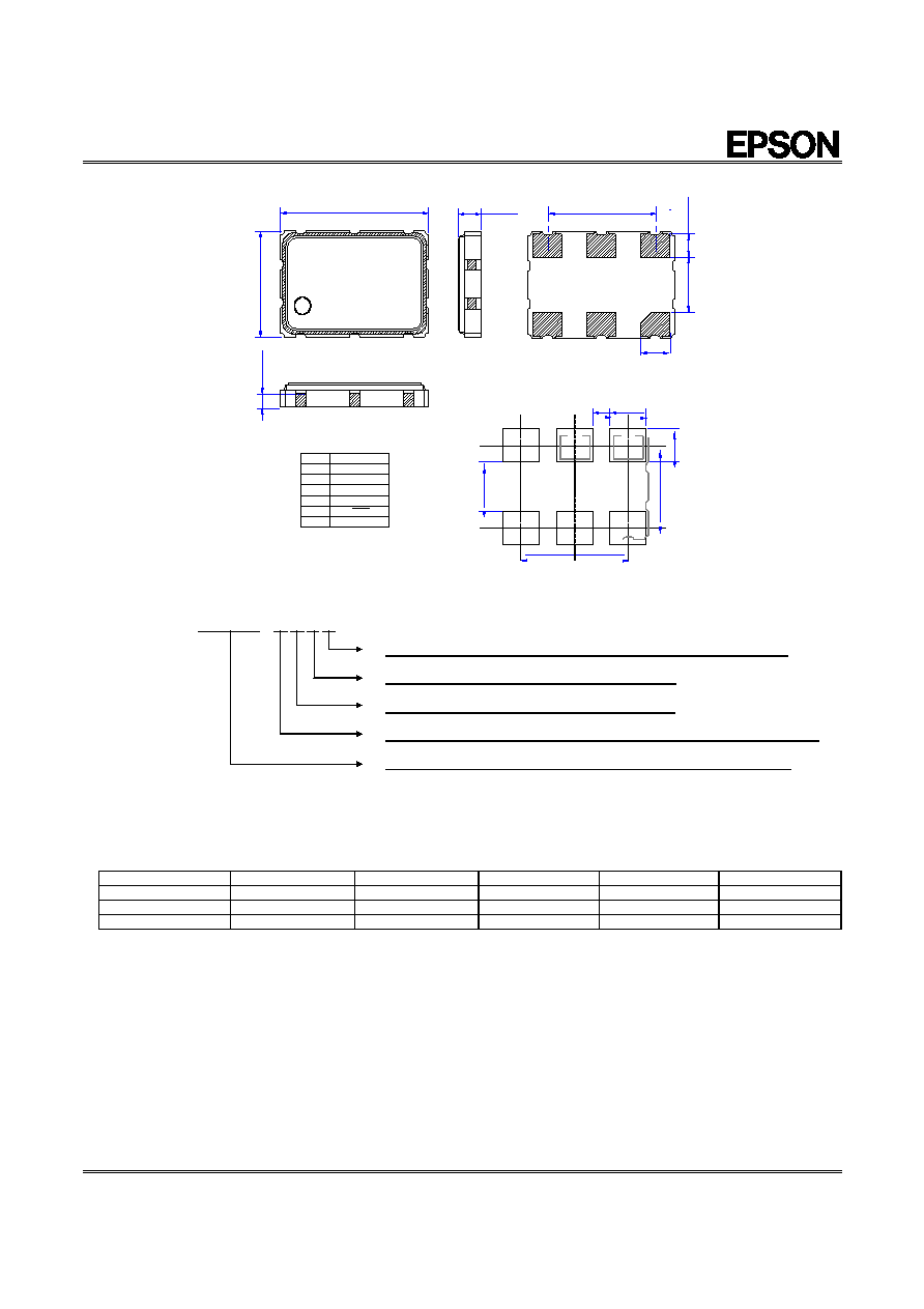
External Dimensions ( Unit : mm )
1.40
E EG-2102
644.531P
HPA21MA
7.0
±
0.2
5.08
1.4 Max
5.
0
±
0.
2
0.
70
2.
60
1.
10
#3
#2
#1
#1
#4 #5
#5
#6
#6
#4
#2
#3
No.
#1
#2
#3
#4
Pin
Name
OE
N.C.
GND
OUT
#5
#6
OUT
V
CC
∑
Soldering pattern
(
M
e
t
a
lliz
e
)
1.60
0.94
5.08
1.
5
0
3.
9
0
2.
40
Part Numbering Guide *1
EG-2102CA - (Frequency)M - P H P A
Stability condition A: Including 10yrs Aging N: Excluding Aging
Temperature Range P: 0 to +70C R: - 5 to +85C
Frequency Stability H: +/-100ppm G: +/-50ppm
Output P: LVPECL (Duty +/-5%) D: LVPECL (Duty +/-2%) *2
Output Frequency : see Standard frequency list (4-Digit accuracy)
*1: Available combination :
xHPA, xHPN, xHRA, xHRN, xGPN
For
xGPA and xGRN, please contact Epson.
xGRA is not available.
*2: D (Duty+/-2%) is available under 350MHz.
Standard Frequency List
100.0000
106.2500
125.0000
155.5200
156.2500
161.1328 *3
200.0000
212.5000
250.0000
311.0400
312.5000
322.2656 *4
400.0000
425.0000
500.0000
622.0800
625.0000
644.5313 *5
159.3750
Please round off 5
th
digit specify 4-digit accuracy under decimal point.
Nominal frequency: *3=161.1328125MHz, *4=322.265625MHz, *5=644.53125MHz
EPSON ELECTRONICS AMERICA, INC.
www.eea.epson.com
