1
DATA SHEET
EPSON ELECTRONICS AMERICA, INC.
i
150 River Oaks Pkwy
i
San Jose, CA 95134
i
Tel: (408) 922-0200
i
Fax: (408) 922-0238
ASIC
S1L50000
S1L50000 SERIES HIGH DENSITY GATE ARRAY
DESCRIPTION
EPSON Electronics America, Inc.'s
S1L50000 Series is a family of ultra high-speed VLSI CMOS
gate array utilizing a 0.35
µ
m "sea-of-gates" architecture. The
S1L50000H products feature 5V
tolerant I/O buffers.
∑
Ultra-high-speed, high density and low power consumption
∑
Low voltage operation: 3.3V and 2.0V
∑
Number of raw gates: 28,710 ~ 815,468 gates
FEATURES
∑
Process
0.35
µ
m 2/3/4 layer metalization CMOS process
∑
Integration
A maximum of 815,468 gates (2 input NAND gate equivalent)
∑
Operating Speed
Internal gates: 140 ps (3.3V Typ), 210 ps (2.0V Typ)
(2-input pair NAND, F/O = 2, Typical wire load)
Input buffer:
380 ps (5.0V Typ) Built-in level shifter is used.
400 ps (3.3V Typ), 1.30 ns (2.0V Typ)
(F/O = 2, Typical wire load)
Output buffer: 2.12 ns (5.0V Typ) Built-in level shifter is used.
2.02 ns (3.3 V Typ), 3.90 ns (2.0V Typ)
(C
L
= 15 pF)
∑
I/F Levels
Input/Output TTL/CMOS/LVTTL compatible
∑
Input Modes
TTL, CMOS, LVTTL, TTL Schmitt, CMOS Schmitt, LVTTL Schmitt, PCI
Built-in pull-up and pull-down resistors can be usable.
(2 types for each resistor value)
∑
Output Modes
Normal, 3-state, bi-directional, PCI
∑
Output Drive
I
OL
= 0.1, 1, 3, 8, 12, 24 mA selectable
(Built-in level shifter is used at 5.0V)
I
OL
= 0.1, 1, 2, 6, 12 mA selectable (at 3.3V)
I
OL
= 0.05, 0.3, 0.6, 2, 4 mA selectable (at 2.0V)
∑
RAM
Asynchronous 1-port, asynchronous 2-port
∑
Dual Power
Operation supported by using level-shifter circuit
Internal logic: Operation supported by low voltage
I/O Buffer:
Built-in interfaces of both high and low voltages possible
∑
Operation possible at V
DD
= 2.0
±
0.2V
2
EPSON ELECTRONICS AMERICA, INC.
i
150 River Oaks Pkwy
i
San Jose, CA 95134
i
Tel: (408) 922-0200
i
Fax: (408) 922-0238
ASIC
S1L50000
DATA SHEET
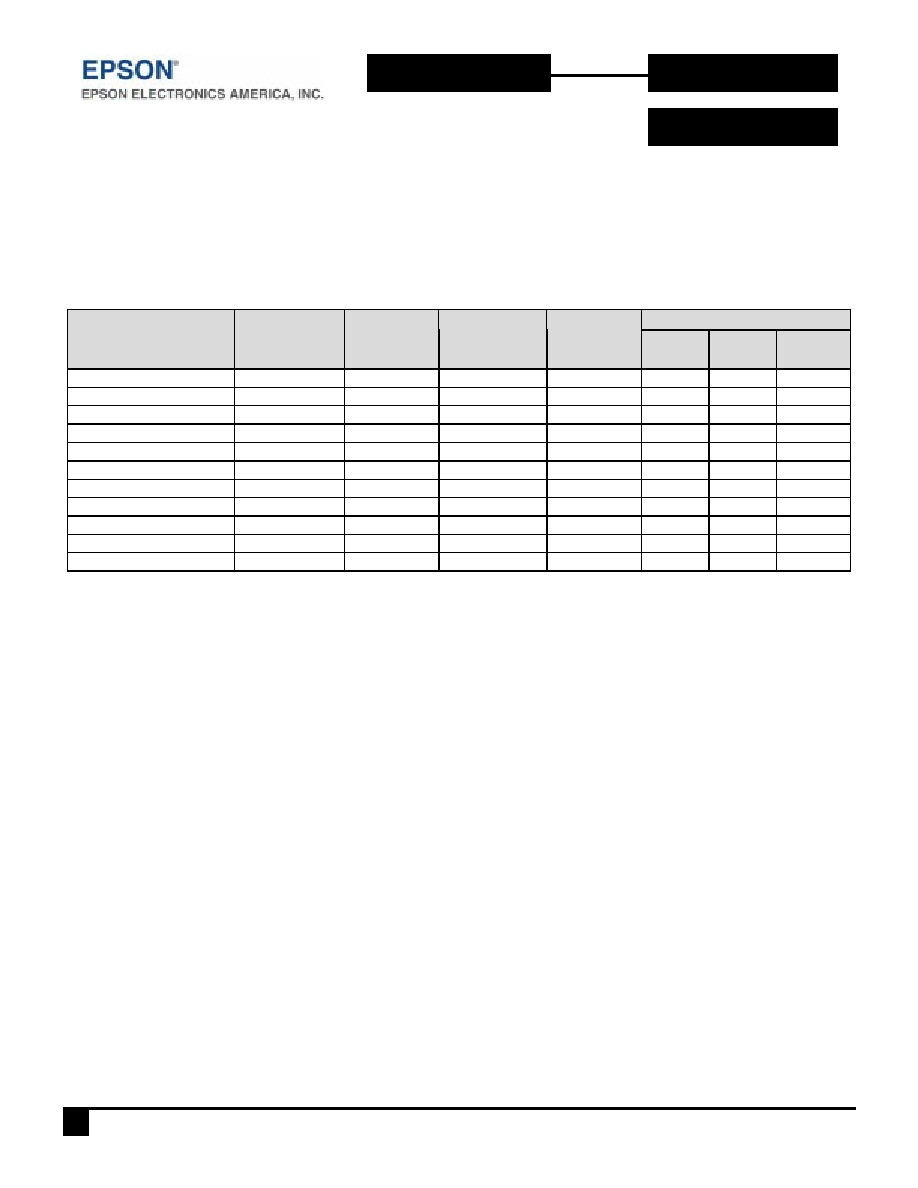
LINE UP
The
S1L50000 Series comprises 11 types of masters, from which the customer is able to select
the master most suitable.
Cell Utilization Ratio (U)
*1
Master
Total
BC
(Raw Gates)
Number
of
Pads
Number
of
Columns (X)
Number
of
Rows (Y)
2-layer
metal
3-layer
metal
4-layer
metal
S1L50282/283/284 28710
88
319
90
50%
88%
95%
S1L50752/753/754 75774
144
519
146
47%
85%
95%
S1L50992/993/994 99198
168
594
167
47%
85%
95%
S1L51252/253/254 125772
188
669
188
45%
80%
95%
S1L51772/773/774 177062
224
794
223
45%
75%
95%
S1L52502/503/504 250160
264
944
265
45%
75%
95%
S1L53352/353/354 335858
308
1094
307
43%
75%
95%
S1L54422/423/424 442112
352
1256
352
40%
70%
90%
S1L55062/063/064 506688
376
1344
377
40%
70%
90%
S1L56682/683/684 668552
432
1544
433
40%
70%
90%
S1L58152/153/154 815468
480
1706
478
40%
70%
90%
NOTE:
*
1: This is the value when there are no cells, such as RAM cells. The cell use efficiency is dependent not only on the scope of
the circuits, but also on the number of signals, the number of branches per signal, etc.; thus, use the values in this table only
as an estimate

3
DATA SHEET
EPSON ELECTRONICS AMERICA, INC.
i
150 River Oaks Pkwy
i
San Jose, CA 95134
i
Tel: (408) 922-0200
i
Fax: (408) 922-0238
ASIC
S1L50000
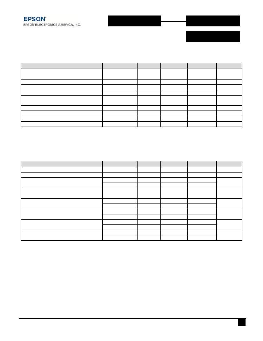
ELECTRICAL CHARACTERISTICS AND SPECIFICATIONS
Absolute Maximum Ratings (For Single Power Supply):
(V
ss
= 0V)
Item
Symbol
Limits
Unit
Power Supply Voltage
V
DD
-0.3 to 4.0
V
Input Voltage
V
I
-0.3 to V
DD
+ 0.5
*1
V
Output Voltage
V
O
-0.3 to V
DD
+ 0.5
*1
V
Output Current/Pin
I
OUT
±
30
mA
Storage Temperature
T
STG
-65 to 150
∞
C
*
1: Possible to use from -0.3V to 7.5V of I/O buffer voltage in the open-drain systems and input buffer in the IDC and IDH
systems.
Absolute Maximum Ratings (For Dual Power Supplies):
(V
ss
= 0V)
Item
Symbol
Limits
Unit
HV
DD
-0.3 to 7.0
V
Power Supply Voltage
LV
DD
-0.3 to 4.0
V
HV
I
-0.3 to HV
DD
+ 0.5
*1
V
Input Voltage
LV
I
-0.3 to LV
DD
+ 0.5
*1
V
HV
O
-0.3 to HV
DD
+ 0.5
*1
V
Output Voltage
LV
O
-0.3 to LV
DD
+ 0.5
*1
V
Output Current/Pin
I
OUT
±
30 (
±
50
*2
)
mA
Storage Temperature
T
STG
-65 to 150
∞
C
**
1: Possible to use from -0.3V to 7.5V of I/O buffer voltage in the open-drain systems and input buffer in the IDC and IDH
systems.
*2: Possible to use for 24mA of output buffer.

4
EPSON ELECTRONICS AMERICA, INC.
i
150 River Oaks Pkwy
i
San Jose, CA 95134
i
Tel: (408) 922-0200
i
Fax: (408) 922-0238
ASIC
S1L50000
DATA SHEET
Recommended Operating Conditions (For Single Power Supplies):
Item
Symbol
Min
Typ
Max
Unit
Power Supply Voltage
V
DD
3.00
3.30
3.60
V
Input Voltage
V
I
V
SS
--
V
DD
*1
V
Ambient Temperature
T
a
0
-40
25
25
70
*2
85
*3
∞
C
Normal Input for Rising Edge Input
t
ri
--
--
50
ns
Normal Input for Falling Edge Input
t
fi
--
--
50
ns
Schmitt Input for Rising Edge Input
t
ri
--
--
5
ms
Schmitt Input for Falling Edge Input
t
fi
--
--
5
ms
*1: Possible to use 5.25 or 5.50V of I/O buffer in the open-drain systems and input buffer in the IDC and IDH systems.
*2: The ambient temperature range is recommended for T
j
= 0 to 80
∞
C
*3: The ambient temperature range is recommended for T
j
= -40 to 125
∞
C
Recommended Operating Conditions (For Single Power Supplies):
Item
Symbol
Min
Typ
Max
Unit
Power Supply Voltage
V
DD
1.80
2.00
2.20
V
Input Voltage
V
I
V
SS
--
V
DD
*1
V
Ambient Temperature
T
a
0
-40
25
25
70
*2
85
*3
∞
C
Normal Input for Rising Edge Input
t
ri
--
--
100
ns
Normal Input for Falling Edge Input
t
fi
--
--
100
ns
Schmitt Input for Rising Edge Input
t
ri
--
--
10
ms
Schmitt Input for Falling Edge Input
t
fi
--
--
10
ms
*1: Possible to use 5.25 or 5.50V of I/O buffer in the open-drain systems and input buffer in the IDC and IDH systems.
*2: The ambient temperature range is recommended for T
j
= 0 to 80
∞
C
*3: The ambient temperature range is recommended for T
j
= -40 to 125
∞
C
5
DATA SHEET
EPSON ELECTRONICS AMERICA, INC.
i
150 River Oaks Pkwy
i
San Jose, CA 95134
i
Tel: (408) 922-0200
i
Fax: (408) 922-0238
ASIC
S1L50000
Recommended Operating Conditions (For Dual Power Supplies):
Item
Symbol
Min
Typ
Max
Unit
Power Supply Voltage (High Voltage)
HV
DD
4.75
4.50
5.00
5.00
5.25
5.50
V
Power Supply Voltage (Low Voltage)
LV
DD
3.00
3.30
3.60
V
HV
I
V
SS
--
HV
DD
Input Voltage
LV
I
V
SS
--
LV
DD
*1
V
Ambient Temperature
T
a
0
-40
25
25
70
*2
85
*3
∞
C
Normal Input for Rising Edge Input
tri
--
--
50
ns
Normal Input for Falling Edge Input
tri
--
--
50
ns
Schmitt Input for Rising Edge Input
tri
--
--
5
ms
Schmitt Input for Falling Edge Input
tri
--
--
5
ms
*1: Possible to use 5.25 or 5.50V of I/O buffer in the open-drain systems and input buffer in the LIDC and LIDH systems.
*2: The ambient temperature range is recommended for T
j
= 0 to 80
∞
C
*3: The ambient temperature range is recommended for T
j
= -40 to 125
∞
C
Recommended Operating Conditions (For Dual Power Supplies):
Item
Symbol
Min
Typ
Max
Unit
Power Supply Voltage (High Voltage)
HV
DD
3.00
3.30
3.60
V
Power Supply Voltage (Low Voltage)
LV
DD
1.80
2.00
2.20
V
HV
I
V
SS
--
HV
DD
Input Voltage
LV
I
V
SS
--
LV
DD
V
Ambient Temperature
T
a
0
-40
25
25
70
*1
85
*2
∞
C
H
tri
--
--
50
Normal Input for Rising Edge Input
L
tri
--
--
100
ns
H
tfi
--
--
50
Normal Input for Falling Edge Input
L
tfi
--
--
100
ns
H
tri
--
--
5
Schmitt Input for Rising Edge Input
L
tri
--
--
10
ms
H
tfi
--
--
5
Schmitt Input for Falling Edge Input
L
tfi
--
--
10
ms
*1: Possible to use 5.25 or 5.50V of I/O buffer in the open-drain systems and input buffer in the LIDC and LIDH systems or HIDC and
HIDH systems.
*2: The ambient temperature range is recommended for T
j
= 0 to 80
∞
C
*3: The ambient temperature range is recommended for T
j
= -40 to 125
∞
C