In pursuit of "Saving" Technology, Epson electronic devices.
Our lineup of semiconductors, liquid crystal displays and quartz devices
assists in creating the products of our customers' dreams.
Epson IS energy savings.
4.5mm
NOTICE
No parts of this material may be reproduced or duplicated in any form or by any means without the written
permission of Seiko Epson. Seiko Epson reserves the right to make changes to this material without notice.
Seiko Epson does not assume any liability of any kind aristing out of any inaccuracies contained in this
material or due to its application or use in any product or circuit and, further, there is no representation that
this material is applicable to products requiring high level reliability, such as, medical products. Moreover,
no license to any intellectual property rights is granted by implication or otherwise, and there is no
representation or warranty that anything made in accordance with this material will be free from any patent
or copyright infringement of a third party. This material or portions thereof may contain technology or the
subject relating to strategic products under the control of the Foreign Exchange and Foreign Trade Law of
Japan and may require an export licence from teh Ministry of International Trade and Industry or other
approval from another government agency.
� SEIKO EPSON CORPORATION 2001, All rights reserved.
All other product names mentioned herein are trademarks and/or registered trademarkes of their respective
companies.

SPC7281F
0A
EPSON
i
Contents
1. DESCRIPTION .................................................................................................................................................. 1
2. FEATURES ........................................................................................................................................................ 1
3. INTERNAL BLOCK DESCRIPTION .................................................................................................................. 3
3.1 BLOCK DIAGRAM ..................................................................................................................................... 3
3.2 BLOCK DIAGRAM DESCRIPTION ............................................................................................................ 3
4. INTERNAL CONNECTION DIAGRAM .............................................................................................................. 4
5. PIN ASSIGNMENT DIAGRAM .......................................................................................................................... 5
6. PIN DESCRIPTION ........................................................................................................................................... 6
7. FUNCTIONAL DESCRIPTION ........................................................................................................................ 10
7.1 MEMORY MAP ........................................................................................................................................ 10
7.1.1 All Memory Space .......................................................................................................................... 10
7.1.2 IEEE1394LINK/Transaction Controller xCSBUF Area (SRAM) ..................................................... 11
7.2 IEEE1394 PACKET FORMAT ................................................................................................................. 12
7.2.1 Transmit Packet Format ................................................................................................................ 12
7.2.2 Receive Packet Format .................................................................................................................. 14
7.3 IEEE1394 HARDWARE SBP-2 CONTROL ............................................................................................. 17
7.4 IDE INTERFACE CONTROL ................................................................................................................... 17
7.5 BUILT-IN CPU .......................................................................................................................................... 17
7.6 FLASH CONTROLLER ............................................................................................................................ 18
8. INTERNAL REGISTER .................................................................................................................................... 19
8.1 IEEE1394 LINK CONTROLLER REGISTER MAPPING ......................................................................... 19
8.1.1 Register Table ............................................................................................................................... 19
8.1.2 Register/Bit Table .......................................................................................................................... 22
8.1.3 Register Map ................................................................................................................................. 26
8.1.4 Detail Description of Register ........................................................................................................ 42
8.2 FLASH ROM CONTROL REGISTER ...................................................................................................... 88
9. ELECTRICAL CHARACTERISTICS ................................................................................................................ 91
9.1 ABSOLUTE MAXIMUM RATINGS ........................................................................................................... 91
9.2 RECOMMENDED OPERATING CONDITION ......................................................................................... 91
9.3 DC CHARACTERISTICS (ACCORDING TO RECOMMENDED OPERATING CONDITION) ................ 92
9.4 AC CHARACTERISTICS ......................................................................................................................... 94
9.4.1 Clock Timing .................................................................................................................................. 94
9.4.2 PHY-LINK Interface Timing ........................................................................................................... 95
9.4.3 IDE Interface Timing ...................................................................................................................... 96
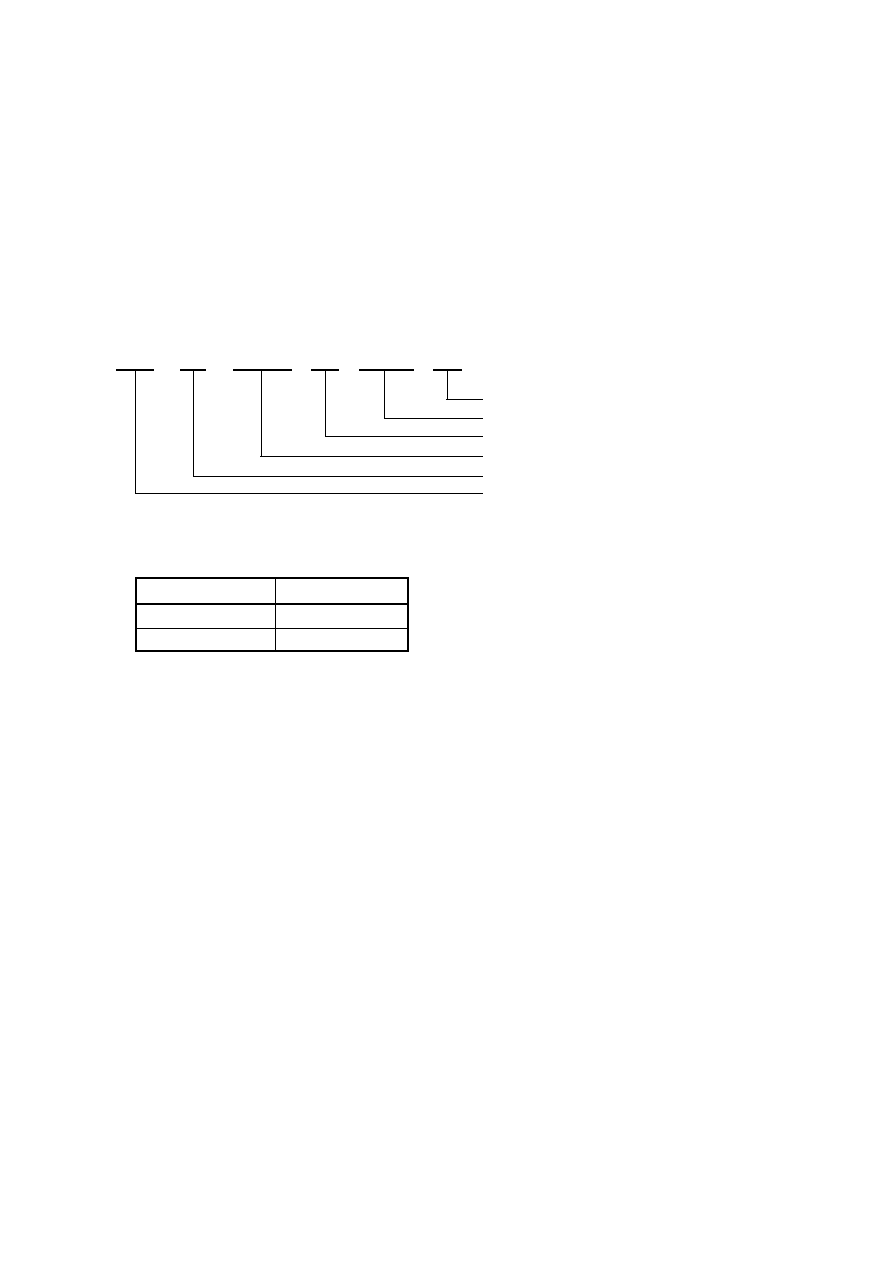
9.4.4 CPU Interface Timing .................................................................................................................. 102
10. EXAMPLES OF EXTERNAL CONNECTION FOR REFERENCE PURPOSES ........................................... 103
11. SHAPE OF PACKAGE .................................................................................................................................. 106

S1R72801F00A
EPSON
1
1. DESCRIPTION
The S1R72801F00A is a LINK/Transaction controller
based on the IEEE Std. 1394-1955, P1394a Draft 2.0. It
integrates a built-in CPU and Flash ROM, and also
integrates a part of transaction functions into hardware.
If you set a PageTable address and its size, it can
automatically fetch subsequent PageTables and transmit
data. It can offer a 1394 interface optimum to computer
peripherals in combination with the Cable PHY
Transceiver Arbiter based on the above standard.
2. FEATURES
q LINK/Transaction Controller
LINK Layer
Ready for all two-way data transfer in Asynchronous
and Isochronous modes.
The built-in SRAM realized stable two-way data
transfer up to max. payload of 100Mbps, 200Mbps,
and 400Mbps.
Can automatically detect the Isochronous Resource
Manager by hardware.
Transaction Layer
Integrates a part of transaction functions into hardware
to prevent deterioration of actual data transmission
rate due to the overhead of firmware (assure a special
area).
A header area is distinguished from a data area to
simplify communications with a higher rank layer.
Furthermore, it segments a data area to a stream area
and ORB area.
Adopts a ring buffer to the receive header area,
receive data area (receive stream area, receive ORB
area) and transmit data area (transmit stream area).
Can arbitrarily set the size of each area.
Automatically controls the Busy when hardware
receives data.
q SBP-2 Support
Can set an PageTable address and its size for the
SBP-2 to automatically perform subsequent Page
Table fetches and data transfers.
q PHY/LINK Interface
Ready for the P1394a.
Ready for the data transfer rate of 100/200/400Mbps.
Ready for isolation (bus holder integrated)
q IDE Interface
Ready for the PIO mode 0/1/2/3/4, multi-word DMA
mode 0/1/2, Ultra-DMA mode 0/1/2.
Usable as a general port interface as well.