SED1670
1
PF836-02
Dot Matrix High Duty LCD Driver
SED1670
s
OVERVIEW
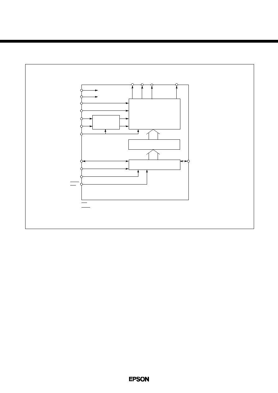
The SED1670 is a 100 output low-power resistance common (row) driver which is suitable for driving a very high
capacity dotmatrix LCD panels upto a duty ratio of 1/300. It is intended to be used in conjunction with the SED1640D
or SED1606D as a pair.
Since the SED1670 is so designed to drive LCDs over a wide range of voltages, and also the maximum potential
V0 of its LCD drive bias voltages is isolated from V
DD
to allow the LCD driving bias voltages to be externally
generated optionally with a high accuracy, it can cope with a wide range of LCD panels.
Owing to its pad layout which can minimize its PC boards mounting space in addition to its selectable bidirectional
driver output sequence and as many as 100 LCD output segments of high pressure resistance and low output
impedance, it is possible to obtain the highest driver working efficiency for the 1/200 duty panel.
And the SED1670 can display 65 x 132 panel when used as a common driver of RAM buit-in driver, SED1531.
s
FEATURES
q
Number of LCD drive output segments: 100
q
Common output ON resistance: 700
(Typ.)
q
Display duty ratio: 1/64 to 1/300 (Reference)
q
Display capacity: Possible to display 640 x 480 dots when used in combination with SED 1640D or SED1606D.
q
Selectable pin output shift direction
q
No-bias display OFF function (*1*)
q
Instantaneous display blanking enabled by inhibit function (*0*)
q
Adjustable offset bias of LCD power to V
DD
level
q
Wide range of LCD drive voltages: ≠7 V to ≠28 V (Absolute maximum rated voltage: ≠30 V)
q
Logic system power supply: ≠2.7 V to ≠5.5 V
q
Chip packaging
SED1670D
0A
(Al-pad die form)
SED1670D
1A
SED1670D
0B
(Au bump die form)
SED1670D
1B
SED1670T
0A
(TCP die form)
* Under Planning
SED1670T
1A
* Under Planning
q
No radial rays countermeasure taken in designing
q
100 Output
q
1/64 to 1/300 in display duty
q
CMOS High Voltage Resistant Process
SED1670
3
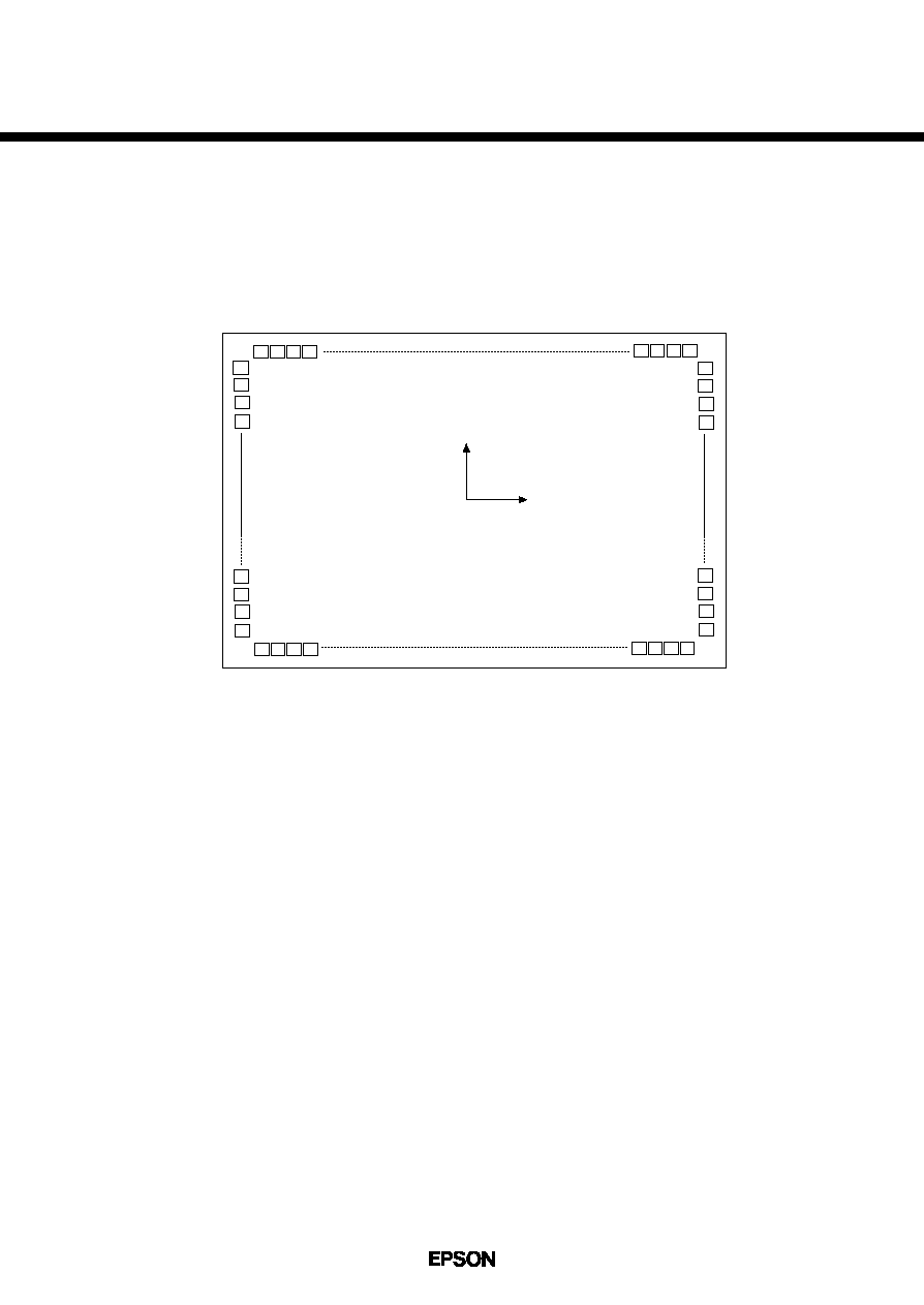
∑ PAD LAYOUT AND COORDINATES
Chip size .............................. 5.49mm x 3.03mm
1) Au bump specification reference values
Bump specific :
High Quarity Au bump
Bump size :
100
µ
m x 113
µ
m
Bump height :
17
µ
m - 28
µ
m
2) Al Pad specification reference values
Pad Opening :
100
µ
m x 100
µ
m
Y
X
112
1
36
37
57
93
56
92
(0,0)
SED1670
5
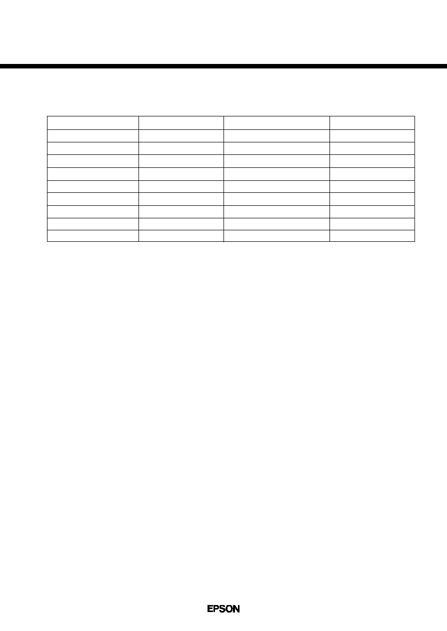
Parameter
Symbol
Rating
Unit
Supply voltage (1)
V
SS
≠7.0 to +0.3
V
Supply voltage (2)
V
5
≠30.0 to +0.3
V
Supply voltage (3)
V
0
, V
1
, V
4
V
5
≠0.3 to +0.3
V
Input voltageV
I
V
SS
≠0.3 to +0.3
V
Output voltage
V
O
V
SS
≠0.3 to +0.3
V
Output current (1)
I
O
20
mA
Output current (2)
I
OCOM
20
mA
Operating temperature
Topr
≠40 to + 85
∞
C
Storing temperature 1
Tstg
≠65 to +150
∞
C
∑ ABSOLUTE MAXIMUM RATINGS
Notes: 1. The voltage of V
0
, V
1
and V
4
must always satisfy the condition of V
DD
>
= V
0
>
= V
1
>
= V
4
>
= V
5
.
2. Floating of the logic system power during while the LCD drive system power is applied, or exceeding
V
SS
= ≠2.6 V or more can cause permanent damage to the LSI. Functional operation under these
conditions is not implied.
Care should be taken to the power supply sequence especially in the system power ON or OFF.
V
DD
=0V