1
SRM20V100LLMX
7
A0 to A16
WE
OE
CS1, CS2
I/O1 to I/O8
V
DD
V
SS
Address Input
Write Enable
Output Enable
Chip Select
Data I/O
Power Supply (2.7V to 3.6V)
Power Supply (0V)
N. C.
No connection
A0
A1
A2
A3
A4
A5
A6
A7
A8
A9
A10
A11
A12
CS1
OE
WE
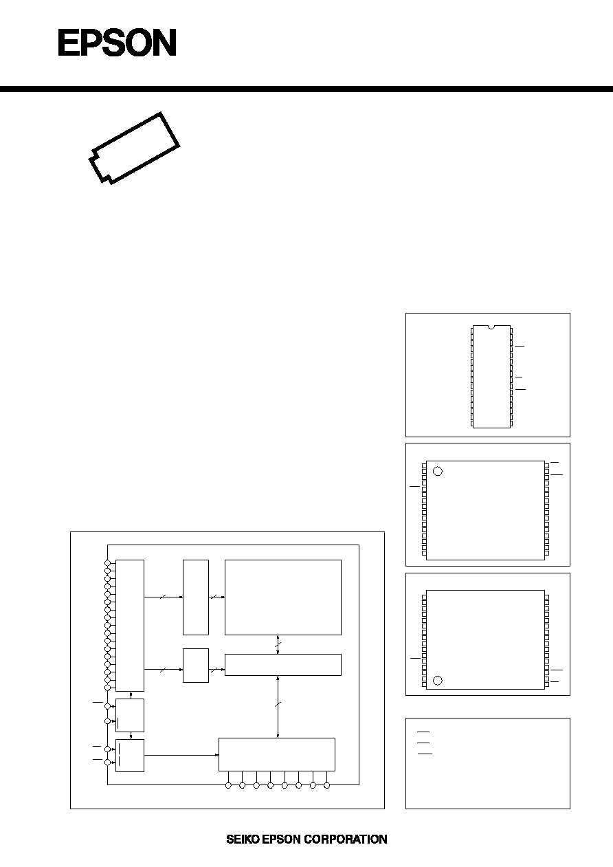
I/O Buffer
Column Gate
Memory Cell Array
1024
◊
128
◊
8
128
◊
8
8
10
1024
7
128
I/O1 I/O2 I/O3 I/O4 I/O5 I/O6 I/O7 I/O8
A13
A15
A16
A14
CS2
Address Buffer
X Decoder
Y
Decoder
Chip
Control
CS1, CS2
Chip
Control
OE, WE
1
A11
32
OE
2
A9
31
A10
3
A8
30
CS1
4
A13
29
I/08
5
WE
28
I/07
6
CS2
27
I/06
7
A15
26
I/05
8
V
DD
25
I/04
9
N.C.
24
V
SS
10
A16
23
I/03
11
A14
22
I/02
12
A12
21
I/01
13
A7
20
A0
14
A6
19
A1
15
A5
18
A2
16
A4
17
A3
16
A4
17
A3
15
A5
18
A2
14
A6
19
A1
13
A7
20
A0
12
A12
21
I/01
11
A14
22
I/02
10
A16
23
I/03
9
N.C.
24
V
SS
8
V
DD
25
I/04
7
A15
26
I/05
6
CS2
27
I/06
5
WE
28
I/07
4
A13
29
I/08
3
A8
30
CS1
2
A9
31
A10
1
A11
32
OE
(SOP6)
(TSOP/Slim-TSOP)
32
V
DD
SRM20V100LLMT
N.C. 1
31
A15
A16
2
30
CS2
A14
3
29
WE
A12
4
28
A13
A7
5
27
A8
A6
6
26
A9
A5
7
25
A11
A4
8
24
OE
A3
9
23
A10
A2
10
22
CS1
A1
11
21
I/08
A0
12
20
I/07
I/01
13
19
I/06
I/02
14
18
I/05
I/03
15
17
I/04
V
SS
16
(TSOP-R1/Slim-TSOP-R1)
SRM20V100LLTX/KX
SRM20V100LLRX/YX
1M-Bit Static RAM
PF805-04
SRM20V100LLMX
7
s
DESCRIPTION
The SRM20V100LLMX
7
is an 131,072 words
◊
8-bit asynchronous, static, random access memory on a monolithic
CMOS chip. Its very low standby power requirement makes it ideal for applications requiring non-volatile storage
with back-up batteries. And --25 to 85
∞
C operating temperature range makes it ideal for portable equipment.
The asynchronous and static nature of the memory requires no external clock or refreshing circuit. Both the
input and output ports are TTL compatible and 3-state output allows easy expansion of memory capacity.
s
FEATURES
q
Wide temperature range ..... ≠25 to 85
∞
C
q
Fast Access time ................. SRM20V100LLMX
7
70ns (Max.)
q
Low supply current .............. standby: 0.6
µ
A (Typ.): LL Version
0.3
µ
A (Typ.): SL Version
operation: 8mA/1MHz (Typ.)
q
Completely static ................. No clock required
q
Supply voltage..................... 2.7V to 3.6V
q
TTL compatible inputs and outputs
q
3-state output with wired-OR capability
q
Non-volatile storage with back-up batteries
q
Package ...... SRM20V100LLMX
7
SOP6-32pin (plastic)
SRM20V100LLTX
7
TSOP (
I
)-32pin (plastic)
SRM20V100LLRX
7
TSOP (
I
)-32pin-R1 (plastic)
SRM20V100LLKX
7
Slim-TSOP (
I
)-32pin (plastic)
SRM20V100LLYX
7
Slim-TSOP (
I
)-32pin-R1 (plastic)
s
BLOCK DIAGRAM
°
PIN DESCRIPTION
Low Voltage
Operation
Products
q
Low Supply Voltage
q
Wide Temperature Range
q
Low Supply Current
q
Access Time 70ns (2.7V)
q
131,072 Words
◊
8-Bit Asynchronous
s
PIN CONFIGURATION
2
s
ABSOLUTE MAXIMUM RATINGS
s
DC RECOMMENDED OPERATING CONDITIONS
Supply voltage
Input voltage
Input/Output voltage
Power dissipation
Operating temperature
Storage temperature
Soldering temperature and time
V
DD
V
I
V
I/O
P
D
T
opr
T
stg
T
sol
≠0.5 to 4.6
≠0.5 to V
DD
+0.3
≠0.5 to V
DD
+0.3
0.5
≠25 to 85
≠65 to 150
260
∞
C, 10s (at lead)
Parameter
Symbol
Ratings
Unit
(V
SS
= 0V)
T
VI, VI/O (Min.) = ≠3.0V (Pulse width is 50ns)
V
V
V
W
∞
C
∞
C
--
(V
SS
= 0V, Ta = ≠25 to 85
∞
C)
Parameter
Input voltage
Supply voltage
Symbol
Conditions
V
DD
V
SS
V
IH
V
IL
T
If pulse width is less than 50ns, it is ≠3.0V
--
--
--
--
Min.
2.7
0
2.2
≠0.3
T
Typ.
3.0
0
--
--
Max.
3.6
0
V
DD
+0.3
0.4
V
V
V
V
Unit
Parameter
Symbol
Conditions
Unit
Input leakage
High level output voltage
Low level output voltage
Operating supply current
Average operating current
I
LI
V
OH
V
OL
I
DDS
I
DDO
µ
A
mA
V
(V
DD
= 2.7 to 3.6V, V
SS
= 0V, Ta = ≠25 to 85
∞
C)
I
DDA
T
Typical values are measured at Ta=25
∞
C and V
DD
=3.0V
V
I
=0 to V
DD
CS1 = V
IH
or CS2 = V
IL
V
µ
A
mA
Standby supply current
I
DDS1
I
DDA1
CS1 = CS2
V
DD
--0.2V
or CS2
0.2V
V
I
= V
IL
, V
IH
I
I/O
= 0mA, t
cyc
= Min.
V
I
= V
IL
, V
IH
I
I/O
= 0mA, t
cyc
= 1
µ
s
V
I
= V
IL
, V
IH
I
I/O
= 0mA
mA
mA
≠1
Min.
Typ.
T
Max.
2.4
V
DD
--0.2
--
--
--
LL
SL
--
--
--
--
--
--
--
--
--
0.6
0.3
20
8
8
--
--
1
--
--
1.0
60
30
35
15
15
0.4
0.2
V
DD
3V, I
OH
= ≠2.0mA
I
OH
= ≠100
µ
A
V
DD
3V, I
OL
= ≠2.0mA
I
OL
= 100
µ
A
(f = 1MHz, Ta = 25
∞
C)
Parameter
Symbol
Address Capacitance
Input Capacitance
I/O Capacitance
C
ADD
C
I
C
I/O
Min.
Typ.
Max.
Unit
Conditions
pF
pF
pF
V
ADD
=0V
V
I
=0V
V
I/O
=0V
8
8
10
--
--
--
--
--
--
Output leakage
I
LO
µ
A
CS1 = V
IH
or CS2 = V
IL
or WE = V
IL
or OE = V
IH
, V
IO
= 0 to V
DD
≠1
--
1
s
ELECTRICAL CHARACTERISTICS
q
DC Electrical Characteristics
q
Terminal Capacitance

3
SRM20V100LLMX
7
Unit
ns
ns
ns
ns
ns
ns
ns
ns
ns
ns
ns
ns
70
--
--
--
--
5
--
5
--
0
--
10
Min.
Max.
--
70
70
70
40
--
30
--
30
--
30
--
Parameter
Symbol
Conditions
(V
DD
= 2.7V to 3.6V, V
SS
= 0V, Ta = ≠25 to 85
∞
C)
Read cycle time
Address access time
Chip select1 access time
Chip select2 access time
Output enable access time
Chip select1 output set time
Chip select1 output floating
Chip select2 output set time
Chip select2 output floating
Output enable output set time
Output enable output floating
Output hold time
t
RC
t
ACC
t
ACS1
t
ACS2
t
OE
t
CLZ1
t
CHZ1
t
CLZ2
t
CHZ2
t
OLZ
t
OHZ
t
OH
T
1
T
2
T
1
Unit
ns
ns
ns
ns
ns
ns
ns
ns
ns
ns
ns
70
60
60
60
0
55
0
30
0
--
5
Min.
Max.
--
--
--
--
--
--
--
--
--
30
--
Parameter
Symbol
Conditions
(V
DD
= 2.7V to 3.6V, V
SS
= 0V, Ta = ≠25 to 85
∞
C)
Write cycle time
Chip select time1
Chip select time2
Address enable time
Address setup time
Write pulse width
Address hold time
Input data setup time
Input data hold time
WE Output floating
WE Output setup time
t
WC
t
CW1
t
CW2
t
AW
t
AS
t
WP
t
WR
t
DW
t
DH
t
WHZ
t
OW
T
1
T
2
+3V
1.0k
920
C
L
I/O
C
L
=5pF (Includes Jig Capacitance)
+3V
1.0k
920
C
L
I/O
C
L
=100pF (Includes Jig Capacitance)
T
1 Test Conditions
1. Input pulse level: 0.4V to 2.4V
2. t
r
= t
f
= 5ns
3. Input and output timing reference
levels : 1.5V
4. Output load C
L
= 100pF
T
2 Test Conditions
1. Input pulse level : 0.4V to 2.4V
2. t
r
= t
f
= 5ns
3. Input timing reference levels: 1.5V
4. Output timing reference levels:
±
200mV (the level displaced from
stable output voltage level)
5. Output load C
L
= 5pF
q
AC Electrical Characteristics
r
Read Cycle
r
Write Cycle
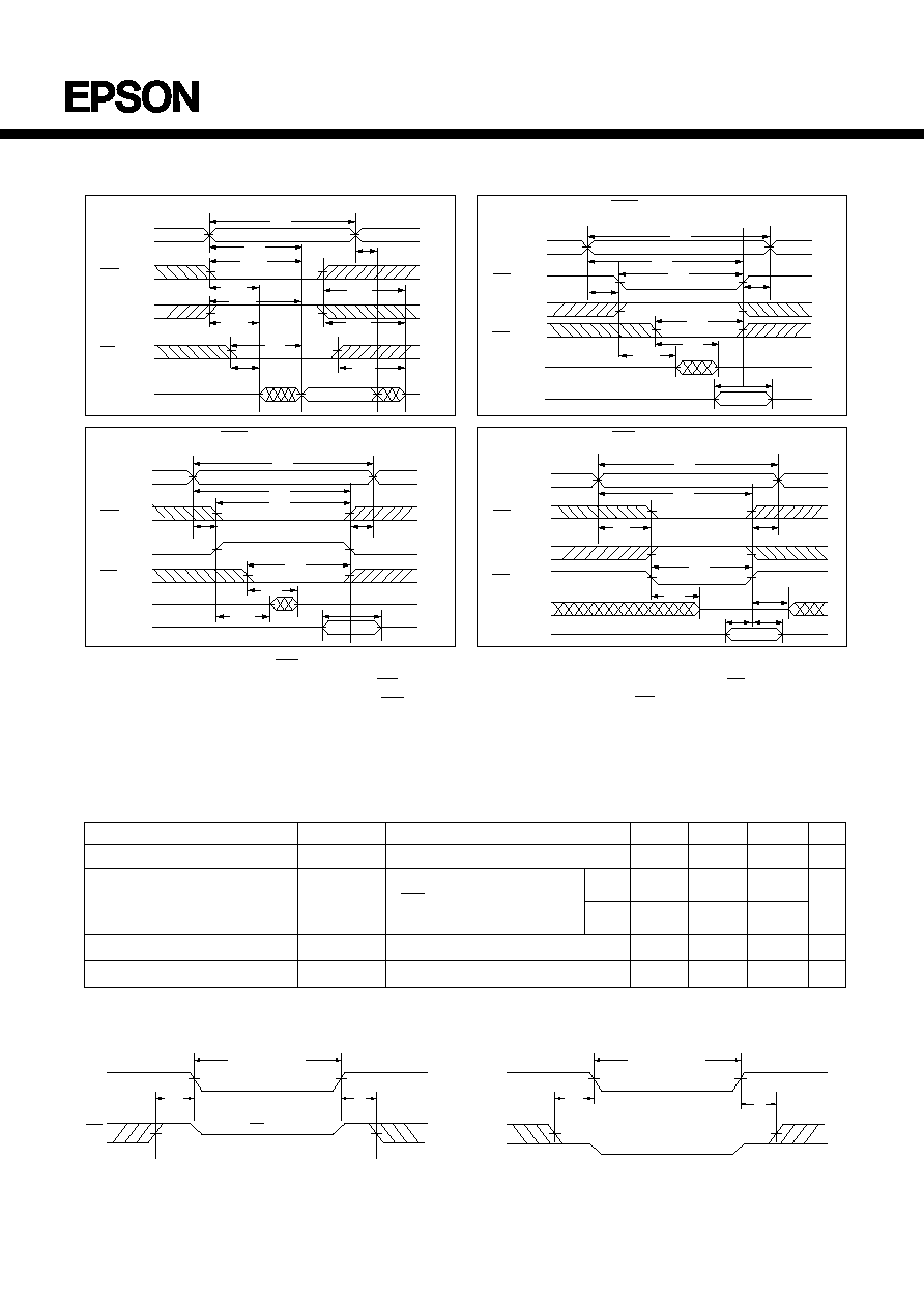
4
Note : 1. During read cycle time, WE is to be "H" level.
2. During write cycle time that is controlled by CS1 or CS2, Output Buffer is in high impedance state, whether OE level is "H" or "L".
3. During write cycle time that is controlled by WE, Output Buffer is high impedance state if OE is "H" level.
4. When I/O terminals are output mode, be careful that do not give the opposite signals to the I/O terminals.
r
Write Cycle (3) (WE Control)
T
3,
T
4
Address
CS1
CS2
WE
Dout
Din
t
WC
t
AW
t
WP
t
DW
t
WR
t
AS
t
WHZ
t
OW
t
DH
r
Write Cycle (2) (CS2 Control)
T
2
Address
CS1
CS2
WE
Dout
Din
t
WC
t
AW
t
WP
t
CW2
t
CLZ2
t
WHZ
t
DW
t
WR
t
AS
t
DH
r
Read Cylcle
T
1
Address
CS1
CS2
OE
Dout
r
Write Cycle (1) (CS1 Control)
T
2
Address
CS1
CS2
WE
Dout
Din
t
WC
t
AW
t
WR
t
CW1
t
WHZ
t
CLZ1
t
DW
t
WR
t
AS
t
DH
t
OH
t
CHZ1
t
ACS2
t
CLZ2
t
CHZ2
t
OE
t
OHZ
t
OLZ
t
RC
t
ACC
t
ACS1
t
CLZ1
q
Timing chart
T
when retaining data in standby mode, supply voltage can be lowered with in a certain range. But read or write cycle
cannot be performed while the supply voltage is low.
q
DATA RETENTION CHARACTERISTIC WITH LOW VOLTAGE POWER SUPPLY
Parameter
Symbol
Conditions
Min.
Typ.
Max.
Unit
Data retention Supply voltage
Data retention current
Chip select data hold time
V
DDR
I
DDR
t
CDR
2.0
3.6
50
V
ns
(V
SS
= 0V, Ta = ≠25 to 85
∞
C)
0
5
Operation recovery time
t
R
ms
V
DD
= 2.7V
CS1 = CS2
V
DD
--0.2V
or CS2
0.2V
T
Ta = 25
∞
C
0.5
T
--
LL
25
0.25
T
--
SL
µ
A
--
--
--
--
--
V
DD
CS2
t
CDR
t
R
V
IL
V
IL
V
DDR
2.0V
CS2
0.2V
Data hold mode
Data retention timing (CS1 Control)
2.7V
2.7V
V
DD
CS1
t
CDR
V
IH
t
R
V
IH
V
DDR
2.0V
CS1
V
DD
--0.2V
Data hold mode
2.7V
2.7V
Data retention timing (CS2 Control)
5
SRM20V100LLMX
7
q
Reading data
Data is able to be read when the address is set while holding CS1 = "L", CS2 = "H", OE = "L" and WE = "H".
Since DATA I/O terminals are in high impedance state when OE = "H", the data bus line can be used for any
other objective, then access time apparently is able to be cut down.
q
Writing data
There are the following four ways of writing data into the memory.
(1) Hold CS2 = "H", WE = "L", set addresses and give "L" pulse to CS1.
(2) Hold CS1 = "L", WE = "L" ,set addresses and give "H"pulse to CS2.
(3) Hold CS1 = "L", CS2 = "H", set addresses and give "L" pulse to WE.
(4) After setting addresses, give "L" pulse to CS1, WE and give "H" pulse to CS2.
Anyway, data on the Data I/O terminals are latched up into the SRM20V100LLMX
7
at the end of the period that
CS1, WE are "L" level, and CS2 is "H" level. As Data I/O terminals are in high impedance state when any of
CS1, OE = "H", or CS2 = "L", the contention on the data bus can be avoided.
q
Standby mode
When CS1 is "H" or CS2 is "L" level, the SRM20V100LLMX
7
is in the standby mode which has retaining data
operation. In this case Data I/O terminals are Hi-Z, and all inputs of addresses, WE and data can be any "H" or
"L". When CS1 and CS2 level are in the range over V
DD
-0.2V, CS2 level is in the range under 0.2V, in the
SRM20V100LLMX
7
there is almost no current flow except through the high resistance parts of the memory.
s
FUNCTIONS
q
Truth Table
X : "H" or "L"
H
X
L
L
L
CS1
X
L
H
H
H
CS2
X
X
X
L
H
X
X
L
H
H
OE
WE
DATA I/O
I
DD
Mode
I
DDS,
I
DDS1
I
DDS,
I
DDS1
I
DDO
I
DDO
I
DDO
Hi-Z
Hi-Z
Input data
Output data
Hi-Z
Unselected
Unselected
Write
Read
Output disable
6
s
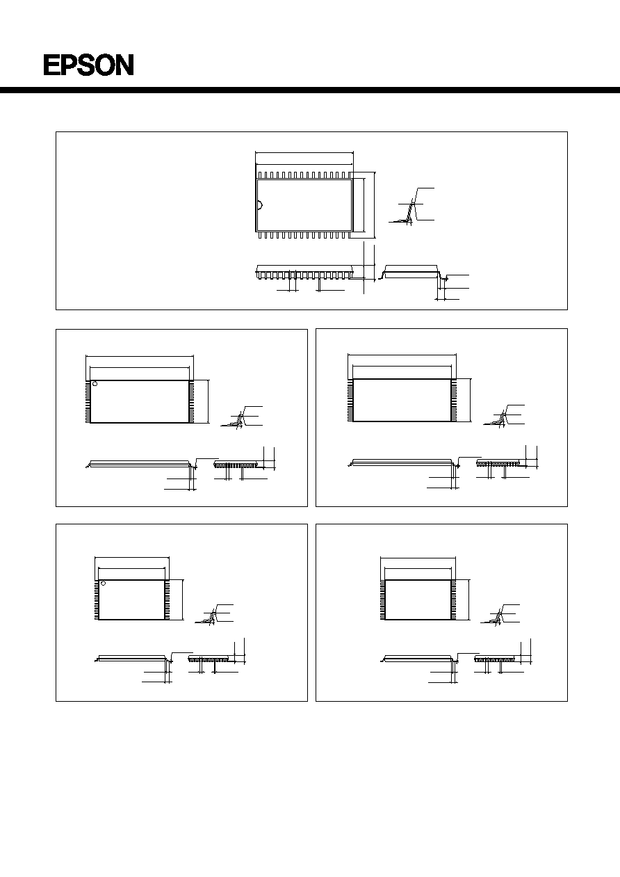
PACKAGE DIMENSIONS
Unit : mm
(inch)
Plastic SOP6-32pin
17
32
16
1
1.27
(0.05)
20.45
±
0.1
(0.805 )
11.295
±
0.1
(
0.445
)
+0.003 ≠0.004
0.4
±
0.1
(0.016 )
+0.003
≠0.004
3.1
max
(
0.122
max
)
+0.004
≠0.003
0.2
(
0.008
)
1.42
(0.056)
0
∞
8
∞
0.15
±
0.05
(0.006 )
+0.001
≠0.002
20.85
max
(0.82
max
)
14.135
±
0.3
(
0.556
)
+0.012 ≠0.011
2.7
±
0.1
(
0.106
)
+0.004 ≠0.003
0.8
±
0.2
(0.031 )
+0.008
≠0.007
Plastic TSOP (
I
) -32pin
Unit : mm
(inch)
32
1
17
16
INDEX
18.4
±
0.2
(0.724 )
+0.008
≠0.007
0
∞
10
∞
8
±
0.2
(
0.315
±
0.007
)
20
±
0.2
(0.787 )
+0.008
≠0.007
0.5
±
0.1
(0.02 )
+0.003
≠0.004
0.15
(0.006 )
+0.002
≠0.003
0.5
(0.02)
1.27
max
(
0.05
max
)
0.2
±
0.1
(0.008 )
+0.003
≠0.004
1
(
0.039
)
+0.07
≠0.075
0.8
±
0.2
(0.031 )
+0.008
≠0.007
Unit : mm
(inch)
Plastic Slim-TSOP (
I
) -32pin
Plastic TSOP (
I
) -32pin-R1
Unit : mm
(inch)
Unit : mm
(inch)
Plastic Slim-TSOP (
I
) -32pin-R1
17
16
32
1
18.4
±
0.2
(0.724 )
+0.008
≠0.007
0
∞
10
∞
8
±
0.2
(
0.315
±
0.007
)
20
±
0.2
(0.787 )
+0.008
≠0.007
0.5
±
0.1
(0.02 )
+0.003
≠0.004
0.15
(0.006 )
+0.002
≠0.003
0.5
(0.02)
1.27
max
(
0.05
max
)
0.2
±
0.1
(0.008
)
+0.003
≠0.004
1
(
0.039
)
+0.07
≠0.075
0.8
±
0.2
(0.031 )
+0.008
≠0.007
INDEX
32
1
17
16
INDEX
11.8
±
0.1
(
0.465
±
0.003
)
0
∞
10
∞
8
±
0.2
(
0.315
±
0.007
)
13.4
±
0.3
(
0.528
±
0.011
)
0.5
±
0.1
(
0.02
)
+0.003
≠0.004
0.15
(
0.006
)
+0.002
≠0.003
0.5
(
0.02
)
1.27
max
(
0.05
max
)
0.2
±
0.1
(
0.008
)
+0.003
≠0.004
1
(
0.039
)
+0.07
≠0.075
0.8
±
0.2
(
0.031
)
+0.008
≠0.007
17
16
32
1
11.8
±
0.1
(
0.465
±
0.003
)
0
∞
10
∞
8
±
0.2
(
0.315
±
0.007
)
13.4
±
0.3
(
0.528
±
0.011
)
0.5
±
0.1
(
0.02
)
+0.003
≠0.004
0.15
(
0.006
)
+0.002
≠0.003
0.5
(
0.02
)
1.27
max
(
0.05
max
)
0.2
±
0.1
(
0.008
)
+0.003
≠0.004
1
(
0.039
)
+0.07
≠0.075
0.8
±
0.2
(
0.031
)
+0.008
≠0.007
INDEX

7
SRM20V100LLMX
7
s
CHARACTERISTICS CURVES
1.7
1.6
1.5
1.4
1.3
1.2
1.1
1
0.9
0.8
0.7
0.6
≠40 ≠20
0
20
40
60
80
WRITE
V
DD
= 3.0V
READ, WRITE
READ
Ta (
∞
C)
1
0.9
0.8
0.7
0.6
0.5
0.4
0.3
0.2
0.1
0
20
18
16
14
12
10
8
6
4
2
0
Frequency (MHz)
1/t
RC
, 1/t
WC
1.6
1.5
1.4
1.3
1.2
1.1
1
0.9
0.8
0.7
0.6
2.4
2.7
3
3.3
3.6
3.9
V
DD
(V)
0
0.2
0.4
0.6
0.8
1
1.2
1.4
1.6
1.8
2
2.2
2.4
0.5
1
1.5
2
2.5
3
3.5
V
OH
(V)
Normalized I
DDA
--Ta
Normalized I
DDA
--V
DD
Normalized I
DDA
--Frequency
Normalized I
DDS1
--V
DD
Normalized I
OH
--V
OH
100
10
1
0.1
0.01
80
60
40
20
0
≠20
≠40
Ta (
∞
C)
100
1
0.1
3.9
3.6
3.3
3
2.7
2.4
V
DD
(V)
Normalized I
DDS1--
Ta
V
DD
= 3.0V
Ta = 25
∞
C
V
DD
= 3.0V
WRITE
READ
Ta = 25
∞
C
Ta = 25
∞
C
READ, WRITE
WRITE
READ
Ta = 25
∞
C
V
DD
= 3.0V
8
IC Marketing & Engineering Group
421≠8 Hino, Hino≠shi, Tokyo 191, JAPAN
Phone: 0425≠87≠5816
FAX: 0425≠87≠5624
International Marketing Department I (Europe & U. S. A.)
421-8 Hino, Hino-shi, Tokyo 191, JAPAN
Phone: 0425≠87≠5812
FAX: 0425≠87≠5564
International Marketing Department II (Asia)
421-8 Hino, Hino-shi, Tokyo 191, JAPAN
Phone: 0425≠87≠5814
FAX: 0425≠87≠5110
ELECTRONIC DEVICE MARKETING DEPARTMENT
First issue Oct. 1995, printed Feb. 1997 in Japan T
© Seiko Epson Corporation 1996 All right reserved.
NOTICE:
No part of this material may be reproduced or duplicated in any form or by any means without the written permission of Seiko Epson. Seiko Epson
reserves the right to make changes to this material without notice. Seiko Epson does not assume any liability of any kind arising out of any
inaccuracies contained in this material or due to its application or use in any product or circuit and, further, there is no representation that this material
is applicable to products requiring high level reliability, such as, medical products. Moreover, no license to any intellectual property rights is granted
by implication or otherwise, and there is no representation or warranty that anything made in accordance with this material will be free from any
patent or copyright infringement of a third party. This material or portions thereof may contain technology or the subject relating to strategic products
under the control of the Foreign Exchange and Foreign Trade Control Law of Japan and may require an export license from the Ministry of
International Trade and Industry or other approval from another government agency.
SRM20V100LLMX
7
0
0.2
0.4
0.6
0.8
1
1.2
1.4
1.6
1.8
2
2.2
0
0.2
0.4
0.6
0.8
1
V
OL
(V)
Normalized t
ACS1
--Ta
t
ACC
t
ACS2
Normalized t
ACS1
--V
DD
t
ACC
t
ACS2
Normalized t
ACS1
--C
L
t
ACC
t
ACS2
Normalized I
DDR
--Ta
Normalized I
OL
--V
OL
1.4
1.3
1.2
1.1
1.0
0.9
0.8
0.7
Ta (
∞
C)
1.3
1.25
1.2
1.15
1.1
1.05
1
0.95
0.9
0.85
0.8
V
DD
(V)
3.9
3.6
3.3
3
2.7
2.4
80
60
40
20
0
≠20
≠40
V
DD
= 3.0V
Ta = 25
∞
C
Ta = 25
∞
C
V
DD
= 3.0V
2.2
2.1
2.0
1.9
1.8
1.7
1.6
1.5
1.4
1.3
1.2
1.1
1
0.9
0.8
0.7
0.6
0.5
0
100
200
300
400
C
L
(pF)
100
10
1
0.1
0.01
≠40 ≠20
0
20
40
60
80
Ta (
∞
C)
Ta = 25
∞
C
V
DD
= 3.0V
V
DD
=2.7V