 | –≠–ª–µ–∫—Ç—Ä–æ–Ω–Ω—ã–π –∫–æ–º–ø–æ–Ω–µ–Ω—Ç: PBL3776-1 | –°–∫–∞—á–∞—Ç—å:  PDF PDF  ZIP ZIP |

24-pin plastic DIP package, narrow
PBL 3776/1
Dual Controller IC for High Current
Stepper Motor Applications
Description
The PBL 3776/1 is a switch-mode (chopper), constant-current controller IC intended
for controlling external transistors in a high current stepper motor application.The IC
has two channels one for each winding of a two-phase stepper motor. The circuit is
similar to Ericsson¥s PBL 3775/1. PBL 3776/1 is equipped with a Disable input to
simplify half-stepping operation.
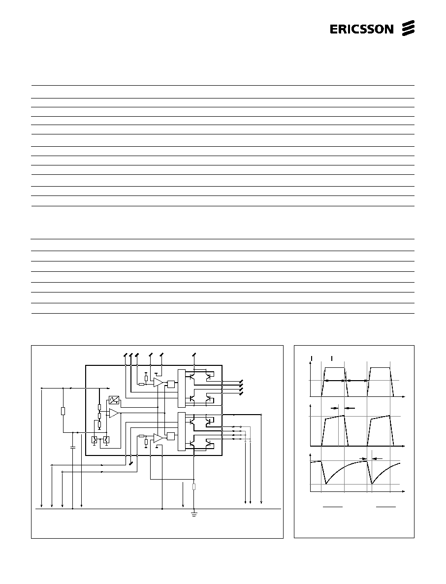
The PBL 3776/1 contains a clock oscillator, which is common for both driver
channels, a set of comparators and flip-flops implementing the switching control, and
two output sections each containing four outputs, two source and two sink, intended
to drive an external H-bridge.
Voltage supply requirements are +5 V for logic and +10 to +45 V for the outputs.
The close match between the two driver channels guarantees consistent output
current ratios and motor positioning accuracy.
Figure 1. Block diagram.
Key Features
∑
Suitable to drive any external Mos Fet
or bipolar power transistor.
∑
0
∞
C to +85
∞
C operation.
∑
Few external components.
∑
Crossconduction prevented by time
delay.
∑
Close matching between channels for
high positioning accuracy.
∑
Digital filter on chip eliminates
external
filtering components.
∑
Plastic 24-pin "narrow" DIP package.
PBL3776/1
RC
PBL 3776/1
V
CC
V
CC
S
R
Q
Logic
S
R
Q
+
≠
+
≠
+
≠
Logic
V
R2
V
BB1
T
1BU
Phase 2
Phase 1
Dis2
C2
SGND 2
Pwr GND 2
1BL
T
1AU
T
1AL
T
BB2
V
T
2BU
2AU
T
2AL
T
2BL
T
V
R1
Dis 1
C1
SGND 1
Pwr GND 1
1
February 1999
1
PBL 3776/1
2
Figure 3. Definition of terms.
Figure 2. Definition of symbols and test circuit.
Maximum Ratings
Parameter
Pin no.*
Symbol
Min
Max
Unit
Voltage
Logic supply
13
V
CC
0
7
V
Output supply
6, 19
V
BB
0
45
V
Logic inputs
10, 11, 14, 15
V
I
-0.3
6
V
Analog inputs
8, 9, 16, 17
V
A
-0.3
V
CC
V
Current
Output current t=1mS
2, 3, 4, 5, 20, 21, 22, 23
I
O
-500
+500
mA
Logic inputs
10, 11, 14, 15
I
I
-10
mA
Analog inputs
8, 9, 16, 17
I
A
-10
mA
Temperature
Junction temperature
T
J
+150
∞
C
Storage temperature
T
S
-55
+150
∞
C
Recommended Operating Conditions
Parameter
Symbol
Min
Typ
Max
Unit
Logic supply voltage
V
CC
4.75
5
5.25
V
Supply voltage
V
BB
10
40
V
Output emitter voltage
V
E
1.0
V
Output current continuous (see text)
I
M
-200
+200
mA
Operating ambient temperature
T
A
0
+85
∞
C
Rise and fall time logic inputs
t
r,
, t
f
2
µ
s
Oscillator timing resistor
R
T
2
12
20
kohm
* For test purposes only
V
CH
t
d
t
50 %
t
on
t
off
t
t
V
RC
t
b
V
C
f =
s
ton toff
+
1
D =
t
t
on
off
+
t
on
V
OA
V
OB
-
ICC
IA
4 700 pF
VCC
V
V
V
I
IH
IL
V
V
A
R
V
V
V
CH
C
A
VBB
R T
12 k
C
T
IR
V
RC
IRC
VOA
RC
PBL 3776/1
V
CC
V
CC
S
R
Q
Logic
S
R
Q
+
≠
+
≠
+
≠
Logic
VR2
VBB1
T1BU
Phase 2
Phase 1
Dis2
C2
SGND 2
Pwr GND 2
1BL
T
1AU
T
1AL
T
BB2
V
T2BU
2AU
T
2AL
T
2BL
T
VR1
Dis 1
C1
SGND 1
Pwr GND 1
II
IH
I
IL
I
VOB
24
18
23
21
20
22
19
16
17
14
15
12
13
10
11
8
9
7
1
2
4
5
3
6
OU
I
I
OL
I
OL
OU
I
*
*
Rs
I
BB

PBL 3776/1
3
Electrical Characteristics
Electrical characteristics over recommended operating conditions, unless otherwise noted. 0
∞
C
T
j
+125
∞
C.
Ref.
Parameter
Symbol fig.
Conditions
Min
Typ
Max
Unit
General
Supply current
I
CC
2
Note 3.
65
70
mA
Supply current
I
CC
2
Dis
1
= Dis
2
= HIGH.
7
10
mA
Total power dissipation
P
D
V
BB
= 24 V, I
BB1
= I
BB2
= 200 mA.
0.2
0.3
W
Notes 2, 3.
Thermal shutdown junction temperature
Note 2
160
∞
C
Turn-off delay
t
d
3
T
A
= +25
∞
C, dV
C
/dt
50 mV/
µ
s,
1.1
2.0
µ
s
I
BB
= 100 mA. Note 2.
Logic Inputs
Logic HIGH input voltage
V
IH
2
2.0
V
Logic LOW input voltage
V
IL
2
0.6
V
Logic HIGH input current
I
IH
2
V
I
= 2.4 V
20
µ
A
Logic LOW input current
I
IL
2
V
I
= 0.4 V
-0.2
-0.1
mA
Analog Inputs
Input current
I
A
2
V
r
= 5 V
0.5
0.8
mA
|V
C1
--V
C2
| mismatch
V
Cdiff
2
T
A
= 25
∞
C Note 3
5
mV
Motor Outputs
Lower transistor saturation voltage
8
I
M
= 200 mA
0.2
0.4
V
Lower transistor leakage current
2
Dis1 = Dis2 = High, T
A
= 25
∞
C
50
µ
A
Upper transistor saturation voltage
9
I
M
= 200 mA
0.9
1.2
V
Upper transistor leakage current
2
Dis1 = Dis2 = High, T
A
= 25
∞
C
50
µ
A
Chopper Oscillator
Chopping frequency
f
s
3
C
T
= 4 700 pF, R
T
= 12 kohm
23.0
kHz
Digital filter blanking time
t
b
3
C
T
= 4 700 pF. Note 3.
1.0
µ
s
Thermal Characteristics
Ref.
Parameter
Symbol fig.
Conditions
Min
Typ
Max
Unit
T
J-A
R
thJ-C
Note 2
28
∞
C/W
T
J-A
R
thJ-A
Note 2
45
∞
C/W
Notes
1. All voltages are with respect to ground. Currents are positive into, negative out of specified terminal.
2. Not covered by final test program.
3. Switching duty cycle D = 30%, f
s
= 23.0 kHz.

PBL 3776/1
4
Pin Description
DIP
Symbol
Description
1
PWR GND
1
"Power Ground" from output channel 1. Connected to the ground path (see application examples).
2
T1BL
Output, channel 1, B side lower transistor. The pin will sink current when phase is high.
3
T1BU
Output, channel 1, B side upper transistor. The pin will source current when phase is low.
4
T1AL
Output, channel 1, A side lower transistor. The pin will sink current when phase is low.
5
T1AU
Output, channel 1, A side upper transistor. The pin will source current when phase is high.
6
VBB1
Supply voltage for driving channel 1 outputs.
7
SGND
1
Sense ground channel 1. Logic ground reference and sense ground for the current control feedback-
loop.
8
VR
1
Reference voltage, channel 1. Controls the comparator threshold voltage and hence the output
current.
9
C
1
Comparator input channel 1. This input senses the instantaneous voltage across the sensing resistor,
filtered by the internal digital filter or an optional external RC network.
10
Phase
1
Controls the direction of channel 1 outputs T1AL, T1AU, T1BL and T1BU.
11
Dis
1
Disable input for channel 1. When HIGH, all four output transistors are turned off, which results in a
rapidly decreasing output current to zero.
12
RC
Clock oscillator RC pin. Connect a 12 kohm resistor to V
CC
and a 4 700 pF capacitor to ground to
obtain the nominal switching frequency of 23.0 kHz and a digital filter blanking time of 1.0
µ
s.
13
Vcc
Logic voltage supply, nominally +5 V.
14
Dis
2
Disable input for channel 2. When HIGH, all four output transistors are turned off, which results in a
rapidly decreasing output current to zero.
15
Phase
2
Controls the direction of channel 2 outputs T2AL, T2AU, T2BL and T2BU.
16
C
2
Comparator input channel 2. This input senses the instantaneous voltage across the sensing resistor,
filtered by the internal digital filter or an optional external RC network.
17
VR
2
Reference voltage, channel 2. Controls the comparator threshold voltage and hence the output
current.
18
SGND
2
Sense ground channel 1. Logic ground reference and sense ground for the current control feedback-
loop.
19
VBB2
Supply voltage for driving channel 2 outputs.
20
T2AU
Output, channel 2, A side upper transistor. The pin will source current when phase is high.
21
T2AL
Output, channel 2, A side lower transistor. The pin will sink current when phase is low.
22
T2BU
Output, channel 2, B side upper transistor. The pin will source current when phase is low.
23
T2BL
Output, channel 2, B side lower transistor. The pin will sink current when phase is high.
24
PWR GND
2
"Power Ground" from output channel 2. Connected to the ground path (see application examples).
Figure 4. Pin configuration.
PWR GND
1
T1BL
T1BU
T1AL
T1AU
VBB1
SGND
1
VR
1
C
1
Phase
1
Dis
1
PWR GND
2
T2BL
RC
Vcc
Dis
2
T2AL
T2AU
VBB 2
SGND
2
VR
2
C
2
Phase
2
1
2
3
4
5
6
7
8
9
10
11
24
23
12
13
14
21
20
19
18
17
16
15
22
T2BU
PBL
3776/1

PBL 3776/1
5
Functional Description
Each channel of the PBL 3776/1
consists of the following sections:
∑
An output section with four output
transistors, two sourcing and two
sinking, intended to drive the four
transistors in an external H-bridge.
Each transistor is capable of driving
up to 200 mA continuous current.
∑
A logic section that controls the
output transistors.
∑
An S-R flip-flop, and a comparator.
The clock-oscillator is common to
both channels.
Constant current control is achieved
by switching the output current to the
windings. This is done by sensing the
peak current through the winding via a
current-sensing resistor R
S
, effectively
connected in series with the motor
winding. As the current increases, a
voltage develops across the sensing
resistor, which is fed back to the
comparator. At the predetermined level,
defined by the voltage at the reference
input V
R
, the comparator resets the flip-
flop, which turns off the sourcing output
transistor in the circuit. Consequently the
correspond-ing lower external transistor,
in the H-bridge, is turned off. The turn-off
of one channel is independent of the
other channel. The current decreases
until the clock oscillator triggers the flip-
flops of both channels simultaneously,
which turns on the output transistors
again, and the cycle is repeated.
To prevent erroneous switching due to
switching transients at turn-on, the PBL
3776/1 includes a digital filter. The clock
oscillator provides a blanking pulse
which is used for digital filtering of the
voltage transient across the current
sensing resistor during turn-on. Due to
the high output drive capability, this
transient might exceed the max. allowed
voltage on the C inputs and damage the
circuit. A resistor is placed in the
feedback loop in order to prevent this
transient from damaging the circuit.
The current paths during turn-on, turn-
off and phase shift are shown in figure 6.
Applications Information
Output current
The maximum peak output, sink/source,
current is 500 mA. But due to the power
handling capacity of the package this
Figure 5. Typical 5 A stepper motor driver application with PBL 3776/1. One channel shown.
current can only be used for a short
period of time (1mS). Recommended
max continuous output current is 200
mA/output transistor. This is practical
when driving MOS FET power
transistors, since a high peak output
current capability will rapidly charge/
discharge the gate capacitance, while
the continuous current usage is very
small.
Current control
The regulated output current level to the
motor winding is determined by the
voltage at the reference input and the
value of the sensing resistor, R
S
. The
peak current through the sensing
resistor (and the motor winding) can be
expressed as:
I
M,peak
= 0.1∑V
R
/ R
S
[A]
With a recommended value of 0.1 ohm
for the sense resistor R
S
, a 5 V referen-
ce voltage will produce an output current
of approximately 5 A. R
S
should be
selected for maximum motor current.
Chopping frequency, winding inductance
and supply voltage also affect the
current, but to much less extent.
+5 V
+
RC
PBL
3776/1
V
CC
V
CC
S
R
Q
Logic
S
R Q
+
≠
≠
+
≠
Logic
V
R2
V
BB1
Phase 2
Phase 1
Dis
2
C2
SGND 2
Pwr GND2
T1BL
T1AU
T1AL
BB2
V
T2BU
T2AU
T2AL
T2BL
V
R1
Dis1
C1
SGND 1
Pwr GND 1
24
18
23
21
20
22
19
16
17
14
15
12
13
10
11
8
9
7
1
2
4
5
3
6
390
270
270
390
0.11
R1
R2
R3
R4
Q1
270
390
R5
R6
R7
R8
Q3
Q4
IRFZ34
IRFZ34
Rs
Rt
Ct
12 k
4700 pF
Vmm
+
390
270
Q2
IRF9Z34
IRF9Z34
PHASE CH 2
DISABLE CH 2
REFERENCE VOLTAGE CH 2
R8
1k
T1BU
1000pF