Description
The PBL 386 20/2 Subscriber Line Interface Circuit (SLIC) is a 90 V bipolar integrated
circuit for use in PBX,Terminal adapters and other telecommunications equipment.
The PBL 386 20/2 has been optimized for low total line interface cost and a high
degree of flexibility in different applications.
The PBL 386 20/2 has constant current feed, programmable to max. 30 mA.
A second lower battery voltage may be connected to the device to reduce short
loop power dissipation. The SLIC automatically switches between the two battery
supply voltages without need for external components or external control.
The SLIC incorporates loop current, ground key and ring trip detection functions.
The PBL 386 20/2 is compatible with loop start signaling.
Two- to four-wire and four- to two-wire voice frequency (VF) signal conversion is
accomplished by the SLIC in conjunction with either a conventional CODEC/filter or
with a programmable CODEC/filter, e.g. SLAC, SiCoFi, Combo II. The programmable
two-wire impedance, complex or real, is set by a simple external network.
Longitudinal voltages are suppressed by a feedback loop in the SLIC and the
longitudinal balance specifications meet Bellcore TR909 requirements.
The PBL 386 20/2 package options are 24-pin SSOP, 24-pin SOIC and 28 pin PLCC.
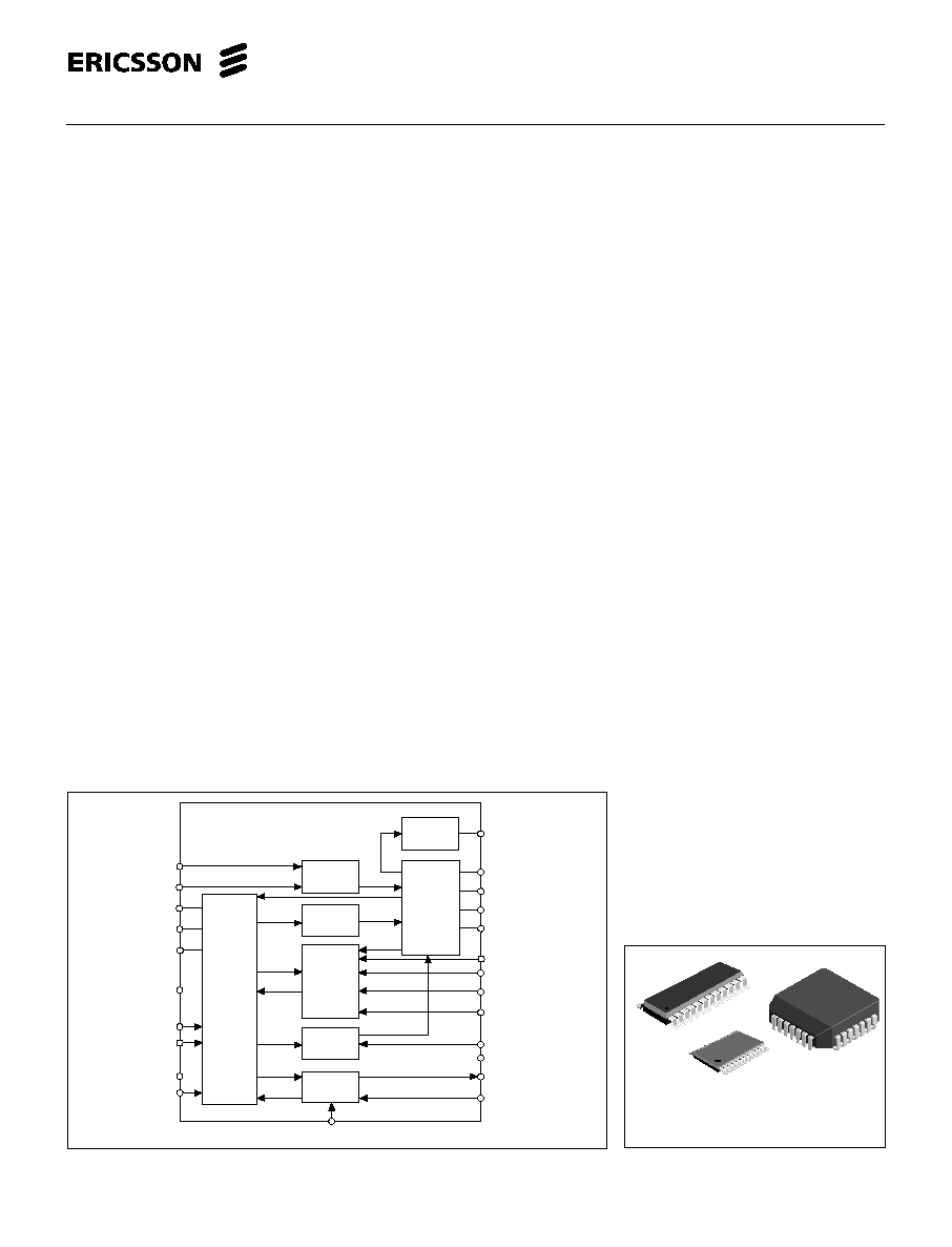
Figure 1. Block diagram.
June 1999
PBL 386 20/2
Subscriber Line
Interface Circuit
Key Features
∑ 24-pin SSOP package
∑ High and low battery with automatic
switching
∑ 60 mW on-hook power dissipation in
active state
∑ On-hook transmission
∑ Long loop battery feed tracks Vbat for
maximum line voltage
∑ Only +5 V feed in addition to battery
∑ Selectable transmit gain (1x or 0.5x)
∑ No power-up sequence
∑ 44V open loop voltage @ -48V battery
feed
∑ Full longitudinal current capability
during on-hook state
∑ Analog over temperature protection
permits transmission while the
protection circuit is active
∑ Integrated Ring Relay driver
∑ Ground key detector
∑ Programmable signal headroom
24-pinSOIC, 24-pin SSOP, 28-pin PLCC
RRLY
C1
C2
C3
DET
PSG
REF
LP
PLD
PLC
VTX
RSN
PTG
BGND
AGND
VBAT
VBAT2
VCC
HP
RINGX
TIPX
DR
DT
Ring Relay
Driver
Input
Decoder
and
Control
Ring Trip
Comparator
Ground Key
Detector
Line Feed
Controller
and
Longitudinal
Signal
Suppression
Off-hook
Detector
VF Signal
Transmission
Two-wire
Interface
POV
PBL
386 20/2
PBL 386 20/2
1
PBL 386 20/2

PBL 386 20/2
2
Maximum Ratings
Parameter
Symbol
Min
Max
Unit
Temperature, Humidity
Storage temperature range
T
Stg
-55
+150
∞
C
Operating temperature range
T
Amb
-40
+110
∞
C
Operating junction temperature range, Note 1
T
J
-40
+140
∞
C
Power supply, 0
∞
C
T
Amb
+70
∞
C
V
CC
with respect to A/BGND
V
CC
-0.4
6.5
V
V
Bat2
with respect to A/BGND
V
Bat2
V
Bat
0.4
V
V
Bat
with respect to A/BGND, continuous
V
Bat
-75
0.4
V
V
Bat
with respect to A/BGND, 10 ms
V
Bat
-80
0.4
V
Power dissipation
Continuous power dissipation at T
Amb
+70
∞
C
P
D
1.5
W
Ground
Voltage between AGND and BGND
V
G
-0.3
0.3
V
Relay Driver
Ring relay supply voltage
BGND+14 V
Ring trip comparator
Input voltage
V
DT
, V
DR
V
Bat
AGND
V
Input current
I
DT
, I
DR
-5
5
mA
Digital inputs, outputs (C1, C2, C3, DET)
Input voltage
V
ID
-0.4
V
CC
V
Output voltage
V
OD
-0.4
V
CC
V
TIPX and RINGX terminals, 0
∞
C < T
Amb
< 70
∞
C, V
Bat
= -50V
Maximum supplied TIPX or RINGX current
I
TIPX
, I
RINGX
-100
+100
mA
TIPX or RINGX voltage, continuous (referenced to AGND), Note 2
V
TA
, V
RA
-80
2
V
TIPX or RINGX, pulse < 10 ms, t
Rep
> 10 s, Note 2
V
TA
, V
RA
V
Bat
-10
5
V
TIPX or RINGX, pulse < 1
µ
s, t
Rep
> 10 s, Note 2
V
TA
, V
RA
V
Bat
-25
10
V
TIPX or RINGX, pulse < 250 ns, t
Rep
> 10 s, Notes 2 & 3
V
TA
, V
RA
V
Bat
-35
15
V
Recommended Operating Condition
Parameter
Symbol
Min
Max
Unit
Ambient temperature
T
Amb
0
+70
∞
C
V
CC
with respect to AGND
V
CC
4.75
5.25
V
V
Bat
with respect to AGND
V
Bat
-58
-8
V
AGND with respect to BGND
V
G
-100
100
mV
Notes
1. The circuit includes thermal protection. Operation at or above 140
∞
C junction temperature may degrade device reliability.
2. With the diodes D
VB
and D
VB2
included, see figure 12.
3. R
F1
and R
F2
20
is also required. Pulse is applied to TIP and RING outside R
F1
and R
F2
.
PBL 386 20/2
3
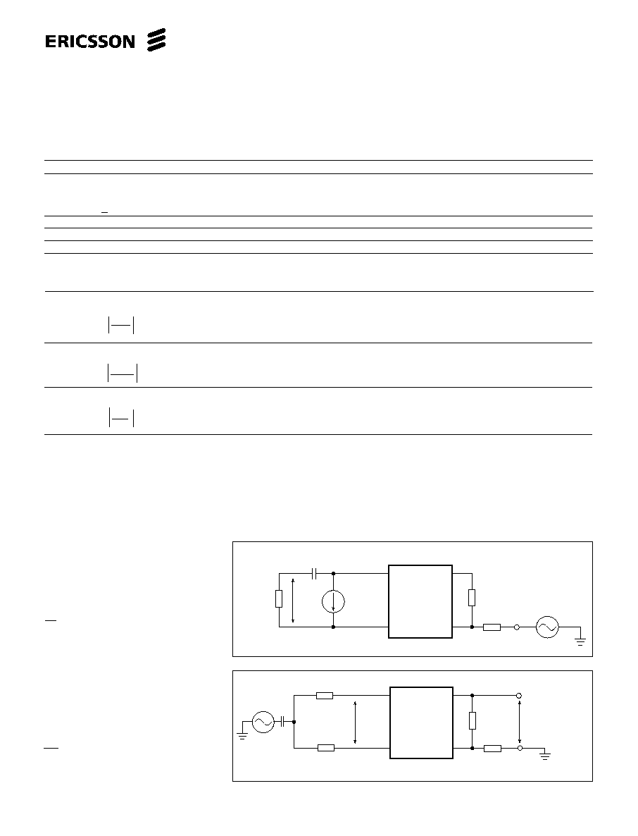
Figure 2. Overload level, V
TRO
, two-wire
port
1
<< R
L
, R
L
= 600
C
R
T
= 120 k
, R
RX
= 60 k
Electrical Characteristics
0
∞
C
T
Amb
+70
∞
C, PTG = open (see pin description), V
CC
= +5V
±
5 %, V
Bat
= -58V to -40V, V
BAT2
= -17V, R
LC
=38.3 k
, I
L
= 22 mA.
R
L
= 600
, R
F1
= R
F2
=R
P1
= R
P2
=0
, R
Ref
= 49.9 k
, C
HP
= 47 nF, C
LP
=0.15
µ
F, R
T
= 120 k
, R
SG
= 0 k
, R
RX
= 60 k
, R
R
= 52.3 k
,
R
OV
=
unless otherwise specified. Current definition: current is positive if flowing into a pin.
Ref
Parameter
fig
Conditions
Min
Typ
Max
Unit
Two-wire port
Overload level, V
TRO
2
Active state
1% THD, R
OV
=
1.0
V
Peak
On-Hook, I
Ldc
< 5mA
Note 1
1.0
V
Peak
Input impedance, Z
TR
Note 2
Z
T
/200
Longitudinal impedance, Z
LOT
, Z
LOR
0 < f < 100 Hz
20
35
/wire
Longitudinal current limit, I
LOT
, I
LOR
active state
10
mA
rms
/wire
Longitudinal to metallic balance, B
LM
IEEE standard 455-1984
0.2 kHz < f < 1.0 kHz
53
dB
1.0 kHz < f < 3.4 kHz
53
dB
Longitudinal to metallic balance, B
LME
3
0.2 kHz < f < 1.0 kHz
53
75
dB
B
LME
= 20 ∑ Log
E
Lo
1.0 kHz < f < 3.4 kHz
53
70
dB
V
TR
Longitudinal to four-wire balance, B
LFE
3
0.2 kHz < f < 1.0 kHz
53
75
dB
B
LFE
= 20 ∑ Log
E
Lo
1.0 kHz < f < 3.4 kHz
53
70
dB
V
TX
Metallic to longitudinal balance, B
MLE
4
0.2 kHz < f < 3.4 kHz
40
50
dB
V
TR
B
MLE
= 20 ∑ Log ; E
RX
= 0
V
Lo
PBL 386 20/2
TIPX
RINGX
RSN
VTX
R
T
R
RX
E
RX
R
L
V
TRO
I
LDC
C
PBL 386 20/2
TIPX
RINGX
RSN
VTX
R
T
R
RX
V
TX
R
LT
C
V
TR
R
LR
E
Lo
Figure 3. Longitudinal to metallic (B
LME
)
and Longitudinal to four-wire (B
LFE
) bal-
ance
1
<< 150
, R
LR
=R
LT
=R
L
/2=300
C
R
T
= 120 k
, R
RX
= 60 k
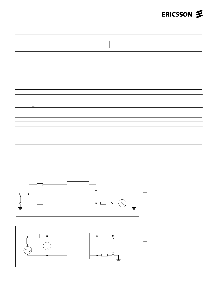
PBL 386 20/2
4
Parameter
fig
Conditions
Min
Typ
Max
Unit
Four-wire to longitudinal balance, B
FLE
4
0.2 kHz < f < 3.4 kHz
40
50
dB
E
RX
B
FLE
= 20 ∑ Log
V
Lo
Two-wire return loss, r
|Z
TR
+ Z
L
|
r = 20 ∑ Log
|Z
TR
- Z
L
|
0.2 kHz < f < 1.0 kHz
30
35
dB
1.0 kHz < f < 3.4 kHz, Note 3
20
22
dB
TIPX idle voltage, V
Ti
active, I
L
=0 mA
- 1.1
V
RINGX idle voltage, V
Ri
active, I
L
=0 mA
V
Bat
+2.5
V
V
TR
active, I
L
=0 mA
V
Bat
+3.6
V
Four-wire transmit port (VTX)
Overload level, V
TXO
5
Load impedance > 20 k
,
1.0
V
Peak
1% THD, Note 4
On-hook, I
L
< 5mA
1.0
V
Peak
Output offset voltage,
V
TX
-100
100
mV
Output impedance, z
TX
0.2 kHz < f < 3.4 kHz
15
50
Four-wire receive port (RSN)
Receive summing node (RSN) DC voltage
I
RSN
= -55
µ
A
1.15
1.25
1.35
V
Receive summing node (RSN) impedance
0.2 kHz < f < 3.4 kHz
8
20
Receive summing node (RSN)
0.3 kHz < f < 3.4 kHz
current (I
RSN
) to metallic loop current (I
L
)
200
ratio
gain,
RSN
Frequency response
Two-wire to four-wire, g
2-4
6
relative to 0 dBm V
rms
, 1.0 kHz. E
RX
= 0 V
0.3 kHz < f < 3.4 kHz
-0.20
0.10
dB
f = 8.0 kHz, 12 kHz, 16 kHz
-1.0
0.1
dB
Figure 4. Metallic to longitudinal and four-
wire to longitudinal balance
1
<< 150
, R
LT
= R
LR
= R
L
/2
=300
C
R
T
= 120 k
, R
RX
= 60 k
Figure 5. Overload level, V
TXO
, four-wire
transmit port
1
<< R
L
, R
L
= 600
C
R
T
= 120 k
, R
RX
= 60 k
Ref
PBL 386 20/2
TIPX
RINGX
RSN
VTX
R
T
R
RX
E
RX
R
LT
C
V
TR
R
LR
V
Lo
PBL 386 20/2
TIPX
RINGX
RSN
VTX
R
T
R
RX
R
L
I
LDC
C
E
L
V
TXO
PBL 386 20/2
5
Four-wire to two-wire, g
4-2
6
relative to 0 dBm, 1.0 kHz. E
L
=0 V
0.3 kHz < f < 3.4 kHz
-0.2
0.1
dB
f = 8 kHz, 12 kHz,
-1.0
0
dB
16 kHz
-2.0
0
dB
Four-wire to four-wire, g
4-4
6
relative to 0 dBm.1.0 kHz, E
L
=0 V
0.3 kHz < f < 3.4 kHz
-0.2
0.1
dB
Insertion loss
Two-wire to four-wire, G
2-4
6
0 dBm, 1.0 kHz, Note 5
V
TX
G
2-4
= 20 ∑ Log ; E
RX
= 0
-0.2
0.2
dB
V
TR
PTG = AGND
-6.22
-6.02
-5.82
dB
Four-wire to two-wire, G
4-2
6
0 dBm, 1.0 kHz, Note 6
V
TR
G
4-2
= 20 ∑ Log ; E
L
= 0
-0.2
0.2
dB
E
RX
Gain tracking
Two-wire to four-wire
6
Ref. -10 dBm, 1.0 kHz, Note 7
-40 dBm to + 0 dBm
-0.1
0.1
dB
-55 dBm to -40 dBm
-0.2
0.2
dB
Four-wire to two-wire
6
Ref. -10 dBm
-40 dBm to + 0 dBm
-0.1
0.1
dB
-55 dBm to -40 dBm
-0.2
0.2
dB
Noise
Idle channel noise at two-wire
C-message weighting
12
dBrnC
(TIPX-RINGX) or four-wire (VTX) output
Psophometrical weighting
-78
dBmp
Note 8
Harmonic distortion
Two-wire to four-wire
6
0 dBm
-67
-50
dB
Four-wire to two-wire
0.3 kHz < f < 3.4 kHz
-67
-50
dB
Battery feed characteristics
Constant loop current, I
LProg
12
I
LProg
= 1 000 - 4.0 (mA)
0.92 I
LProg
I
LProg
1.08 I
LProg
mA
R
LC
I
LProg
@ 30 mA
12
I
LProg
= 1 000 - 4.2 (mA)
0.95 I
LProg
I
LProg
1.05 I
LProg
mA
R
LC
I
LProg
@ 18 mA
12
I
LProg
= 1 000 - 3.9 (mA)
0.94 I
LProg
I
LProg
1.06 I
LProg
mA
R
LC
R
LC
in k
Open circuit state loop current, I
LOC
R
L
= 0
-100
0
100
µ
A
Ref
Parameter
fig
Conditions
Min
Typ
Max
Unit
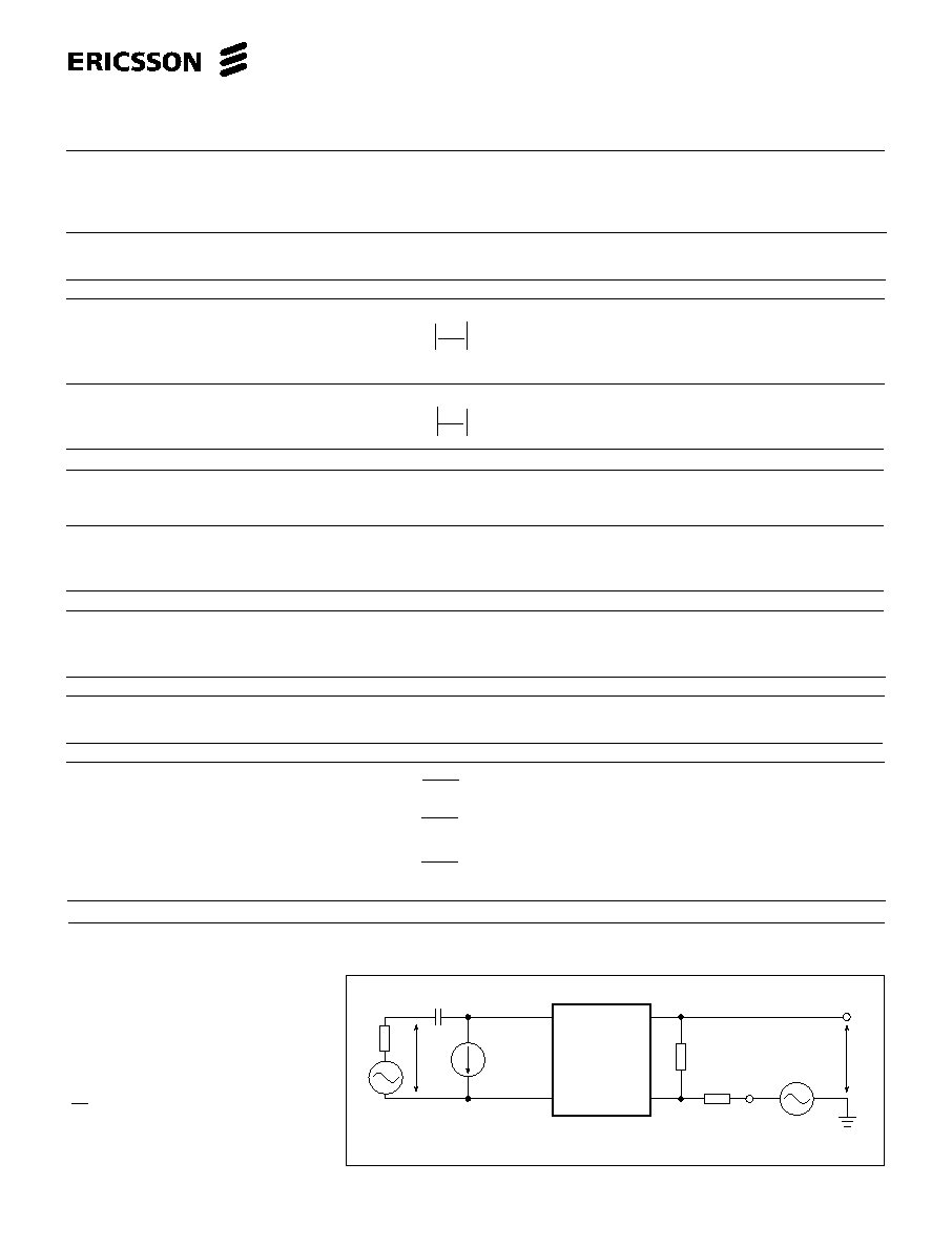
Figure 6.
Frequency response, insertion loss,
gain tracking.
1
<< R
L
, R
L
= 600
C
R
T
= 120 k
, R
RX
= 60 k
PBL 386 20/2
TIPX
RINGX
RSN
VTX
R
T
R
RX
E
RX
R
L
V
TR
I
LDC
C
E
L
V
TX