 | –≠–ª–µ–∫—Ç—Ä–æ–Ω–Ω—ã–π –∫–æ–º–ø–æ–Ω–µ–Ω—Ç: PBM3960QN | –°–∫–∞—á–∞—Ç—å:  PDF PDF  ZIP ZIP |
Description
PBM 3960/1 is a dual 7-bit+sign, Digital-to-Analog Converter (DAC) especially
developed to be used together with the PBL 3771/1, Precision Stepper Motor driver
in micro-stepping applications. The circuit has a set of input registers connected to an
8-bit data port for easy interfacing directly to a microprocessor. Two registers are
used to store the data for each seven-bit DAC, the eighth bit being a sign bit (sign/
magnitude coding). A second set of registers are used for automatic fast/slow current
decay control in conjunction with the PBL 3771/1, a feature that greatly improves
high-speed micro-stepping performance. The PBM 3960/1 is fabricated in a high-
speed CMOS process.
Key Features
∑
Analog control voltages from 3 V
down to 0.0 V.
∑
High-speed microprocessor interface.
∑
Automatic fast/slow current decay
control.
∑
Full-scale error
±
1 LSB.
∑
Interfaces directly with TTL levels and
CMOS devices.
∑
Fast conversion speed, 3
µ
s.
∑
Matches PBL 3771.
PBM 3960/1
Microstepping Controller/
Dual Digital-to-Analog Converter
February 1999
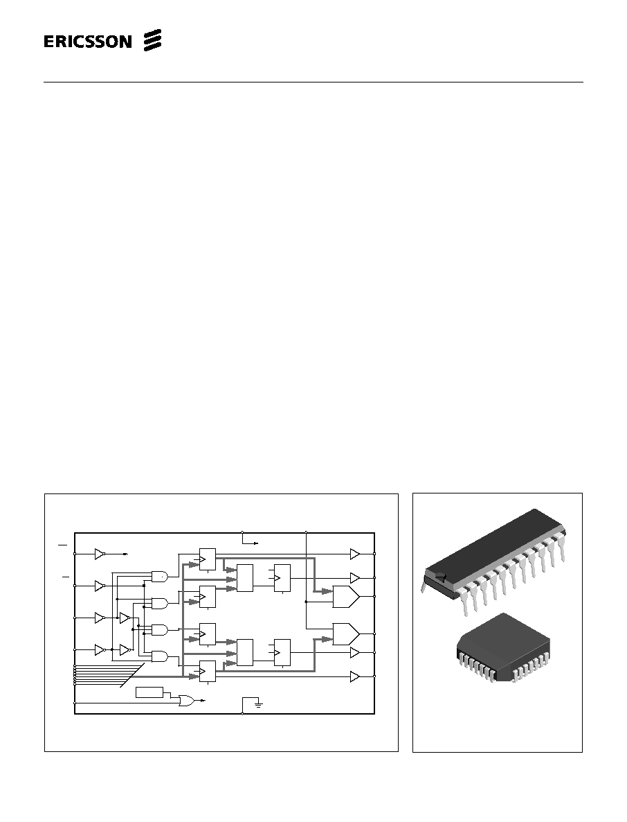
Figure 1. Block Diagram.
22-pin plastic DIP
28-pin plastic PLCC
V
DD
V
Ref
CS
A0
A1
WR
D7 - D0
RESET
V
ss
Sign 2
CD2
DA
2
Sign
1
CD
1
DA
1
E
C
D
R
E
C
D
E
C
D
R
R
E
C
D
R
Digit
Comp
Digit
Comp
E
C
D
R
E
C
D
R
D / A
D / A
E1
E2
E3
E4
POR
E1
E4
PBM 3960/1
DA- Data 1
DA- Data 2
Level 1
Level 2
R
PBM3960/1
PBM
3960/1

PBM 3960/1
2
Maximum Ratings
Parameter
Pin no. *
Symbol
Min
Max
Unit
Voltage
Supply
5
V
DD
6
V
Logic inputs
6- 17
V
I
-0.3
V
DD
+ 0.3
V
Reference input
1
V
R
-0.3
V
DD
+ 0.3
V
Current
Logic inputs
6- 17
I
I
-0.4
+0.4
mA
Temperature
Storage temperature
T
S
-55
+150
∞
C
Operating ambient temperature
T
J
-20
+85
∞
C
* refers to DIP package
Recommended Operating Conditions
Figure 2. Timing.
Figure 3. Timing of Reset.
t
t
t
t
t
t
t
CS
A0-A1
D0-D7
WR
DA
Sign, CD
cs
ch
as
ah
ds
dh
WR
t
DAC
t
pwr
t
t
Reset
Sign, CD
res
pres
Parameter
Symbol
Min
Typ
Max
Unit
Supply voltage
V
DD
4.75
5.0
5.25
V
Reference voltage
V
R
0
2.5
3.0
V

PBM 3960/1
3
Electrical Characteristics
Electrical characteristics over recommended operating conditions.
Ref.
Parameter
Symbol fig
Conditions
Min
Typ
Max
Unit
Logic Inputs
Reset logic HIGH input voltage
V
IHR
3.5
V
Reset logic LOW input voltage
V
ILR
0.1
V
Logic HIGH input voltage
V
IH
2.0
V
Logic LOW input voltage
V
IL
0.8
V
Reset input current
I
IR
V
SS
< V
IR
< V
DD
-0.01
1
mA
Input current, other inputs
I
I
V
SS
< V
I
< V
DD
-1
1
µ
A
Input capacitance
3
pF
Internal Timing Characteristics
Address setup time
t
as
2
Valid for A0, A1
60
ns
Data setup time
t
ds
2
Valid for D0 - D7
60
ns
Chip select setup time
t
cs
2
70
ns
Address hold time
t
ah
2
0
ns
Data hold time
t
dh
2
0
ns
Chip select hold time
t
ch
2
0
ns
Write cycle length
t
WR
2
50
ns
Reset cycle lenght
t
R
3
80
ns
Reference Input
Input resistance
R
Ref
6
9
k
Logic Outputs
Logic HIGH output current
I
OH
V
O
= 2.4 V
-13
-5
mA
Logic LOW output current
I
OL
V
O
= 0.4 V
1.7
5
mA
Write propagation delay
t
p
WR
2
From positive edge of WR.
30
100
ns
outputs valid, C
load
= 120 pF
Reset propagation delay
t
p
R
3
From positive edge of Reset to
60
150
ns
outputs valid, C
load
= 120 pF
DAC Outputs
Reset open, V
Ref
= 2.5 V
Nominal output voltage
V
DA
0
V
Ref
- 1LSB V
Resolution
7
Bits
Offset error
7
0.2
0.5
LSB
Gain error
7
0.1
0.5
LSB
Endpoint nonlinearity
7
0.2
0.5
LSB
Differential nonlinearity
5, 6
0.2
0.5
LSB
Load error
(V
DA
, unloaded - V
DA
, loaded)
0.1
0.5
LSB
R
load
= 2.5 k
, Code 127 to DAC
Power supply sensitivity
Code 127 to DAC
0.1
0.3
LSB
4.75 V < V
DD
< 5.25 V
Conversion speed
t
DAC
2
For a full-scale transition to
±
0.5 LSB
3
8
µ
s
of final value, R
load
= 2.5 kohm, C
load
= 50 pF.
PBM 3960/1
4
Figure 4. Pin configuration.
Pin Descriptions
Refer to figure 4.
DIP
PLCC
Symbol
Description
1
9
V
Ref
Voltage reference supply pin, 2.5 V nominal (3.0 V maximum)
2
10
DA
1
Digital-to-Analog 1, voltage output. Output between 0.0 V and V
R
- 1 LSB.
3
12
Sign
1
Sign 1, TTL/CMOS level. To be connected directly to PBL 3771 Phase input.
Databit D7 is transfered non inverted from PBM 3960/1/1 data input.
4
13
CD
1
Current Decay 1, TTL/CMOS level. The signal is automatically generated when
decay level is programmed. LOW level = fast current decay.
5
14
V
DD
Voltage Drain-Drain, logic supply voltage. Normally +5 V.
6
15
WR
Write, TTL/CMOS level, input for writing to internal registers.
Data is clocked into flip flops on positive edge.
7
16
D7
Data 7, TTL/CMOS level, input to set data bit 7 in data word.
8
17
D6
Data 6, TTL/CMOS level, input to set data bit 6 in data word.
9
19
D5
Data 5, TTL/CMOS level, input to set data bit 5 in data word.
10
20
D4
Data 4, TTL/CMOS level, input to set data bit 4 in data word.
11
21
D3
Data 3, TTL/CMOS level, input to set data bit 3 in data word.
12
23
D2
Data 2, TTL/CMOS level, input to set data bit 2 in data word.
13
24
D1
Data 1, TTL/CMOS level, input to set data bit 1 in data word.
14
25
D0
Data 0, TTL/CMOS level, input to set data bit 0 in data word.
15
27
A0
Address 0, TTL/CMOS level, input to select data transfer,
A0 selects between cannel 1 (A0 = LOW) and channel 2 (A0 = HIGH).
16
28
A1
Address 1, TTL/CMOS level, input to select data transfer. A1 selects between normal
D/A register programming (A1 = LOW) and decay level register programming (A1 = HIGH).
17
1
CS
Chip Select, TTL/CMOS level, input to select chip and activate data transfer
from data inputs. LOW level = chip is selected.
18
2
V
SS
Voltage Source-Source. Ground pin, 0 V reference for all signals and
measurements unless otherwise noted.
19
3
CD
2
Current Decay 2, TTL/CMOS level. The signal is automatically generated
when decay level is programmed. LOW level = fast current decay .
20
4
Sign
2
Sign 2. TTL/CMOS level. To be connected directly to PBL 3771 sign input.
Data bit D7 is transfered non-inverted from PBM 3960/1 data input.
21
6
DA
2
Digital-to-Analog 2, voltage output. Output between 0.0 V and V
ref
- 1 LSB.
22
7
Reset
Reset, digital input resetting internal registers.
HIGH level = Reset, V
Res
3.5 V = HIGH level. Pulled low internally.
5
Not Connected
8
Not Connected
11
Not Connected
18
Not Connected
22
Not Connected
26
Not Connected
1
2
3
4
5
6
7
8
9
10
11
22
21
20
19
18
17
16
15
14
13
12
ref
DA
1
1
V
Reset
CS
V
Sign
CD
SS
1
PBM
3960/1N
DD
WR
D7
D6
D5
D4
D3
D2
D1
D0
A1
A0
V
2
CD
2
Sign
DA
2
5
6
7
8
9
10
11
25
24
23
22
21
20
19
4
3
2
1
28
27
26
12
13
14
15
16
17
18
PBM
3960/1QN
ref
DA
1
1
V
V
Sign
CD
1
DD
WR
D7
D6
D5
D4
D3
Reset
CS
SS
D2
D1
D0
A1
A0
V
2
CD
2
Sign
DA
2
N/C
N/C
N/C
N/C
N/C
N/C

PBM 3960/1
5
Figure 6. Errors in D/A conversion.
Differential non-linearity of less than 1 bit,
output is monotonic.
Figure 5. Errors in D/A conversion.
Differential non-linearity of more than 1
bit, output is non-monotonic.
Figure 7. Errors in D/A conversion. Non-
linearity, gain and offset errors.
More
than 2
bits
Negative
difference
Output
Input
Less
than 2
bits
Positive
difference
Output
Input
Endpoint
non-linearity
Offset error
Actual
Gain
error
Output
Input
Full scale
Correct
Definition of Terms
Resolution
Resolution is defined as the reciprocal of
the number of discrete steps in the DAC
output. It is directly related to the
number of switches or bits within the
DAC. For example, PBM 3960/1 has 2
7
,
or 128, output levels and therefor has 7
bits resolution. Remember that this is
not equal to the number of microsteps
available.
Linearity Error
Linearity error is the maximum deviation
from a straight line passing through the
end points of the DAC transfer
characteristic. It is measured after
adjusting for zero and full scale.
Linearity error is a parameter intrinsic to
the device and cannot be externally
adjusted.
Power Supply Sensitivity
Power supply sensitivity is a measure of
the effect of power supply changes on
the DAC full-scale output.
Settling Time
Full-scale current settling time requires
zero-to-full-scale or full-scale-to-zero
output change. Settling time is the time
required from a code transition until the
DAC output reaches within
±
1
/
2
LSB of
the final output value.
Full-scale Error
Full-scale error is a measure of the
output error between an ideal DAC and
the actual device output.
different levels for initiation of fast
current decay can be selected.
The sign outputs generate the phase
shifts, i.e., they reverse the current
direction in the phase windings.
Data Bus Interface
PBM 3960/1 is designed to be compat-
ible with 8-bit microprocessors such as
the 6800, 6801, 6803, 6808, 6809, 8051,
8085, Z80 and other popular types and
their 16/32 bit counter parts in 8 bit data
mode. The data bus interface consists of
8 data bits, write signal, chip select, and
two address pins. All inputs are TTL-
compatible (except reset). The two
address pins control data transfer to the
four internal D-type registers. Data is
transferred according to figure 10 and on
the positive edge of the write signal.
Current Direction, Sign
1
& Sign
2
These bits are transferred from D
7
when
writing in the respective DA register. A
0
and A
1
must be set according to the data
transfer table in figure 10.
Current Decay, CD
1
& CD
2
CD
1
and CD
2
are two active low signals
(LOW = fast current decay). CD
1
is
active if the previous value of DA-Data1
is strictly larger than the new value of
DA-Data1 and the value of the level
register LEVEL1 (L
61
... L
41
) is strictly
larger than the new value of DA-Data1.
CD
1
is updated every time a new value
is loaded into DA-Data1. The logic
definition of CD
1
is:
CD
1
= NOT{[(D
6
... D
0
) < (Q
61
... Q
01
)]
AND[(D
6
...D
4
) < (L
61
... L
41
)]}
Differential Non-linearity
The difference between any two
consecutive codes in the transfer curve
from the theoretical 1LSB, is differential
non-linearity
Monotonic
If the output of a DAC increases for
increasing digital input code, then the
DAC is monotonic. A 7-bit DAC which is
monotonic to 7 bits simply means that
increasing digital input codes will
produce an increasing analog output.
PBM 3960/1 is monotonic to 7 bits.
Functional Description
Each DAC channel contains two
registers, a digital comparator, a flip flop,
and a D/A converter. A block diagram is
shown on the first page. One of the
registers stores the current level, below
which, fast current decay is initiated.
The status of the CD outputs determines
a fast or slow current decay to be used
in the driver.
The digital comparator compares
each new value with the previous one
and the value for the preset level for fast
current decay. If the new value is strictly
lower than both of the others, a fast
current decay condition exists. The flip
flop sets the CD output. The CD output
is updated each time a new value is
loaded into the D/A register. The fast
current decay signals are used by the
driver circuit, PBL 3771/1, to change the
current control scheme of the output
stages. This is to avoid motor current
dragging which occurs at high stepping
rates and during the negative current
slopes, as illustrated in figure 9. Eight