 | –≠–ª–µ–∫—Ç—Ä–æ–Ω–Ω—ã–π –∫–æ–º–ø–æ–Ω–µ–Ω—Ç: PKC4113PI | –°–∫–∞—á–∞—Ç—å:  PDF PDF  ZIP ZIP |
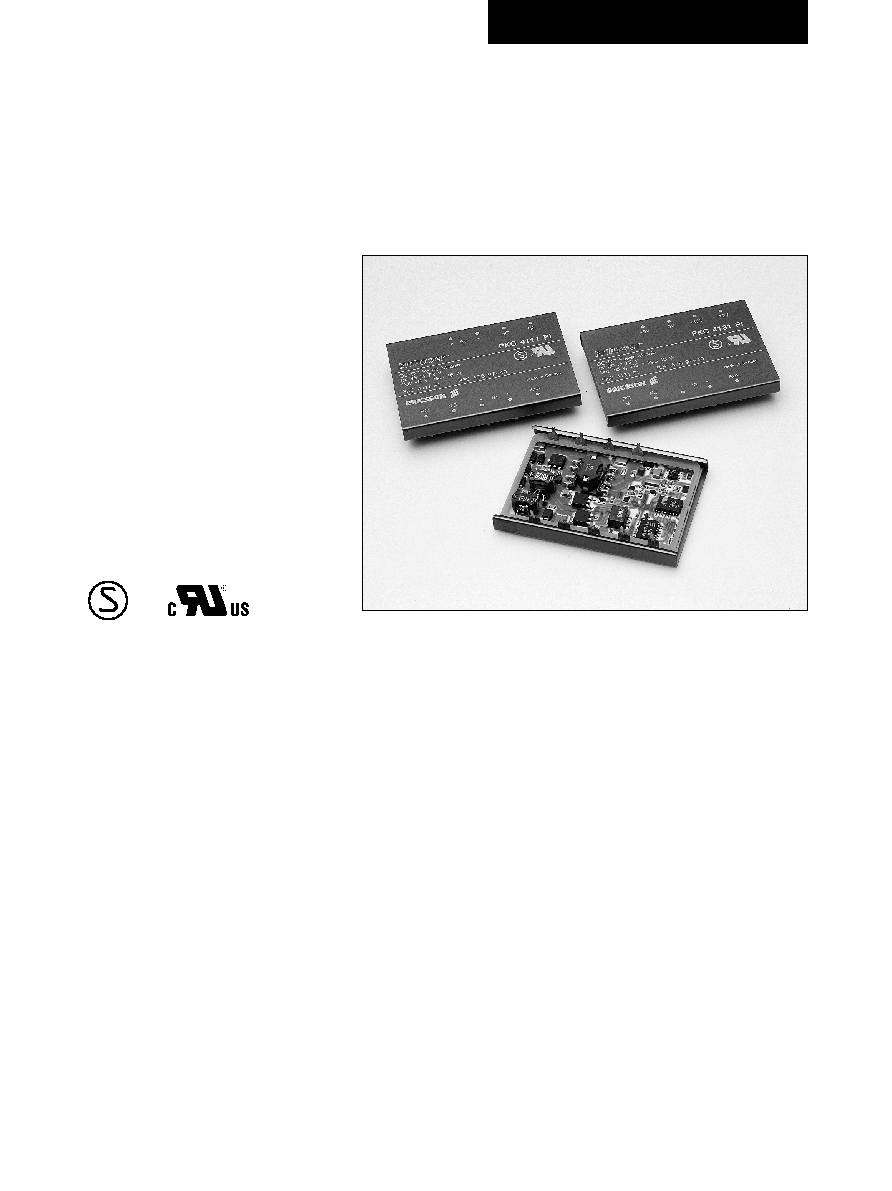
15≠18 W DC/DC Power Modules
48 V Input Series
∑ Regulated single, dual and
triple outputs
∑ Low profile 10.7 mm (0.42 in.),
allows 0.8 in. board pitch ≠ 0.6 in.
if recessed in the printed board
∑ Proven MTBF >2,000,000 hours
at +75 ∞C case temperature and a
rugged mechanical construction
∑ Efficiency 85% typ, at full load.
No extra heatsink up to +85∞C
ambient. Max. +115∞C case
∑ Low EMI in conformance with
class A in EN 55022 and
FCC part 15J
The 15≠18 watts PKC series DC/DC power modules
are especially designed for decentralized ≠48 and
≠60 Vdc systems with distributed on-board DC/DC
converters. Their low profile allows very narrow board
pitches and slim designs. By using thickfilm tech-
nology, which provides a high degree of integration as
well as efficient thermal management, and by
utilizing a 300 kHz switching frequency based on
proprietary drive & control circuits, these highly
reliable products can be used in demanding
Information Technology and Telecom (IT&T) applica-
tions e.g. computers, cellular radio, and telecom
switching. By using magnetic integration of the out-
put voltages in the feedback loop, all outputs are kept
within a ±3% total tolerance band. Input to output
E
isolation is 500 Vdc and mechanical ruggedness ≠
specified in conformance with IEC 68-2 ≠ is close to
requirements for discrete components. Extreme
temperature conditions can be met since the PKC
power modules can operate with full output power in
ambient temperatures from ≠45 to +85∞C, or up to
+115∞C case temperature also making the products
ideal for applications within not temperature con-
trolled environments.
The PKC series are manufactured using highly
automated manufacturing lines with a world-class
quality commitment and a five-year warranty.
Ericsson Microelectronics AB has been an ISO 9001
certified supplier since 1991. For a complete product
program please reference the back cover.
PKC 4000 I
2
EN/LZT 146 25 R1A (Replaces EN/LZT 137 06 R2) © Ericsson Microelectronics AB, June 2000
General
Stress in excess of Absolute Maximum Ratings may cause permanent damage. Absolute Maximum
Ratings, sometimes referred to as no destruction limits, are normally tested with one parameter at a
time exceeding the limits of Output data or Electrical Characteristics. If exposed to stress above these
limits, function and performance may degrade in an unspecified manner.
Safety
The PKC 4000 I Series DC/DC power
modules are designed in accordance with
EN
60 950, Safety of information technology
equipment including electrical business equip-
ment, and certified by SEMKO.
The PKC power modules are recognized
by UL and meet the applicable require-
ments in UL 1950 Safety of information
technology equipment, the applicable Canadi-
an safety requirements and UL 1012
Standard for power supplies.
The DC/DC power module shall be in-
stalled in an end-use equipment. Abnor-
mal/Component tests are conducted with
the DC/DC power module input protected
by an external 3 A fuse. The need for
repeting these tests in the end-use appli-
ance shall be considered if installed in a
circuit having higher rated devices.
When the supply to the DC/DC power
module meets all the requirements for
SELV (<60Vdc), the output is considered
to remain within SELV limits (level 3).
The isolation is an operational insulation
in accordance with EN 60 950.
The DC/DC power module is intended to
be supplied by isolated secondary circuitry
and shall be installed in compliance with
the requirements of the ultimate applica-
tion. If the products are connected to a
60 Vdc system reinforced insulation must
be provided in the power supply that
isolates the input from the ac mains. Sin-
gle fault testing in the power supply must
be performed in combination with the
DC/DC power module to demonstrate
that the output meets the requirement for
SELV. One pole of the input and one pole
of the output is to be grounded or both
are to be kept floating.
Considerations should be given to measur-
ing the case temperature to comply with
max T
Cnorm
when operated at normal
conditions in the end-use equipment.
The terminal pins are only intended for
connection to mating connectors of inter-
nal wiring inside the end-use equipment.
These DC/DC power modules may be used
in telephone equipment in accordance
with paragraph 34 A.1 of UL 1459
(Standard for Telephone Equipment, sec-
ond edition).
The isolation voltage between input and
output and between case and input/output
is 500 Vdc and the capacitor between
input and output has a value of 10 nF.
The leakage current is less than 1uA @
50 Vdc.
The case is designed in non-coductive
plastic. Its flammability ratings meets
UL 94V-0.
Notes:
1)
Corresponding ambient temp. range (T
A
) at full output power is ≠ 45 to +85 ∞C.
2)
P<0.6 kW, t
r
/t
d
= 10/1000 ms, I
I
< 8 A. Transient supressor threshold voltage is 76 V typ.
3)
The converters will operate down to V
I
£ 35V, when V
I
decreases, but will turn on at
V
I
£ 36 V, when V
I
increases (see also Operating information).
Absolute Maximum Ratings
T
C
Case temperature
1)
≠ 45
+115
∞C
W
tr
Transient input energy
2)
0.6
Ws
T
S
Storage temperature
≠ 55
+125
∞C
V
I
Input voltage
≠ 0.5
72
V dc
V
RC
Remote control voltage pin 1
0
5
V dc
V
ISO
Input to output isolation
500
V dc
Characteristics
min
max
Unit
Input T
C
< T
Cmax
unless otherwise specified
Characteristics
Conditions
min
typ
max
Unit
V
I
Input voltage range
3)
18
72
V
V
Ioff
Turn-off input voltage
(See Operating Information)
28
35
V
V
Ion
Turn-on input voltage
(See Operating Information)
29
36
V
C
I
Input capacitance
1.0
mF
V
I
= 53V, I
O
= 0,
Input stand-by power
T
C
= 0... +95 ∞C,
0.6
W
RC connected to pin 3
I
O
= 0, T
C
= 0...+95 ∞C
2
W
Equivalent inrush
current resistance
1
W
r
Irush
Input idling power
P
Ii
P
RC
Characteristics
Frequency
10...500 Hz
Amplitude
0.75 mm
Acceleration
10 g
Number of cycles
10 in each axis
Vibration
(Sinusoidal)
IEC 68-2-6 F
c
Test procedure & conditions
Environmental Characteristics
Temperature
85∞C
Humidity
85% RH
Duration
500 hours
Peak acceleration
200 g
Shock duration
3 ms
Peak acceleration
40 g
Bump duration
6 ms
Number of bumps
1000 in 6 directions
Temperature
≠40∞C...+125∞C
Number of cycles
10
Temperature
40∞C
Duration
56 days
Temperature,solder
260∞C
Duration
10...13 s
Shock
(Half sinus)
Bump
(Half sinus)
Temperature
change
Damp heat
Accelerated
damp heat
Solder
resistability
IEC 68-2-27 E
a
IEC 68-2-29 E
b
IEC 68-2-14 N
a
IEC 68-2-3 C
a
IEC 68-2-3 C
a
with bias
IEC 68-2-20 T
b
1A
3
EN/LZT 146 25 R1A (Replaces EN/LZT 137 06 R2) © Ericsson Microelectronics AB, June 2000
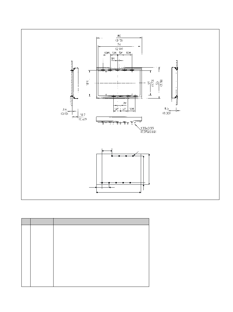
Mechanical Data
On-card mounting
In-card mounting
Footprint
Dimensions in mm (in)
Case
Blue anodized aluminum case with a
plastic bottom cover and with tin plated
brass pins.
Weight
50 gr (1.76 oz).
Pin spacing figures are nominal ±0.1M. 1M = 2.54 mm (0.1 in)
1
1
2
3
4
5
6
7
8
9
E
17.8
(0.70)
TOP VIEW
4.64
(0.183)
45.7
(1.80)
55
(2.16)
80 (3.15)
12.7
(0.50)
12.06
(0.475)
∆
¥
1.8-2.0 [9 ]
(0.079)
Pin
Designation
Function
Connections
1
RC
Remote Control to turn-on and turn-off the output. It is also used to
adjust the turn-off input voltage threshold (see V
Ioff
p.15)
2
NC
The pin is Not Connected
3
≠In
Negative Input terminal
4
+In
Positive Input terminal
5
Aux
Auxiliary terminal (see V
Ioff
p. 15)
6
Out
Negative Output terminal. Output 2 in dual and Output 3 in triple
output models
7
Out
Positive Output terminal. Output 2 in triple output models. Additional
return in dual versions
8
Rtn
Return terminal for all outputs
9
Out
Positive Output terminal. Output 1 in all models
4
EN/LZT 146 25 R1A (Replaces EN/LZT 137 06 R2) © Ericsson Microelectronics AB, June 2000
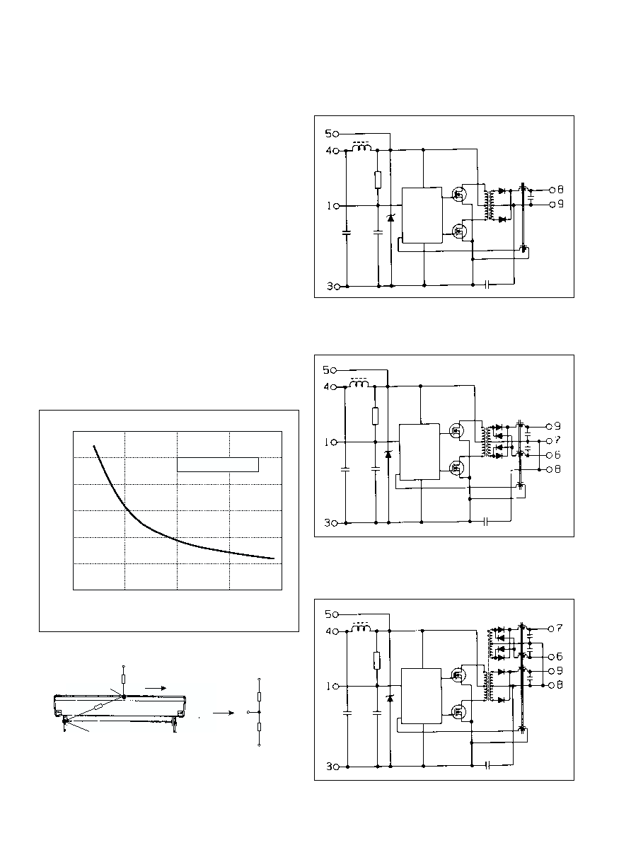
Thermal Data
Electrical Data
Single output
Fundamental circuit diagrams
Triple output
Dual output
T
sub
R
th sub-A
R
th sub-P
T
A
T
P
P
d
R
th sub-P
T
sub
R
th sub-A
v
T
A
T
P
5
10
15
0
0
0.5
1.0
2.0
1.5
Air velocity (m/s)
R
(
C/W)
th
sub-A
∞
R
= 6.0 C
th sub-P
∞
Two-parameter model
Power dissipation is generated in the components mounted on the
ceramic substrate. The thermal properties of the PKC power
module is determined by thermal conduction in the connected
pins and thermal convection from the substrate via the case.
The two-parameter model characterize the thermal properties of
the PKC power module and the equation below can be used for
thermal design purposes if detailed information is needed. The
values are given for a module mounted on a printed board assem-
bly (PBA).
Note that the thermal resistance between the substrate and the
air, R
th sub-A
is strongly dependent on the air velocity.
T
sub
= P
d
◊ R
th sub-P
◊ R
th sub-A
/(R
th sub-P
+ R
th sub-A
) + (T
P
≠T
A
)
◊ R
th sub-A
/(R
th sub-P
+ R
th sub-A
) + T
A
Where:
P
d
: dissipated power, calculated as P
O
◊ (1/
h
-1).
T
sub
: max average substrate temperature,
ª T
C
max
.
T
A
: ambient air temperature at the lower side of the power
module.
T
P
: average pin temperature or solder joint temperature.
R
th sub-P
: thermal resistance from T
sub
to the pins.
R
th sub-A
: thermal resistance from T
sub
to T
A
.
v
: velocity of ambient air.
Air velocity in free convection is 0.2≠ 0.3 m/s (40-60 lfm).
5
EN/LZT 146 25 R1A (Replaces EN/LZT 137 06 R2) © Ericsson Microelectronics AB, June 2000
0
3.0
A
PKC 4111 PI
Characteristics
Conditions
Output 1
min
typ
max
Unit
5.03
5.06
5.10
V
5.25
V
60
mV
150
mV
+250
mV
≠250
mV
T
C
= 0 ... +95∞C, V
I
= 36...72 V unless otherwise specified.
≠15
mV
≠1.2
mV/∞C
20
ms
30
ms
15
W
3.1
A
<0.5
A
80
mV
p-p
100
mV
p-p
35
mV
rms
50
dB
100
ms
4.90
5.23
V
1)
See also Power derating.
Output
Characteristics
Conditions
Unit
min
typ
max
Efficiency
h
Power dissipation
P
d
Miscellaneous
80.5
81.5
%
3.4
W
I
O
= I
Omax
I
O
= I
Omax
, V
I
= 53V
Output voltage initial
setting and accuracy
T
C
= +25∞C, I
O
= 3A, V
I
= 53 V
V
Oi
Output voltage
tolerance band
V
O
Idling circuit voltage
I
O
= 0 A
Load regulation
I
O
= 0.1...1.0 ◊ I
Omax
, V
I
= 53 V
t
tr
Load transient voltage
V
tr
I
O
= 0.1...1.0 ◊ I
Omax
, V
I
= 53 V
load step = 2.4A
Temperature coefficient
T
coeff
Ramp-up time
t
r
Start-up time
t
s
0.10.9...◊ V
O
From V
I
connection
to V
O
= 0.9 ◊ V
Oi
Output current
I
O
Max output power
1)
P
Omax
Current limiting
threshold
I
lim
T
C
<T
C max
Short curcuit current
I
sc
V
O
= 0.2...0.5V, T
A
=25∞C
Hick-up
Output ripple & noice
20 Hz...5 MHz
Supply voltage
rejection (ac)
SVR
f = 100 Hz sine wave, 1V
p-p
, V
I
= 53 V
(SVR = 20 log (1 V
p-p
/V
Op-p
))
Line regulation
I
O
= I
Omax
Load transient
recovery time
I
O
= I
Omax
, T
C
<T
C max
V
Oac
I
O
=I
Omax
DC...50 MHz
1 MHz bandwidth
I
O
= 0.1...1.0 ◊ I
Omax
and long term drift
I
O
=
0.1...1.0 ◊ I
Omax
,
V
I
= 53 V
t = 0...10 minutes
Short term drift
di
dt
<1A/
ms