17- 30W DC/DC power modules
48V Input series
∑ Efficiency typ 90% from 30% to
full load for 3.3V converter
∑ Output current up to 14A
∑ Meets lead-free soldering
processes up to 260∞C
∑ Low profile 7.5 mm (0.295 in.)
∑ 1500 Vdc isolation voltage
∑ MTBF >5,100,000 hours at +75∞C
case temperature
∑ Full power up to +70∞C ambient at
1 m/s airflow
∑ Complete, no extra heatsinks
required
The PKD 4000 SI series of DC/DC power modules
are intended to be used as distributed power sources
in decentralized 48/60VDC power systems. The PKD
series use a ceramic substrate with thickfi lm tech-
nology and a high degree of silicon in te gra tion. That,
together with the electrical design using synchronous
rectifi cation gives good thermal management, high
reliability and high effi ciency.
The high effi ciency makes it possible to operate over a
wide temperature range without a heatsink. At forced
convection cooling >200lfm (1m/s), the PKD units
E
PKD 4000 SI
can deliver full power up to +70∞C ambient tem per a-
ture. The high reliability and the low profi le of the
PKD series makes them particularly suited for In for -
ma tion Technology and Telecom (IT&T) applications
with board spacing down to 15mm (0.6 in.).
These products are manufactured using highly au to -
mat ed manufacturing lines with a world-class quality
commitment and a fi ve-year warranty.
Ericsson Power Modules AB is an ISO 9001/14001
certifi ed supplier.
2
EN/LZT 146 120 R2B © Ericsson Power Modules AB, March 2003
Characteristics
Conditions
min
typ
max
Unit
V
I
Input voltage range
1)
36
75
V
V
Ioff
Turn-off input voltage
(See operating information)
32
V
V
Ion
Turn-on input voltage
See operating information)
36
V
C
I
Input Capacitance
1.4
µF
P
Ii
Input idling power
I
O
= 0, V
I
= 53 V
2.0
W
P
Ist-by
Input stand-by power
1)
V
I
= 53 V
0.5
W
Environmental Characteristics
General
Input T
C
< T
C max
Note:
1) The input voltage range 36...75 V meets
the requirements in the European Telecom
Standard prETS 300 132-2 for Normal input
voltage range in 48 V and 60 V DC power
systems, ≠40.5...≠57.0 V and ≠50.0...≠72.0
V respectively.
Safety
The PKD 4000 SI Series DC/DC converters
are designed in accordance with Safety stan-
dards IEC/EN/UL 60 950, Safety of Information
Technology Equipment.
The PKD 4000 SI Series DC/DC converters
are UL 60950 recognized and certifi ed in ac-
cordance with EN 60 950.
The DC/DC converter should be installed in
the end-use equipment in accordance with the
requirements of the ultimate equipment. The
input source must be isolated by minimum
Basic Insulation from the primary circuit in
accordance with IEC/EN/UL 60950.
If the input voltage to the DC/DC converter
is 75 V dc or less, then the output remains
SELV (Safety Extra Low Voltage) under nor-
mal and abnormal conditions.
Single fault testing in the input power source
circuit should be performed with the DC/DC
converter connected to demonstrate that the
input voltage does not exceed 75 V dc. If the
input power source circuit is a DC power sys-
tem, the source may be treated as a TNV2 cir-
cuit and testing has demonstrated compliance
with SELV limits and isolation requirements
equivalent to Basic Insulation in accordance
with IEC/EN/UL 60 950.
It is recommended that a fast blow fuse with
a rating of 2.5 A be used at the input of
each DC/DC converter. The PKD 4000 SI
series DC/DC converters are approved for a
maximum fuse rating of 15 A. If a fault occurs
in the DC/DC converter that imposes a short
circuit on the input power source, this fuse
will provide the following functions
- Isolate the faulty DC/DC converter from
the input power source not to affect the
operation of other parts of the system.
- Protect the distribution wiring from
excessive current and power loss thus
preventing hazardous overheating
The galvanic isolation is verifi ed in an electric
strength test. The test voltage (V
ISO
) between
input and output is 1,500 V dc for 60 s.
Leakage current is less than 1 µA at nominal
input voltage.
The fl ammability rating for all construc-
tion parts of the DC/DC converter meets UL
94V-0.
1)
With module inhibited with RC pin no 5.
Absolute Maximum Ratings
Stress in excess of Absolute Maximum Ratings may cause permanent damage. Absolute
Maximum Ratings, sometimes referred to as no destruction limits, are normally tested with one
parameter at a time exceeding the limits of Output data or Electrical Characteristics. If exposed
to stress above these limits, function and performance may degrade in an unspecifi ed manner.
1)
Measured on pin 22.
2)
V
OI
= initial output voltage setting.
Characteristics
min
max
Unit
T
C
Case temperature at max output power
1)
-45
+100
∫C
T
S
Storage temperature
-55
+125
∫C
V
I
Input voltage
-0.5
+80
Vdc
V
ISO
Isolation voltage
(Input to output test voltage)
1500
Vdc
V
RO
Remote on/off voltage pin 5
SI version
SIN version
-0.5
-0.5
+6
+9
Vdc
V
adj
Output adjust voltage pin 16
2)
-0.5
2xVoi
Vdc
Characteristics
Test procedure & conditions
Random vibration
IEC 68-2-34 Ed
Frequency
Spectral density
Duration
10 ... 500 Hz
0.025 g
2
/Hz
15 min each direction
Bump
IEC 68-2-29 Test Eb
Peak acceleration
Duration
Directions
number of bumps
40 g
6 ms
6
1000/direction
Shock
(Half sinus)
IEC 68-2-27
Peak acceleration
Shock duration
200 g
0.5 ms
Temperature change
JESD 22-A104
(IEC 68-2-14 N
a
)
Temperature
Number of cycles
-40 ... +125 ∫C
300
Operational Lifetime
test
Case temperature
Load
Input voltage
Duration
100 ∫C
Nominal
Max
1000 h
Accelerated damp
heat
IEC 68-2-3 Ca
with bias.
Nominal input voltage
Temperature
Humidity
Duration
85 ∫C
85 % RH
1000 hours
Resistance to
cleaning solvents
IEC 68-2-45 XA
Method 1
Water
Isopropyl alcohol
Glycol ether
Method
+55 ±5 ∫C
+35 ±5 ∫C
+35 ±5 ∫C
with rubbing
Moisture /
Reflow sensitivity
classification
IPC/JEDEC
J-STD-020A
Level 1
High Temperature Reflow
(See page 17)
3
EN/LZT 146 120 R2B © Ericsson Power Modules AB, March 2003
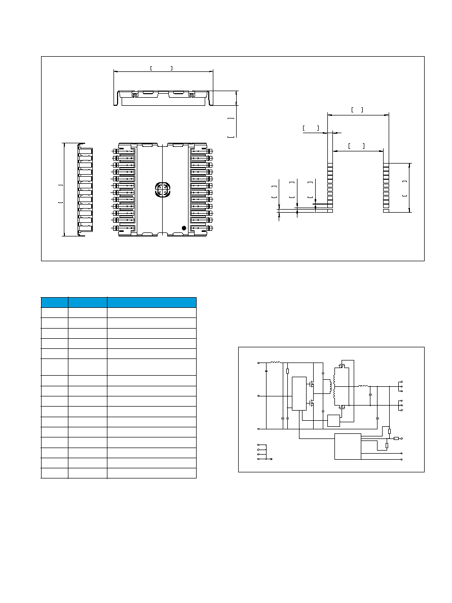
Pin
Designation
Function
1
Case
Case connection.
1)
2
+In
Positive input
3
-In
Negative input
4
NC
Not connected
5
RC
Remote control pin
6
RCS
For SI versions - Do not connect
For SIN versions - Connect to -In
7-11
NC
Not connected
12
Case
Case connection.
1)
13
Case
Case connection.
1)
14
NC
Not connected
15
+Sen
Positive remote sense
16
Vadj
Output voltage adjust
17
-Sen
Negative remote sense
18-20
-Out
Negative output
21-23
+Out
Positive output
24
Case
Case connection.
1)
Weight
Maximum: 22g.
Case
The cover is a part of the leadframe and functions as the
pick and place surface, shielding and additional heatsinking.
Connections
Fundamental circuit diagram
Single output
Electrical Data
Mechanical Data
1)
Case is floating and may be connected either to +V
In
;
-V
In
; +V
out
; -V
out
to optimize EMI performance.
21
22
23
18
19
20
16
2
5
3
Isolated
feedback
Control
Control
17
15
1
12
13
24
Case connection
Dimensions in mm [inch]
Coplanarity within 0.1 mm
Soldering pattern
4,4
0,173
42
1,654
40,8
1.606
50,8
2,0
2,8(24x)
0,1
1,2(2x)
0,047
0,6(20x)
0,024
FOOTPRINT
max 50,4
max 1.984
7,5
+0,5
-0,6
0,295
+0,02
-0,02
24
13
12
1
46,3
`0,3
1,822
`0,012

4
EN/LZT 146 120 R2B © Ericsson Power Modules AB, March 2003
PKD 4118 SIOD
T
C
= ≠25...+90∞C, V
I
= 36 ...75V unless otherwise specified.
Miscellaneous
Output
1) See Operating information.
2) See also Typical Characteristics, Power derating.
Characteristics
Conditions
min
typ
max
Unit
Efficiency
I
O
= I
Omax
, V
I
= 53 V, T
C
= +25∞C
82
85
%
P
d
Power dissipation
I
O
= I
Omax
, V
I
= 53 V, T
C
= +25∞C
3.2
W
fs
Switching frequency
145
150
165
kHz
Characteristics
Conditions
Output 1
Unit
min
typ
max
V
Oi
Output voltage initial
setting and accuracy
T
C
= +25∞C, I
O
= I
Omax
, V
I
= 53 V
1.19
1.20
1.21
V
Output adjust range
1)
1.08
1.32
V
O
Output voltage
tolerance band
Long term drift
included
I
O
=0.1 ...1.0
◊ I
O max
1.15
1.25
V
Idling voltage
I
O
= 0
1.15
1.25
Line regulation
I
O
=I
Omax
5
mV
Load regulation
I
O
=0.01 ...1.0
◊ I
O max
, V
I
= 53 V
5
mV
t
tr
Load transient recovery time
I
O
=0.1 ... 1.0
◊ I
O max
, V
I
= 53 V
load step = 0.5◊ I
Omax
100
µ
s
V
tr
Load transient voltage
I
O
=0.1 ... 1.0
◊ I
O max
, V
I
= 53 V
load step = 0.5◊ I
Omax
dI / dt = 5A / µs
±350
mV
T
coeff
Temperature coefficient
I
O
=I
O max
, T
C
<T
C max
0
±0.011
±0.25
mV/∫C
t
r
Ramp-up time
I
O
= 0.1...1.0
◊ I
O max
V
I
=53V
0.1 ...0.9
◊ V
O
20
ms
t
s
Start-up time
From V
I
connection
to V
O
= 0.9
◊ V
Oi
25
I
O
Output current
0
14
A
P
O max
Max output power
2)
Calculated value
16.8
W
I
lim
Current limiting threshold
T
C
< T
C max
16.5
A
I
sc
Short circuit current
T
C
= + 25∞C
20
A
V
O ac
Output ripple & noise
I
O
=I
O max
20 Hz ...5 MHz
30
60
mV
p-p
SVR
Supply Voltage Rejection (ac)
f = 100 Hz sine wave, 1 V
p-p
, V
I
= 53 V
(SVR = 20 log (1 V
p-p
/V
Op-p
))
70
dB