
DC/DC power module
1.8 V / 5A / 9W
The MacroDensTM PKF 4918B I true component level
on-board DC/DC power modules are intended
as distributed power sources in decentralized ≠ 48 and
≠60VDC power systems.
The over-moulded rugged design also makes them
suitable for other demanding industrial applications.
They are optimized for an operational ambient
∑ SMD package with ultra low
component height 8.0 mm (0.315 in.)
∑ 80% efficiency at full load
∑ 1,500 Vdc isolation voltage
∑ Synchronous rectification
∑ MTTF >10 million hours at +50∞C
case temperature (+40∞C ambient)
∑ Low EMI
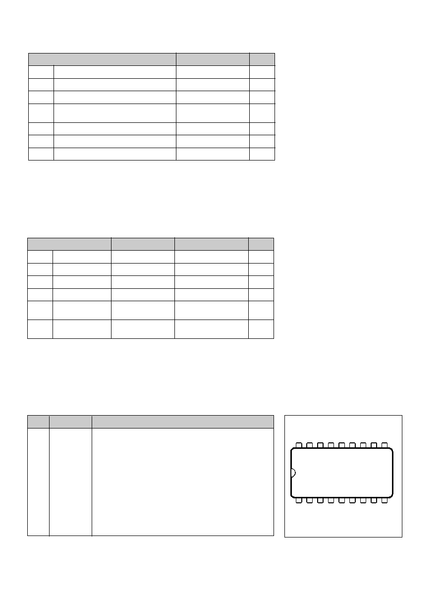
PKF 4918 B I
E
temperature range in compliance with present and
future application needs, including non temperature
controlled environments. The mechanical design
offers a surface mount version, delivered in
ready-to-use tubes, trays or tape & reel package, and
compatibility with semi and fully aqueous cleaning
processes.
Patents Pending
2
EN/LZT 146 63 R1A © Ericsson Microelectronics AB, March 2001
Stress in excess of Absolute Maximum
Ratings may cause permanent damage.
Absolute Maximum Ratings, sometimes
referred to as no destruction limits, are nor-
mally tested with one parameter at a
time exceeding the limits of Output data
or Electrical Characteristics. If exposed to
stress above these limits, function and per-
formance may degrade in an unspecified
manner.
Connections
* Output pin 3 is preferred, for optimum performance use both pin 1 & 3.
Absolute Maximum Ratings
Characteristics
Isolation voltage
(input to output test voltage)
V
ISO
min
max
Unit
T
C
Case temperature at full output power
≠45
+100
∞C
T
S
Storage temperature
≠55
+125
∞C
V
I
Continuous input voltage
1)
≠0.5
+75
V dc
1,500
V dc
V
tr
Transient input energy
0.10
Ws
V
RC
Remote control voltage pin 11 ref. to pin 17
≠5
+16
V dc
V
adj
Output adjust voltage pin 8 ref. to pin 17
≠5
+40
V dc
NOTES:
1)
The input voltage range 36...75 V dc meets
the European Telecom Standard prETS
300 132-2 Nominal input voltage range in
48 V and 60 V dc power systems,
≠ 40.5... ≠57.0 V and ≠50.0... ≠ 72.0 V
respectively. Absolute max continuous input
voltage is 75 V dc.
2)
The power modules will operate down to
£
35V, when V
I
decreases, but will turn on at
V
I
£
36V, when V
I
increases (see also Operating
information).
Input T
C
<T
Cmax
unless otherwise specified
mW
mW
Input stand-by power
P
RC
V
I
Input voltage range
1)2)
36
75
V
V
Ioff
Turn-off input voltage
30.0
35.0
V
33.5
See typical characteristics
V
Ion
Turn-on input voltage
36.0
V
34.5
See typical characteristics
C
I
Input capacitance
mF
1.4
P
Ii
Input idling power
I
O
= 0, T
C
= ≠30...+ 95 ∞C
(V
I
= 53V)
(V
I
= 66V)
1000
1200
(V
I
= 53V)
(V
I
= 66V)
41
66
T
C
= ≠30...+ 95 ∞C,
RC connected to pin 17
Characteristics
Conditions
min
typ
max
Unit
32.0
Pin
Designation
Function
1
Out 1
Output 1*
2
Rtn
Output return.
3
Out 1
Output 1, Preferred output *. Positive voltage ref. to Rtn.
4-7
NC
Not connected. Isolated from each other.
8
V
adj
Output voltage adjust.
9
NC
Not connected.
10
NC
Not connected.
11
RC
Remote control. Used to turn-on and turn-off output.
12≠16
NC
Not connected. Isolated from each other.
17
≠In
Negative input.
18
+In
Positive input.
18 17 16 15 14 13 12 11 10
1
2
3
4
5
6
7
8
9

3
EN/LZT 146 63 R1A © Ericsson Microelectronics AB, March 2001
Fundamental circuit diagram
Single output
Electrical Data
Safety
The PKF 4918 BI DC/DC power module is designed in accordance
with EN 60 950, Safety of information technology equipment including
electrical business equipment.
The PKF power modules are recognized by UL and meet the applica-
ble requirements in UL 1950 Safety of information technology equipment,
the applicable Canadian safety requirements and UL 1012 Standard for
power supplies.
The DC/DC power module shall be installed in an end-use equipment
and considerations should be given to measuring the case temperature
to comply with T
Cmax
when in operation. Abnormal component tests
are conducted with the input protected by an external
15 A fuse. The need for repeating these tests in the end-use
appliance shall be considered if installed in a circuit having higher
rated devices.
When the supply to the DC/DC power module meets all the require-
ments for SELV (<60Vdc), the output is considered to remain within
SELV limits (level 3). The isolation is an operational insulation in
accordance with EN 60 950.
The DC/DC power module is intended to be supplied by isolated
secondary circuitry and shall be installed in compliance with the re-
quirements of the ultimate application. If they are connected to a
60 V DC system reinforced insulation must be provided in the power
supply that isolates the input from the mains. Single fault testing in
the power supply must be performed in combination with the
DC/DC power module to demonstrate that the output meets the re-
quirement for SELV. One pole of the input and one pole of the output
is to be grounded or both are to be kept floating.
The terminal pins are only intended for connection to mating connec-
tors of internal wiring inside the end-use equipment.
These DC/DC power modules may be used in telephone equipment in
accordance with paragraph 34 A.1 of UL 1459 (Standard for Telephone
Equipment, second edition).
The galvanic isolation is verified in an electric strength test. Test
voltage (V
ISO
) between input and output is 1,500 Vdc for 60 s. In
production the test duration may be decreased to 1 s.
The capacitor between input and output has a value of 2,2 nF and the
leakage current is less than 1µA @ 53 Vdc.
The case is designed in non-conductive epoxy. Its flammability
rating meets UL 94V-0. The oxygen index is 34%.
Transient input voltage
Single voltage pulse at +25∞C ambient temperature.
4
EN/LZT 146 63 R1A © Ericsson Microelectronics AB, March 2001
T
C
= ≠30...+95 ∞C, V
I
= 36 ...75 V.
0
5
A
Characteristics
Conditions
Output 1
min
typ
max
Unit
Output voltage initial
setting and accuracy
V
Oi
Output voltage
tolerance band
V
O
Idling voltage
I
O
= 0 A
Load regulation
I
O
= 0...5 A, V
I
= 53 V
t
tr
Load transient voltage
V
tr
Temperature coefficient
2)
T
coeff
t
r
Start-up time
t
s
I
O
Max output power
2)
P
Omax
Current limiting
threshold
I
lim
T
C
<T
Cmax
, V
O
= 1.4 V
Short circuit current
I
sc
V
O
= 0.2...0.5V, T
C
= +25∞C
20 Hz...5 MHz
Line regulation
I
O
= 5 A
Load transient
recovery time
1.77
1.80
1.84
V
1.69
1.81
1.91
V
10
+300
mV
≠300
mV
+0.3
mV/∞C
2
ms
5
ms
9
W
5.5
6
A
7
A
50
mV
p-p
150
µs
1.71
1.89
V
Long term drift
included
Output
V
I
= 36...55 V
Output adjust range
1)
1.50
1.80
2.20
V
I
O
= 0.5...5 A, V
I
= 53 V
load step = 2.5 A
50
dB
1)
See also Operating Information
2)
See Typical Characteristics
T
C
= +25∞C, I
O
= 3.5 A, V
I
= 53 V
Ramp-up time
Output current
2)
I
O
= 3 A
Output ripple & noise
V
Oac
f = 100 Hz sine wave, 1V
p-p
, V
I
= 53 V
(SVR = 20 log (1 V
p-p
/V
Op-p
))
I
O
= 0.5...5 A
,
V
I
= 53 V
From V
I
connection to V
O
= 0.9 ◊V
Oi
I
O
=
0.3-5 A,
0.1...0.9 ◊V
O
, V
I
= 53 V
I
O
= 5 A, T
C
= +40...+90 ∫C
SVR
Supply voltage rejection (ac)
2.3
3.0
Characteristics
Conditions
Unit
min
typ
max
P
d
Power dissipation
Miscellaneous
%
Efficiency
I
O
= 5 A
75
80
V
I
= 53 V
V
I
= 66 V
V
I
= 53 V
V
I
= 66 V
75
79
2.4
3.0
W
V
I
= 55...75 V
≠2.5
mV
Calculated value
25
mV
I
O
= 0.5...5 A
I
O
= 0.5...3 A Pin 1
1.60
1.89
V
75
mV
p-p
0.4...50 MHz
I
O
= 5 A
20 Hz...5 MHz
80
dBµV

5
EN/LZT 146 63 R1A © Ericsson Microelectronics AB, March 2001
Typical Characteristics
Temperature coefficient
Turn-on/turn-off input voltage
Dynamic load response (typ) @ +25∞C
0.1 ms/div
The output voltage
deviation is deter-
mined by the load
transient (dI/dt)
Load change:
dI/dt 4 A/µs
2 A/div
200 mV/div
Current derating
Output characteristic (typ)
Power derating
Efficiency (typ)
@ T
A
= +25∞C
4.75
4.80
4.85
4.90
4.95
5.00
5.05
1.5
1.8
Output voltage (V) initial setting
Load curr
ent (A)
2.2
1.81
1.80
1.76
1.77
1.78
1.79
1.82
-30
-15
-0
+15
+30
+45
+60
+75 +90
0
1
2
3
4
5
6
7
1,74
1,76
1,78
1,80
1,82
1,84
1,86
Output voltage (V)
Load current (A)