 | –≠–ª–µ–∫—Ç—Ä–æ–Ω–Ω—ã–π –∫–æ–º–ø–æ–Ω–µ–Ω—Ç: PKF5617 | –°–∫–∞—á–∞—Ç—å:  PDF PDF  ZIP ZIP |

5≠6 W DC/DC Power Modules
Wide Input Series
∑ SMD and through-hole versions with
ultra low component height 8 mm
(0.315 in.)
∑ 18≠72 V input voltage range
∑ 82% efficiency (typ at 5 V)
∑ 1,500 V dc isolation voltage
∑ Switching frequency syncronization
∑ MTBF > 4.9 million hours at +55∞C
case temperature (+40 ∞C ambient)
∑ Low EMI measured according to
CISPR 22 and FCC part 15J
The MacroDensTM PKF 5000 I series true component
level on-board DC/DC power modules are intended
as distributed power sources in decentralized 24, 48
and 60 V DC power systems. Utilization of thick film
technology and a high degree of silicon integration
has made it possible to achieve a MTBF of more than
4.9 million hour.
The highly reliable and rugged over-moulded design
and the ultra low height of these DC/DC power
modules makes them particularly suited for Informa-
tion Technology and Telecom (IT&T) and other
demanding industrial applications, with board
spacing down to 15 mm or 0.6 in. These DC/DC
power modules are optimized for free convection
cooling and have an operational ambient temperature
range in compliance with present and future
application needs, including non temperature con-
trolled environments.
The mechanical design offers the choice of surface
mount or through-hole versions, delivered in ready-
to-use tubes, trays or tape & reel package, and
compatibility with semi and fully aqueous cleaning
processes.
The PKF series is manufactured using highly
automated manufacturing lines with a world-class
quality commitment and a five-year warranty.
Ericsson Microelectronics AB has been an ISO 9001
certified supplier since 1991. For a complete product
program please reference the back cover.
Patents
US: D357901 DE: M94022763
E
PKF 5000 I
2
EN/LZT 146 32 R1A (Replaces EN/LZT 137 27 R3) © Ericsson Microelectronics, June 2000
General
1)
The input voltage range 18...72 V dc meets
the European Telecom Standard
ETS 300 132-2 Nominal input voltage range
in 48 V and 60 V dc power systems, ≠ 40.5...
≠57.0 V and ≠50.0... ≠ 72.0 V respectively. At
input voltages exceeding 72 V (abnormal
voltage) the power loss will be higher than at
normal input voltage and T
C
must be limited to
max +90 ∞C. Absolute max continuous input
voltage is 75 V dc. Output characteristics will
be marginally affected at input voltages
exceeding 72 V.
2)
The test is applicable for through-hole
versions.
Stress in excess of Absolute Maximum Rat-
ings may cause permanent damage. Absolute
Maximum Ratings, sometimes referred to as
no destruction limits, are normally tested
with one parameter at a time exceeding the
limits of Output data or Electrical Charac-
teristics. If exposed to stress above these
limits, function and performance may de-
grade in an unspecified manner.
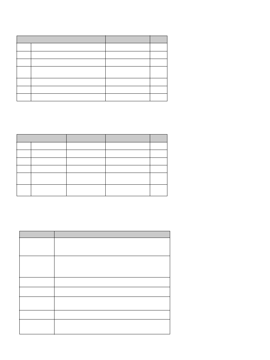
Absolute Maximum Ratings
Characteristics
Unit
Isolation voltage
(input to output test voltage)
V
ISO
T
C
Case temperature at full output power
≠45
min
max
+100
∞C
T
S
Storage temperature
≠55
+125
∞C
V
I
Continuous input voltage
1)
≠0.5
+75
V dc
1,500
V dc
W
tr
Transient input energy
0.01
Ws
V
RC
Remote control voltage pin 10,11
+16
V dc
≠5
V
adj
Output adjust voltage pin 8, 9
+ 40
V dc
≠5
Input T
C
< T
Cmax
unless otherwise specified
Characteristics
max
Unit
mW
mW
Input stand-by power
P
RC
Conditions
min
typ
V
I
Input voltage range
1)
72
V
18
V
Ioff
Turn-off input voltage
16
V
15
(See typical characteristics)
V
Ion
Turn-on input voltage
17.4
V
17.9
(See typical characteristics)
C
I
Input capacitance
1.4
mF
(V
I
= 27V)
(V
I
= 53 V)
244
240
I
O
= 0, T
C
= ≠ 30...+ 90 ∞C
P
Ii
Input idling power
T
C
= ≠ 30...+ 90 ∞C
RC connected to pin 17
(V
I
= 27V)
(V
I
= 53 V)
18
67
Environmental Characteristics
Characteristics
Frequency
10...500 Hz
Amplitude
0.75 mm
Acceleration
10 g
Number of cycles
10 in each axis
Vibration
(Sinusoidal)
JESD 22-B103
(IEC 68-2-6 F
c
)
Test procedure & conditions
Frequency
10...500 Hz
Acceleration density
spectrum
0.5 g
2
/Hz
Duration
10 min in 3 directions
Reproducability
medium (IEC 62-2-36)
MIL-STD-883
Method 2026
(IEC 68-2-34 E
d
)
Random
vibration
Peak acceleration
200 g
Shock duration
3 ms
Shock
(Half sinus)
JESD 22-B104
(IEC 68-2-27 E
a
)
Temperature
85∞C
Humidity
85% RH
Duration
1000 hours
Temperature
≠40∞C...+125∞C
Number of cycles
500
Temperature, solder
260∞C
Duration
10...13 s
Temperature
change
Accelerated
damp heat
Solder
resistability
2)
JESD 22-A104
(IEC 68-2-14 N
a
)
JESD 22-A101
(IEC 68-2-3 C
a
with bias)
JESD 22-B106
(IEC 68-2-20 T
b
1A)
Duration
96 h
Temperature
35∞C
Concentration
5 %
IEC 68-2-11 K
a
Aggressive
environment
NOTES:
3
EN/LZT 146 32 R1A (Replaces EN/LZT 137 27 R3) © Ericsson Microelectronics, June 2000
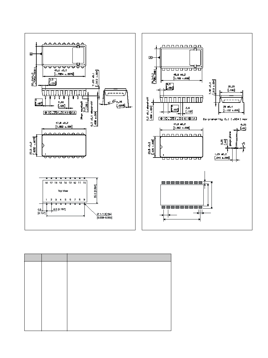
Connections
Case
The case consists of semiconductor grade
epoxy with embedded pins.
Coefficient of thermal expansion (CTE) is
typ. 15 ppm/∞C.
Weight
Maximum 20 g (0.71 oz).
Connection Pins
Base material is copper (Cu), first plating is
nickel (Ni) and second (outer) plating is
palladium (Pd).
Pin
Designation
Function
1
Out 1
Output 1. Positive voltage ref. to Rtn.
2
Rtn
Output return.
3≠6
NC
Not connected.
7
Sync
Synchronization input.
8
V
adj
Output voltage adjust. To set typical output voltage (V
Oi
)
connect pin 8 to pin 9.
9
NOR
Connection of Nominal Output voltage Resistor. (See output
voltage adjust p. 12).
10
Aux
Internally connected to pin 11.
11
RC
Remote control and turn-on/off input voltage adjust. Used to turn-on
and turn-off output.
12≠16
NC
Not connected.
17
≠In
Negative input.
18
+In
Positive input.
Mechanical Data
Through-hole version
Foot print Component side
Dimensions in mm (in)
3.6 [0.142]
5.0 [0.197]
24.0
[0.945]
29.6
[1.165]
2.8
[0.110]
1 2
3 4 5 6 7 8 9
10
11
12
13
14
15
16
17
18
40.0 [1.575]
Dimensions in mm (in)
Surface-mount version
40.0 [1.575]
Foot print Component side
4
EN/LZT 146 32 R1A (Replaces EN/LZT 137 27 R3) © Ericsson Microelectronics, June 2000
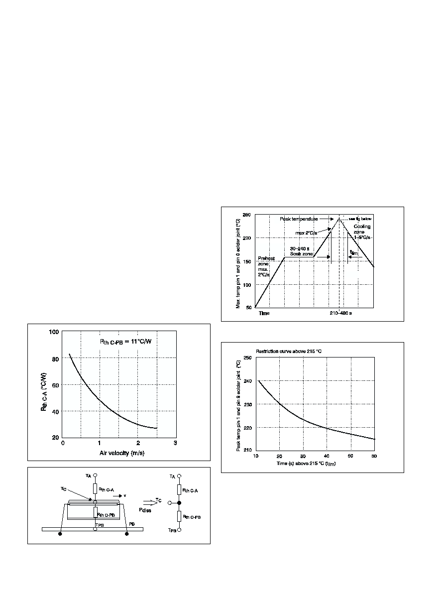
Thermal Data
Over-temperature protection
The PKF 5000 series will automatically shut down when the internal
junction temperature of the control IC in the converter reaches typ.
150 ∞C.
It will automatically re-start when the junction temperature cools
below typ. 140 ∞C.
Palladium plating is used on the terminal pins. A pin temperature (T
p
)
in excess of the solder fusing temperature (+183∞C for Sn/Pb 63/37)
for more than 25 seconds and a peak temperature above 195∞C, is
required to guarantee a reliable solder joint.
Both pin 1 and pin 9 must be monitored.
No responsibility is assumed if these recommendations are not
strictly followed.
Reflow Soldering Information
The PKF series of DC/DC power modules are manufactured in surface
mount technology. Extra precautions must therefore be taken when
reflow soldering the surface mount version. Neglecting the soldering
information given below may result in permanent damage or signifi-
cant degradation of power module performance.
The PKF series can be reflow soldered using IR, Natural Convection,
Forced Convection or Combined IR/Convection Technologies. The high
thermal mass of the component and its effect on
DT (∞C) requires that
particular attention be paid to other temperature sensitive components.
IR Reflow technology may require the overall profile time to be ex-
tended to approximately 8≠10 minutes to ensure an acceptable
DT.
Higher activity flux may be more suitable to overcome the increase in
oxidation and to avoid flux burn-up.
The general profile parameters detailed in the diagram, with this ex-
tended time to reach peak temperatures, would then be suitable.
Note! These are maximum parameters. Depending on process varia-
tions, an appropriate margin must be added.
Two-parameter model
This model provides a more precise description of the thermal charac-
teristics to be used for thermal calculations.
Thermally the power module can be considered as a component and
the case temperature can be used to characterize the properties. The
thermal data for a power module with the substrate in contact with
the case can be described with two thermal resistances. One from the
case to ambient air and one from case to PB (Printed Board).
The thermal characteristics can be calculated from the following
formula:
T
PB
= (T
C
≠T
A
)◊(R
th C≠PB
+R
th C≠A
)/R
th C≠A
≠P
d
◊R
th C≠PB
+T
A
Where:
P
d
:
dissipated power, calculated as P
O
◊(l/
h≠1)
T
C
:
max average case temperature
T
A
:
ambient air temperature at the lower side of the power
module
T
PB
:
temperature in the PB between the PKF connection pins
R
th C-PB
: thermal resistance from case to PB under the power
module
R
th C-A
:
thermal resistance from case to ambient air
v:
velocity of ambient air.
R
th C-PB
is constant and R
th
C-A
is dependent on the air velocity.
Free convection is equal to an air velocity of approx. 0.2 ≠ 0.3 m/s.
See figure below.

5
EN/LZT 146 32 R1A (Replaces EN/LZT 137 27 R3) © Ericsson Microelectronics, June 2000
Safety
The PKF Series DC/DC power modules are designed in accordance
with EN 60 950, Safety of information technology equipment including
electrical business equipment. SEMKO approval pending.
The DC/DC power module shall be installed in an end-use equip-
ment and considerations should be given to measuring the case tem-
perature to comply with T
Cmax
when in operation. Abnormal compo-
nent tests are conducted with the input protected by an external 3 A
fuse. The need for repeating these tests in the end-use appliance shall
be considered if installed in a circuit having higher rated devices.
When the supply to the DC/DC power module meets all the require-
ments for SELV (<60 V dc), the output is considered to remain within
SELV limits (level 3). The isolation is an operational insulation in
accordance with EN 60 950.
The DC/DC power module is intended to be supplied by isolated
secondary circuitry and shall be installed in compliance with the
requirements of the ultimate application. If they are connected to a
60 V DC system reinforced insulation must be provided in the power
supply that isolates the input from the mains. Single fault testing in
the power supply must be performed in combination with the
DC/DC power module to demonstrate that the output meets the
requirement for SELV. One pole of the input and one pole of the
output is to be grounded or both are to be kept floating.
The terminal pins are only intended for connection to mating con-
nectors of internal wiring inside the end-use equipment.
These DC/DC power modules may be used in telephone equipment
in accordance with paragraph 34 A.1 of UL 1459 (Standard for Tele-
phone Equipment, second edition).
The galvanic isolation is verified in an electric strength test. Test
voltage (V
ISO
) between input and output is 1,500 V dc for 60 s. In
production the test duration is decreased to 1 s.
The capacitor between input and output has a value of 1 nF and the
leakage current is less than 1µA @ 53 V dc.
The case is designed in non-conductive epoxy. Its flammability
rating meets UL 94V-0. The oxygen index is 34%
.
Fundamental circuit diagrams
Single output
Electrical Data
Transient input voltage
Single voltage pulse at +25 ∞C ambient temperature
.