
e
1
PTB 20230
45 Watts, 1.8≠2.0 GHz
PCN/PCS Power Transistor
20230
LOT CODE
0
10
20
30
40
50
60
70
0
2
4
6
8
10
Input Power (Watts)
Output Power (Watts)
V
CC
= 26 V
I
CQ
= 250 mA
f = 2.0 GHz
Typical Output Power vs. Input Power
Package 20234
Description
The 20230 is a class AB, NPN common emitter RF power transistor
intended for 26 Vdc operation from 1.8 to 2.0 GHz. Rated at 45 watts
minimum output power for PEP applications, it is specifically intended
for operation as a final or driver stage in CDMA or TDMA systems.
Ion implantation, nitride surface passivation and gold metallization
ensure excellent device reliability. 100% lot traceability is standard.
45 Watts, 1.8≠2.0 GHz
Class AB Characteristics
45% Collector Efficiency at 45 Watts
Gold Metallization
Silicon Nitride Passivated
Maximum Ratings
Parameter
Symbol
Value
Unit
Collector-Emitter Voltage
V
CER
55
Vdc
Collector-Base Voltage
V
CBO
55
Vdc
Emitter-Base Voltage (collector open)
V
EBO
4.0
Vdc
Collector Current (continuous)
I
C
7.7
Adc
Total Device Dissipation at Tflange = 25∞ C
P
D
200
Watts
Above 25∞C derate by
1.2
W/∞C
Storage Temperature Range
T
STG
≠40 to +150
∞C
Thermal Resistance (Tflange = 70∞ C)
R
JC
0.85
∞C/W
9/28/98
PTB 20230
2
e
7
8
9
10
11
12
1750
1800
1850
1900
1950
2000
2050
Frequency (MHz)
Ga
i
n
20
30
40
50
60
70
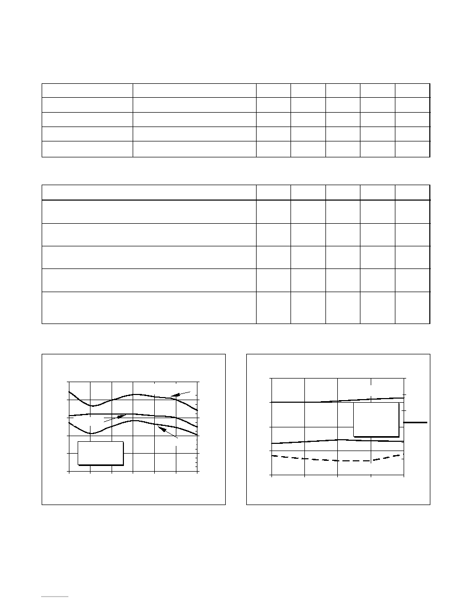
Output Power & Efficiency
V
CC
= 26 V
I
CQ
= 250 mA
P
OUT
, Gain & Efficiency
(at P-1dB)
vs. Frequency
Output Power (W)
Efficiency (%)
Gain (dB)
Broadband Test Fixture Performance
4
8
12
16
20
1900
1925
1950
1975
2000
Frequency (MHz)
G
a
in (dB)
0
10
20
30
40
50
60
V
CC
= 26 V
I
CQ
= 250 mA
P
OUT
= 45 W
Gain (dB)
Return Loss (dB)
Efficiency (%)
Efficiency (%
)
Return Loss (dB
)
- 5
-15
-25
-35
Electrical Characteristics
(100% Tested)
Characteristic
Conditions
Symbol
Min
Typ
Max
Units
Breakdown Voltage C to E
V
BE
= 0 V, I
C
= 100 mA
V
(BR)CES
55
--
--
Volts
Breakdown Voltage C to E
I
B
= 0 A, I
C
= 100 mA, R
BE
= 22
V
(BR)CER
55
--
--
Volts
Breakdown Voltage E to B
I
C
= 0 A, I
E
= 5 mA
V
(BR)EBO
4.0
5.0
--
Volts
DC Current Gain
V
CE
= 5 V, I
C
= 1 A
h
FE
20
40
--
--
RF Specifications
(100% Tested)
Characteristic
Symbol
Min
Typ
Max
Units
Gain
(V
CC
= 26 Vdc, P
OUT
= 45 W, I
CQ
= 250 mA, f = 2 GHz)
G
pe
8.5
9.5
--
dB
Gain Compression
(V
CC
= 26 Vdc, I
CQ
= 250 mA, f = 2 GHz)
P-1dB
45
--
--
Watts
Input Return Loss
(V
CC
= 26 Vdc, P
OUT
= 45 W, I
CQ
= 250 mA, f = 2 GHz)
Rtn Loss
10
--
--
dB
Collector Efficiency
(V
CC
= 26 Vdc, P
OUT
= 45 W, I
CQ
= 250 mA, f = 2 GHz)
C
45
50
--
%
Load Mismatch Tolerance
(V
CC
= 26 Vdc, P
OUT
= 45 W, I
CQ
= 250 mA,
--
--
3:1
--
f = 2 GHz--all phase angles at frequency of test)
Typical Performance
4/28/98

PTB 20230
3
e
Z Source
Z Load
Frequency
Z Source
Z Load
GHz
R
jX
R
jX
1.75
3.36
-5.20
3.20
-3.10
1.80
3.57
-5.70
3.00
-2.80
1.85
5.14
-5.55
2.90
-2.50
1.90
6.60
-5.40
2.77
-2.10
1.95
8.00
-3.80
2.75
-1.80
2.00
8.95
-1.50
2.80
-1.40
2.05
7.72
0.00
2.95
-1.00
Power Gain vs. Output Power
7
8
9
10
11
0
1
10
100
Output Power (Watts)
Po
we
r Ga
i
n
(d
B)
V
CC
= 26 V
f = 2.0 GHz
I
CQ
= 250 mA
I
CQ
= 125 mA
I
CQ
= 65 mA
Output Power vs. Supply Voltage
40
45
50
55
60
65
70
22
23
24
25
26
27
Supply Voltage (Volts)
Output Power (Watts)
I
CQ
= 250 mA
f = 2.0 GHz
-70
-60
-50
-40
-30
-20
10
20
30
40
50
60
Output Power (Watts-PEP)
IM
D (dBc
)
V
CC
= 26 V
I
CQ
= 250 mA
f
1
= 1999.9 MHz
f
2
= 2000.0 MHz
Intermodulation Distortion vs. Output Power
Impedance Data
V
CC
= 26 Vdc, P
OUT
= 45 W, I
CQ
= 250 mA
Z
0
= 50
4/28/98

PTB 20230
4
e
Typical Scattering Parameters
(V
CE
= 26 V, I
C
= 1.75 A)
f
S11
S21
S12
S22
(MHz)
Mag
Ang
Mag
Ang
Mag
Ang
Mag
Ang
100
0.936
-179
1.44
77
0.002
6
0.798
-172
200
0.946
-179
1.06
70
0.002
23
0.828
-174
300
0.963
-180
0.397
34
0.003
71
0.883
-174
400
0.970
179
0.194
19
0.004
85
0.924
-175
500
0.972
179
0.100
11
0.006
89
0.943
-177
600
0.971
178
0.046
12
0.009
88
0.982
-179
700
0.972
178
0.014
55
0.011
84
1.00
177
800
0.975
178
0.026
130
0.012
83
0.952
175
900
0.980
177
0.048
137
0.014
83
0.923
174
1000
0.980
177
0.069
135
0.017
80
0.895
174
1100
0.984
176
0.090
132
0.019
74
0.898
175
1200
0.986
176
0.113
128
0.019
72
0.897
174
1300
0.994
175
0.144
124
0.020
74
0.892
174
1400
1.00
173
0.186
119
0.023
75
0.885
174
1500
0.995
171
0.247
113
0.028
72
0.881
173
1600
0.976
169
0.350
105
0.034
67
0.875
172
1700
0.952
166
0.585
92
0.043
57
0.856
170
1800
0.757
162
1.02
48
0.052
23
0.751
171
1900
0.682
176
1.02
5
0.038
-7
0.756
178
2000
0.825
-171
0.979
-43
0.019
-55
0.848
-178
2100
0.965
-177
0.526
-76
0.004
67
0.897
178
2200
0.994
180
0.355
-87
0.009
94
0.908
177
Ericsson Components
RF Power Products
675 Jarvis Drive
Morgan Hill, CA 95037 USA
Telephone: 408-778-9434
Specifications subject to change without notice.
L1
© 1997 Ericsson Inc.
EUS/KR 1301-PTB 20230 Uen Rev. A 09-28-98
1-877-GOLDMOS
(1-877-465-3667)
e-mail: rfpower@ericsson.com
www.ericsson.com/rfpower
4/28/98