e
1
Maximum Ratings
Parameter
Symbol
Value
Unit
Drain-Source Voltage
V
DSS
65
Vdc
Gate-Source Voltage
V
GS
±20
Vdc
Operating Junction Temperature
T
J
200
∞C
Total Device Dissipation at Tflange = 25∞C
P
D
55
Watts
Above 25∞C derate by
0.31
W/∞C
Storage Temperature Range
T
STG
≠40 to +150
∞C
Thermal Resistance (Tflange = 70∞C)
R
q
JC
3.2
∞C/W
∑
INTERNALLY MATCHED
∑
Performance at 2.17 GHz, 28 Volts
- Output Power = 12 Watts Min
- Power Gain = 11 dB Typ
- Efficiency = 43% Typ @ P-1dB
∑
Full Gold Metallization
∑
Silicon Nitride Passivated
∑
Back Side Common Source
∑
Excellent Thermal Stability
∑
100% lot traceability
PTF 10119
12 Watts, 2.1≠2.2 GHz
GOLDMOS
TM
Field Effect Transistor
10119
A-1234560053
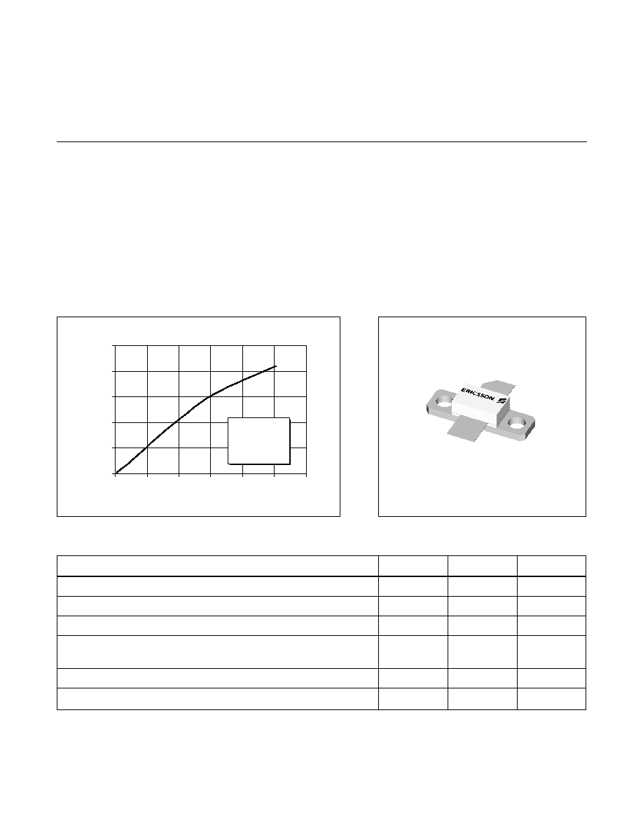
0
4
8
12
16
20
0
0.2
0.4
0.6
0.8
1
1.2
Input Power (Watts)
Output Power (Watts)
V
DD
= 28 V
I
DQ
= 160 mA
f = 2170 MHz
Typical Output Power vs. Input Power
Package 20222
Description
The PTF 10119 is an internally matched, common source, N-channel
enhancement-mode lateral MOSFET intended for WCDMA
applications from 2.1 to 2.2 GHz. It is rated at 12 watts power output.
Nitride surface passivation and gold metallization ensure excellent
device reliability.
PTF 10119
2
e
Electrical Characteristics
(100% Tested)
Characteristic
Conditions
Symbol
Min
Typ
Max
Units
Drain-Source Breakdown Voltage V
GS
= 0 V, I
D
= 50 mA
V
(BR)DSS
65
--
--
Volts
Zero Gate Voltage Drain Current
V
DS
= 26 V, V
GS
= 0 V
I
DSS
--
--
1.0
mA
Gate Threshold Voltage
V
DS
= 10 V, I
D
= 75 mA
V
GS(th)
3.0
--
5.0
Volts
Forward Transconductance
V
DS
= 10 V, I
D
= 2 A
g
fs
--
0.8
--
Siemens
RF Specifications
(100% Tested)
Characteristic
Symbol
Min
Typ
Max
Units
Gain
(V
DD
= 28 V, P
OUT
= 3 W, I
DQ
= 160 mA, f = 2.11, 2.17 GHz)
G
ps
10
11
--
dB
Power Output at 1 dB Compressed
(V
DD
= 28 V, I
DQ
= 160 mA, f = 2.17 GHz)
p-1dB
12
14
--
Watts
Drain Efficiency
(V
DD
= 28 V, P
OUT
= 12 W, I
DQ
= 160 mA, f = 2.17 GHz)
h
D
30
43
--
%
Load Mismatch Tolerance
(V
DD
= 28 V, P
OUT
= 12 W, I
DQ
= 160 mA, f = 2.17 GHz
Y
--
--
10:1
--
--all phase angles at frequency of test)
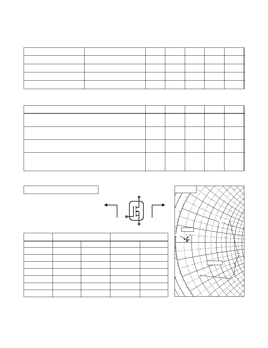
Impedance Data
V
DS
= 28 V, P
OUT
= 12 W, I
DQ
= 160 mA
Frequency
Z Source
W
Z Load
W
GHz
R
jX
R
jX
2.00
5.7
-12.11
3.30
1.21
2.10
16.4
-19.50
3.55
0.92
2.12
19.7
-18.82
4.12
0.88
2.15
22.8
-14.14
3.75
0.62
2.17
23.0
-13.15
3.53
0.34
2.20
26.6
-9.28
3.32
0.38
2.30
20.2
12.03
3.23
0.84
Z Source
Z Load
G
S
D
0.
1
0.
3
0.
5
0.
2
0.
4
0.1
0.3
0.2
0.1
0.3
0.2
0
05
0.
45
<
--
-
W
A
V
E
L
0
.
0
Z Source
2.00 GHz
2.30 GHz
Z Load
2.30 GHz
2.00 GHz
Z
0
= 50
W
PTF 10119
3
e
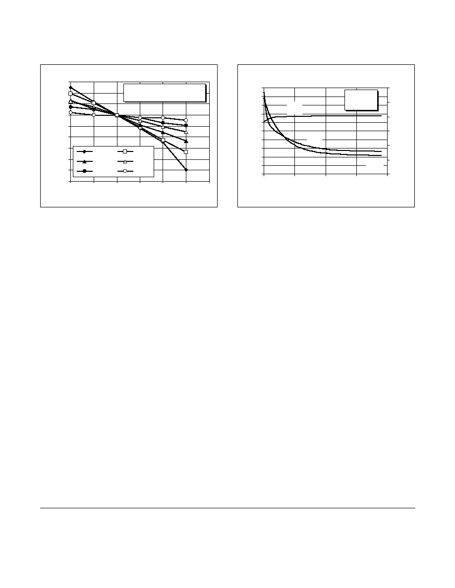
Capacitance vs. Supply Voltage *
0
5
10
15
20
25
30
35
40
45
50
0
10
20
30
40
Supply Voltage (Volts)
Cds and Cgs (pF)
0
0.5
1
1.5
2
2.5
3
Crss (pF)
C
gs
C
ds
C
rss
V
GS
= 0 V
f = 1 MHz
*This part is internally matched. Measurements of the finished
product will not yield these figures.
Bias Voltage vs. Temperature
0.94
0.95
0.96
0.97
0.98
0.99
1.00
1.01
1.02
1.03
-20
0
20
40
60
80
100
Temp. (∞C)
Bias Voltage (V)
0.075
0.2875
0.5
0.7125
0.925
1.1375
Voltage nomalized to 1.0 V
Series show current (A)
Ericsson Microelectronics
RF Power Products
Morgan Hill, CA 95037 USA
Specifications subject to change without notice.
L1
© 1998 Ericsson Inc.
EUS/KR 1301-PTF 10119 Uen Rev. A 12-21-99
1-877-GOLDMOS (465-3667) United States
+46 8 757 4700 International
e-mail: rfpower@ericsson.com
www.ericsson.com/rfpower
