 | –≠–ª–µ–∫—Ç—Ä–æ–Ω–Ω—ã–π –∫–æ–º–ø–æ–Ω–µ–Ω—Ç: PTF10125 | –°–∫–∞—á–∞—Ç—å:  PDF PDF  ZIP ZIP |

e
1
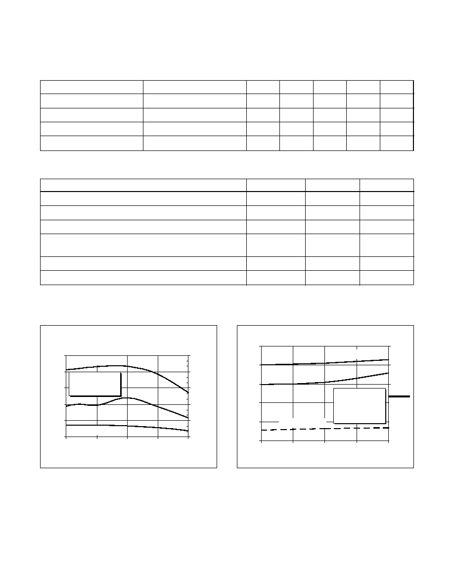
RF Specifications
(100% Tested)
Characteristic
Symbol
Min
Typ
Max
Units
Gain
(V
DD
= 28 V, P
OUT
= 30 W, I
DQ
= 1.3 A Total,
G
ps
11.5
12.5
--
dB
f = 1.50, 1.55 GHz)
Power Output at 1 dB Compression
(V
DD
= 28 V, I
DQ
= 1.3 A Total, f = 1.50, 1.55 GHz)
P-1dB
135
150
--
Watts
Drain Efficiency
(V
DD
= 28 V, P
OUT
= 135 W, I
DQ
= 1.3 A Total, f = 1.5 GHz)
h
D
35
40
--
%
Load Mismatch Tolerance
(V
DD
= 28 V, P
OUT
= 67.5 W, I
DQ
= 1.3 A Total, f = 1.5 GHz
Y
--
--
10:1
--
--all phase angles at frequency of test)
All published data at T
CASE
= 25∞C unless otherwise indicated.
PTF 10125
135 Watts, 1.4≠1.6 GHz
GOLDMOS
TM
Field Effect Transistor
Package 20250
0
20
40
60
80
100
120
140
160
180
200
0
3
6
9
12
15
Input Power (Watts)
Output Power (Watts
)
V
DD
= 28 V
I
DQ
= 1.3 A Total
f = 1500 MHz
Typical Output Power vs. Input Power
Description
The PTF 10125 is an internally matched, common source N-channel
enhancement-mode lateral MOSFET intended for linear driver and
final applications from 1.4 to 1.6 GHz, such as DAB/DRB. It is rated
at 135 watts minimum power outpt. Nitride surface passivation and
full gold metallization ensure excellent device lifetime and reliability.
∑
INTERNALLY MATCHED
∑
Performance at 1.5 GHz, 28 V
- Output Power = 135 Watts Min
- Power Gain = 12.5 dB Typ
∑
Full Gold Metallization
∑
Silicon Nitride Passivated
∑
Back Side Common Source
∑
Excellent Thermal Stability
∑
100% Lot Traceability
10125
A-1234569935
PTF 10125
2
e
Electrical Characteristics
(100% Tested--characteristics, conditions and limits shown per side)
Characteristic
Conditions
Symbol
Min
Typ
Max
Units
Drain-Source Breakdown Voltage V
GS
= 0 V, I
D
= 100 mA
V
(BR)DSS
65
--
--
Volts
Zero Gate Voltage Drain Current
V
DS
= 28 V, V
GS
= 0 V
I
DSS
--
--
5.0
mA
Gate Threshold Voltage
V
DS
= 10 V, I
D
= 150 mA
V
GS(th)
3.0
--
5.0
Volts
Forward Transconductance
V
DS
= 10 V, I
D
= 6 A
g
fs
2.0
4.0
--
Siemens
Maximum Ratings
Parameter
Symbol
Value
Unit
Drain-Source Voltage
(1)
V
DSS
65
Vdc
Gate-Source Voltage
(1)
V
GS
±20
Vdc
Operating Junction Temperature
T
J
200
∞C
Total Device Dissipation
P
D
440
Watts
Above 25∞C derate by
2.51
W/∞C
Storage Temperature Range
T
STG
≠40 to +150
∞C
Thermal Resistance (T
CASE
= 70∞C)
R
q
JC
0.39
∞C/W
(1)
per side
Typical Performance
12
13
14
15
16
17
1400
1450
1500
1550
1600
Frequency (MHz)
G
a
in (dB)
30
60
90
120
150
180
Output Power & Efficienc
y
V
DD
= 28 V
I
DQ
= 1.3 A Total
Typical P
OUT
, Gain & Efficiency
(at P-1dB)
vs. Frequency
Output Power (W)
Efficiency (%)
Gain (dB)
Broadband Test Fixture Performance
6
8
10
12
14
16
1450
1475
1500
1525
1550
Frequency (MHz)
G
a
in (dB)
0
10
20
30
40
50
V
DD
= 28 V
I
DQ
= 1.3 A Total
P
OUT
= 135 W
Gain
Return Loss (dB)
Efficiency (%)
Efficienc
y
Re
turn Los
s
-10
-15
-20

PTF 10125
3
e
Power Gain vs. Output Power
9
10
11
12
13
14
10
100
1000
Output Power (Watts)
Po
we
r Ga
i
n
(d
B)
I
DQ
= 650 mA
V
DD
= 28 V
f = 1500 MHz
I
DQ
= 1300 mA
I
DQ
= 325 mA
100
120
140
160
180
200
24
26
28
30
32
Supply Voltage (Volts)
Output Power (Watts)
I
DQ
= 1.3 A Total
f = 1500 MHz
Output Power
(P-1dB)
vs. Supply Voltage
-70
-60
-50
-40
-30
-20
-10
0
50
100
150
200
Output Power (Watts-PEP)
IM
D (dBc
)
V
DD
= 28 V, I
DQ
= 1.3 A Total
f
1
= 1500.0 MHz, f
2
= 1500.1 MHz
Intermodulation Distortion vs. Output Power
(as measured in a broadband circuit)
3rd Order
7th
5th
0
50
100
150
200
250
0
10
20
30
40
Supply Voltage (Volts)
Cds and Cgs (pF)
0
2
4
6
8
10
C
r
ss (pF)
C
gs
C
ds
C
rss
V
GS
= 0 V
f = 1 MHz
Capacitance vs. Supply Voltage
(per side)
*
* This part is internally matched. Measurements of the finished
product will not yield these results.
0
2
4
6
8
10
12
14
0
10
20
30
40
50
60
Average Output Power (Watts)
10 dB Peak to Average
Peak Pow
e
r
G
a
in (dB
)
V
DD
= 28 V
I
DQ
= 1.3 A Total
f = 1500 MHz
Peak Power Gain for DAB Applications
@ 10% Pulsed Input Signal
10% Pulse Conditions
f = 20 KHz
Pulse Width = 5 us
Bias Voltage vs. Temperature
0.95
0.96
0.97
0.98
0.99
1.00
1.01
1.02
1.03
-20
30
80
130
Temp. (∞C)
B
i
as Voltage (V
)
0.6
1.74
2.88
4.02
5.16
6.3
Voltage normalized to 1.0 V
Series show current (A)

PTF 10125
4
e
Impedance Data
(V
DD
= 28 V, P
OUT
= 135 W,
I
DQ
= 1.3 A Total)
Frequency
Z Source
W
Z Load
W
GHz
R
jX
R
jX
1400
2.85
-4.23
2.60
-2.46
1450
4.16
-4.36
2.36
-2.53
1500
4.58
-3.30
2.04
-2.48
1550
4.02
-0.83
1.63
-2.52
1600
3.41
0.37
1.27
-2.08
Z Source
Z Load
G
D
G
S
D
0.
1
0.1
0.1
-
W
A
V
E
L
E
N
G
T
H
S
T
O
W
AR
D
G
E
N
E
R
A
T
O
<
--
-
W
A
V
E
L
E
N
G
T
H
S
T
O
W
A
R
D
L
O
A
D
-
0
.
0
Z Load
1.6 GHz
1.6 GHz
1.4 GHz
1.4 GHz
Z Source
Z
0
= 50
W

PTF 10125
5
e
Test Circuit
Q1
PTF 10125
LDMOS RF Transistor
l
1,
l
2
Microstrip 50
W
l
3,
l
4
.25
l
@ 1.5 GHz
Microstrip 70
W
l
5,
l
6
.08
l
@ 1.5 GHz
Microstrip 80
W
l
7,
l
8
.138
l
@ 1.5 GHz
Microstrip 9.5
W
l
9,
l
10
.096
l
@ 1.5 GHz
Microstrip 7.7
W
l
11,
l
12
.045
l
@ 1.5 GHz
Microstrip 7.7
W
C1, C2, C3, C4, C7,
C8, C11, C12
13 pF Chip Cap
ATC 100 B
C5, C6, C15, C16
0.1
m
F Chip Cap
K1206
C9, C10, C13, C14 10
m
F SMT Tantalum Cap
C17, C19
2.0 pF Chip Cap
ATC 100 B
C18
0.3 pF Chip Cap
ATC 100 B
L1, L2
2.7 nh SMT Coil
L3, L4
4 mm SMT Ferrite Bead
R1, R2, R3, R4
220
W
Chip Resistor
K1206
R5, R6
2K SMT Potentiometer
R7, R8
10
W
Chip Resistor
K1206
R9, R10
1
W
Chip Resistor
K1206
T1, T2
50
W
Coaxial Balun
Circuit Board
.028" Dielectric Thickness,
e
r
= 4.0,
AlliedSignal, G200, 2 oz. copper
Test Circuit Block Diagram for f = 1.5 GHz

PTF 10125
6
e
Parts Layout (not to scale)
Artwork (1 inch
)
Ericsson Microelectronics
RF Power Products
Morgan Hill, CA 95037 USA
Specifications subject to change without notice.
L3
© 1998 Ericsson Inc.
EUS/KR 1301-PTF 10125 Uen Rev. A 12-01-99
1-877-GOLDMOS (465-3667) United States
+46 8 757 4700 International
e-mail: rfpower@ericsson.com
www.ericsson.com\rfpower