 | –≠–ª–µ–∫—Ç—Ä–æ–Ω–Ω—ã–π –∫–æ–º–ø–æ–Ω–µ–Ω—Ç: PTF10153 | –°–∫–∞—á–∞—Ç—å:  PDF PDF  ZIP ZIP |
e
1
PTF 10153
60 Watts, 1.8≠2.0 GHz
GOLDMOS
Æ
Field Effect Transistor
Package 20248
0
10
20
30
40
50
60
70
80
90
0
2
4
6
8
10
12
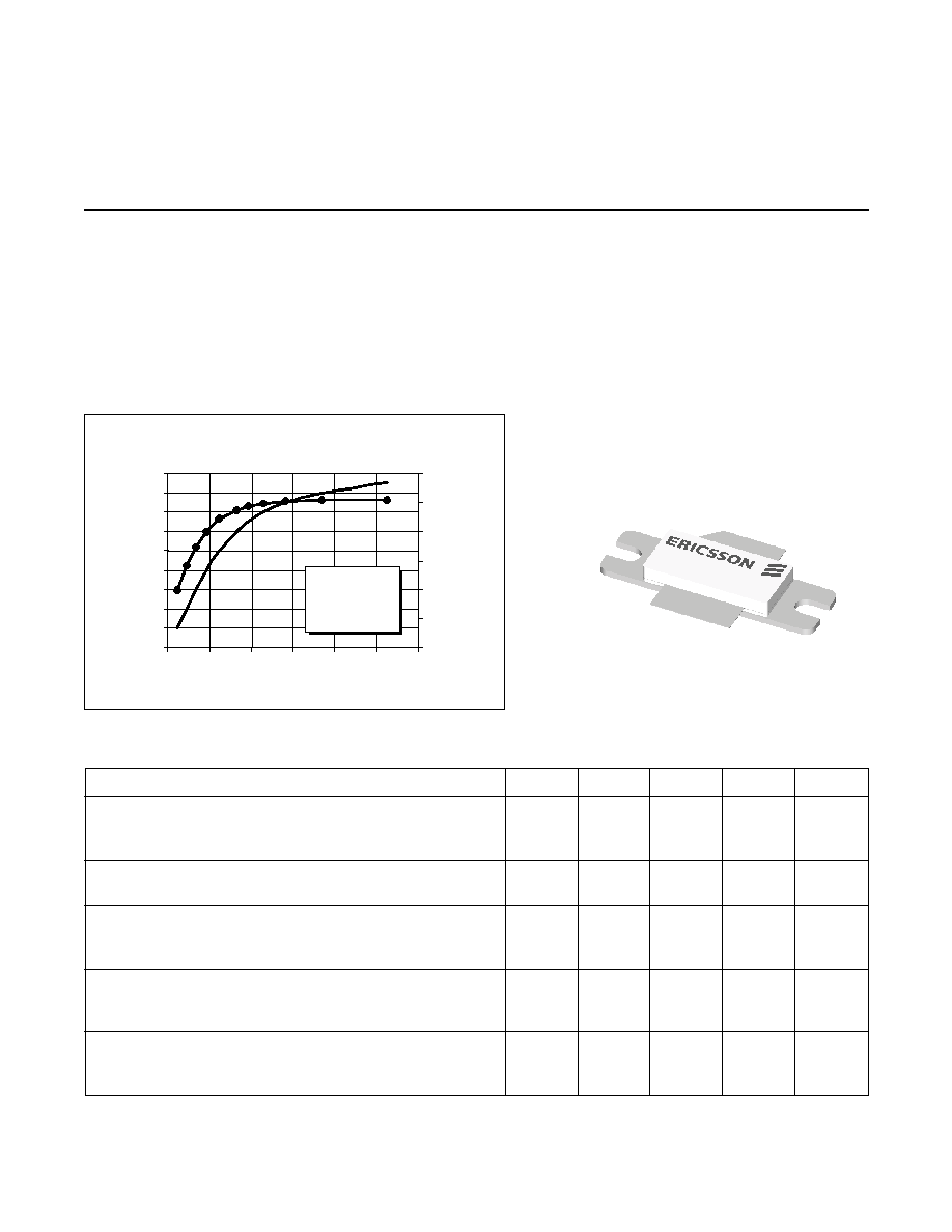
Input Power (Watts)
O
u
tput Pow
e
r (Watts)
0
10
20
30
40
50
60
Efficiency (%)
V
DD
= 28 V
I
DQ
= 650mA
f = 1880 MHz
Typical Output Power & Efficiency
vs. Input Power
Description
The PTF 10153 is an internally matched 60≠watt GOLDMOS FET
intended for CDMA and TDMA applications from 1.8 to 2.0 GHz. It
operates with 40% efficiency and 11.5 dB minimum gain. Nitride
surface passivation and full gold metallization ensure excellent de-
vice lifetime and reliability.
∑
INTERNALLY MATCHED
∑
Guaranteed Performance at 1805, 1843, 1880
MHz, 28 V
- Output Power = 60 Watts Min
- Power Gain = 11.5 dB Min
∑
Full Gold Metallization
∑
Silicon Nitride Passivated
∑
Back Side Common Source
∑
Excellent Thermal Stability
∑
100% Lot Traceability
RF Specifications
(100% Tested)
Characteristic
Symbol
Min
Typ
Max
Units
Gain
(V
DD
= 28 V, P
OUT
= 60 W, I
DQ
= 650 mA,
G
ps
11.5
--
--
dB
f = 1805, 1843, 1880 MHz)
Power Output at 1 dB Compression
(V
DD
= 28 V, I
DQ
= 650 mA, f = 1880 MHz)
P-1dB
60
--
--
Watts
Drain Efficiency
(V
DD
= 28 V, P
OUT
= 60 W, I
DQ
= 650 mA,
h
D
40
--
--
%
f = 1805, 1843, 1880 MHz)
Return Loss
(V
DD
= 28 V, P
OUT
= 60 W, I
DQ
= 650 mA,
--
--
--
≠9.5
dB
f = 1805, 1843, 1880 MHz)
Load Mismatch Tolerance
(V
DD
= 28 V, P
OUT
= 60 W, I
DQ
= 650 mA, f = 1805
Y
--
--
10:1
--
--all phase angles at frequency of test)
All published data at T
CASE
= 25∞C unless otherwise indicated.
10153
A-1234569953
PTF 10153
2
e
7
8
9
10
11
12
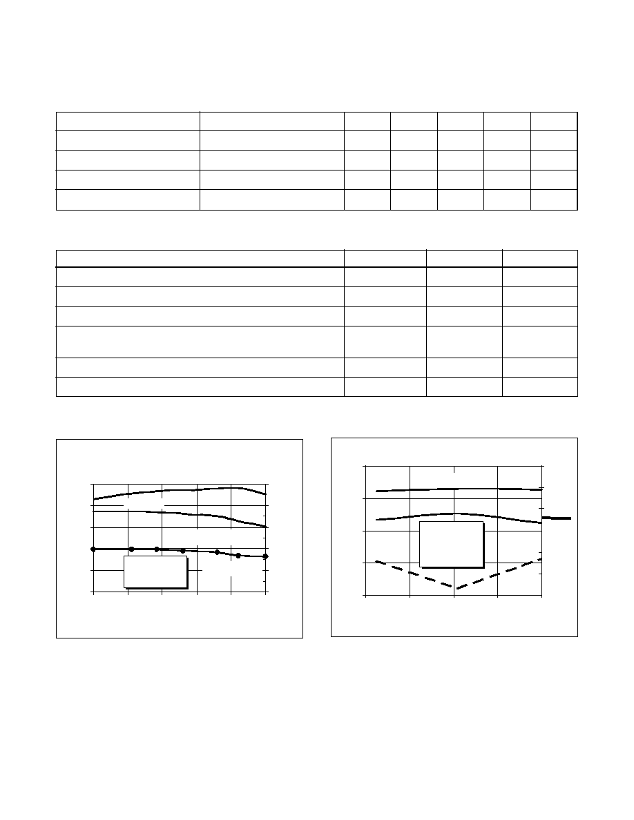
1750
1800
1850
1900
1950
2000
Frequency (MHz)
Ga
in
20
34
48
62
76
90
O
u
tp
u
t
Po
w
e
r & Effi
ci
en
cy
V
DD
= 28 V
I
DQ
= 650 mA
Typical P
OUT
, Gain & Efficiency
(at P-1dB)
vs. Frequency
Output Pow er (W)
Efficiency (%)
Gain (dB)
Broadband Test Fixture Performance
4
8
12
16
20
1800
1820
1840
1860
1880
Frequency (MHz)
G
a
in
(
d
B)
0
10
20
30
40
50
60
V
DD
= 28V
I
DQ
= 650 mA
P
OUT
= 60 W
Gain
Return Loss (dB)
Efficiency (%)
E
ffi
ci
ency
R
e
turn Loss
- 5
-10
-15
-25
Electrical Characteristics
(100% Tested)
Characteristic
Conditions
Symbol
Min
Typ
Max
Units
Drain-Source Breakdown Voltage
V
GS
= 0 V, I
D
= 25 mA
V
(BR)DSS
65
--
--
Volts
Zero Gate Voltage Drain Current
V
DS
= 28 V, V
GS
= 0 V
I
DSS
--
--
1
mA
Gate Threshold Voltage
V
DS
= 10 V, I
D
= 75 mA
V
GS(th)
3.0
--
5.0
Volts
Forward Transconductance
V
DS
= 10 V, I
D
= 0.5 A
g
fs
1.0
--
--
Siemens
Maximum Ratings
Parameter
Symbol
Value
Unit
Drain-Source Voltage
V
DSS
65
Vdc
Gate-Source Voltage
V
GS
±20
Vdc
Operating Junction Temperature
T
J
200
∞C
Total Device Dissipation at
P
D
237
Watts
Above 25∞C derate by
1.35
W/∞C
Storage Temperature Range
T
STG
≠40 to +150
∞C
Thermal Resistance (T
CASE
= 70∞C)
R
q
JC
0.74
∞C/W
Typical Performance
PTF 10153
3
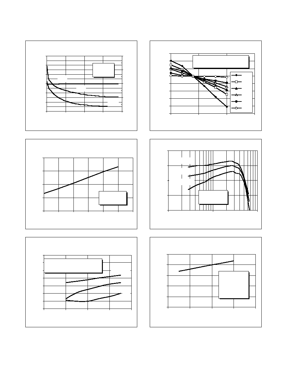
e
20
40
60
80
100
24
26
28
30
32
34
36
Supply Voltage (Volts)
Output P
o
wer
(W
atts)
I
DQ
= 650mA
f =1880 MHz
Output Power
(@ 1 dB Compression)
vs. Supply Voltage
Power Gain vs. Output Power
12.0
12.5
13.0
13.5
14.0
1
10
100
Output Power (Watts)
P
o
wer Gai
n
(
d
B)
V
DD
= 28 V
f = 1880 MHz
I
DQ
= 650
I
DQ
= 550
I
DQ
= 450
Capacitance vs. Supply Voltage *
0
40
80
120
160
200
240
0
10
20
30
40
Supply Voltage (Volts)
Cds and Cgs (
pF)
0
6
12
18
24
Crss
C
gs
C
ds
C
rss
V
GS
= 0 V
f = 1 MHz
Bias Voltage vs. Temperature
0.95
0.96
0.97
0.98
0.99
1.00
1.01
1.02
1.03
-20
30
80
130
Temp. (∞C)
B
i
as Voltage (V)
0.400
1.383
2.367
3.350
4.333
5.317
Voltage normalized to 1.0 V
Series show current (A)
* This part is internally matched. Measurements of the finished
product will not yield these results.
-70
-60
-50
-40
-30
-20
-10
0
0
20
40
60
80
Output Power (Watts-PEP)
IM
D (d
Bc)
V
DD
= 28V, I
DQ
= 650 mA
f
1
= 1880 MHz, f
2
= 1879 MHz
Intermodulation Distortion vs. Output Power
(as measured in a broadband circuit)
3rd Order
7th
5th
-70
-60
-50
-40
-30
-20
10
30
50
70
90
Output Power (Watts-PEP)
IM
D (
d
Bc
)
V
DD
= 28 V
I
DQ
= 650 mA
f
1
= 1880 MHz
f
2
= 1879 MHz
2-Tone IMD vs. Output Power
(as measured in a broadband circuit)
PTF 10153
4
e
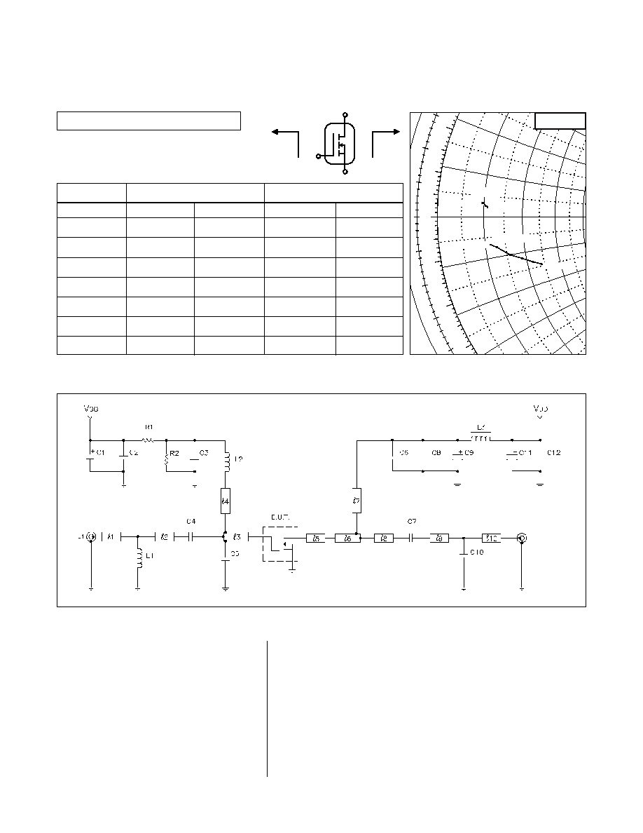
Frequency
Z Source
W
Z Load
W
MHz
R
jX
R
jX
1805
2.27
-3.40
2.12
1.20
1842
3.05
-3.86
1.97
1.31
1880
4.07
-4.04
1.88
1.31
1930
4.56
-5.10
1.59
1.68
1960
6.10
-5.90
1.46
1.74
1990
7.50
-6.75
1.48
1.61
2000
8.75
-7.40
1.53
1.64
Impedance Data
V
DD
= 28 V, P
OUT
= 60 W, I
DQ
= 650 mA
Z Source
Z Load
G
S
D
0.1
0.3
0.2
0.4
0.1
0.2
0.1
.3
0.2
-
W
A
V
E
L
E
N
G
T
H
S
T
O
W
A
R
D
G
E
N
E
R
A
T
O
R
-
--
>
<
-
--
W
A
V
E
L
E
N
G
T
H
S
T
O
W
A
R
D
L
O
A
D
-
0
.
0
1805 MHz
2000 MHz
Z Load
Z Source
2000 MHz
1805 MHz
Z
0
= 50
W
Test Circuit
Block Diagram for f = 2 GHz
D.U.T.
PTF 10153
NPN RF Transistor
l
1
0.086
l
2 GHz
Microstrip
50
W
l
2
0.132
l
2 GHz
Microstrip
50
W
l
3
0.112
l
2 GHz
Microstrip
9.24
W
l
4
0.064
l
2 GHz
Microstrip
78
W
l
5
0.127
l
2 GHz
Microstrip
6.64
W
l
6
0.041
l
2 GHz
Microstrip
9.24
W
l
7
0.206
l
2 GHz
Microstrip
65
W
l
8
0.077
l
2 GHz
Microstrip
21.87
W
l
9
0.070
l
2 GHz
Microstrip
50
W
l
10
0.028
l
2 GHz
Microstrip
50
W
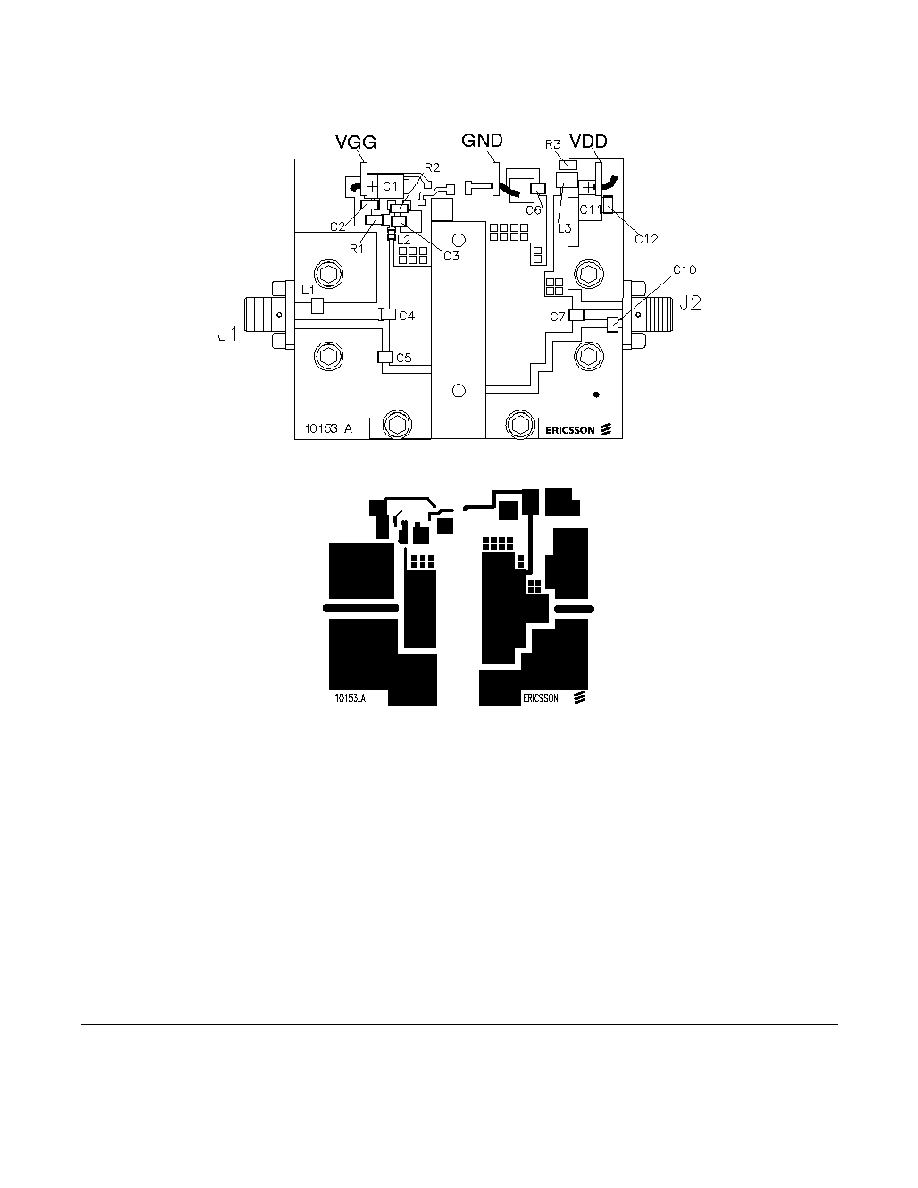
C1, C11
Capicitor, 10 µF
ATC 100 B
C2
Capicitor, 0.1 µF, 50 V
Digi-Key PCC103BCT
C3, C6, C4, C7
Capicitor, 10 pF
ATC 100 B
C5
Capicitor, 1.1 pF
ATC 100 B
C10
Capicitor, 0.30 pF
ATC 100 B
C12
Capicitor, 0.1 µF
ATC 100 B
R1, R2
Resistor, 220
W
Digi-Key 2.2QBK
R3
Resistor, 1.0
W
Digi-Key, # P1OCT
L1
Chip Inductor, 8 µH
Coilcraft A03T
L2
Chip Inductor, 2.7 µH
N/A
L3
Ferrite, 6 mm
N/A
PCB
0.050",
e
r
= 6.0, 2 oz. Copper, TMM6, Rogers Corporation
PTF 10153
5
e
Artwork (not to scale)
Assembly Diagram (not to scale)
Ericsson Inc.
Microelectronics
Morgan Hill, CA 95037 USA
Specifications subject to change without notice.
L3
© 1999, 2000 Ericsson Inc.
EUS/KR 1522-PTF 10153 Uen Rev. B 11-06-00
1877-GOLDMOS (465-3667) United States
+46 8 757 4700 International
e-mail: rfpower@ericsson.com
www.ericsson.com/rfpower