
EFST
F49B002UA
Elite Flash Storage Technology Inc.
Publication Date : Jun. 2003
Revision: 1.2 1/33
2 Mbit (128K x 8)
5V Only CMOS Flash Memory
1. FEATURES
Single supply voltage 5V ± 10%
Fast access time: 70/90 ns
Compatible with JEDEC standard
- Pin-out, packages and software commands
compatible with single-power supply Flash
Low power consumption
- 25mA maximum active current
- 25uA typical standby current
10,000 minimum program/erase cycles
Command register architecture
- Byte programming (10us typical)
- Sector Erase( sector structure: 16KB, 8KB, 8KB,
96KB, 128KB )
Auto Erase (chip & sector) and Auto Program
- Sector erase and Chip erase.
- Automatically program and verify data at specified
address
End of program or erase detection
- Data polling
- Toggle bits
Boot Sector Architecture
- U = Upper Boot Sector
Packages available:
- 32-pin PDIP
- 32-pin PLCC
2. ORDERING INFORMATION
Part No
Boot
Speed
Package
Part No
Boot
Speed
Package
F49B002UA-70D
Upper
70 ns
PDIP
F49B002UA-90D
Upper
90 ns
PDIP
F49B002UA-70N
Upper
70 ns
PLCC
F49B002UA-90N
Upper
90 ns
PLCC
3. GENERAL DESCRIPTION
The F49B002UA is a 2 Megabit, 5V only CMOS Flash
memory device organized as 128K bytes of 8 bits. This
device is packaged in standard 32-pin PDIP and 32-pin
PLCC. It is designed to be programmed and erased both in
system and can in standard EPROM programmers.
With access times of 70 ns and 90 ns, the F49B002UA
allows the operation of high-speed microprocessors. The
device has separate chip enable CE, write enable WE ,
and output enable
OE
controls. EFST's memory devices
reliably store memory data even after 10,000 program and
erase cycles.
The F49B002UA is entirely pin and command set
compatible with the JEDEC standard for 2 Megabit Flash
memory devices. Commands are written to the command
register using standard microprocessor write timings.
The F49B002UA features a sector erase architecture.
The device memory array is divided into 16 Kbytes, 8K
bytes, 8Kbytes, 96Kbytes, 128Kbytes. Erase capabilities
provide the flexibility to revise the data in the device.
A low V
CC
detector inhibits write operations on loss of
power. End of program or erase is detected by the Data
Polling of DQ7, or by the Toggle Bit feature on DQ6. Once
the program or erase cycle has been successfully
completed, the device internally resets to the Read mode.

EFST
F49B002UA
Elite Flash Storage Technology Inc.
Publication Date : Jun. 2003
Revision: 1.2 2/33
4. PIN CONFIGURATIONS
4.1 32-pin PDIP
4.2 32-pin PLCC
4.3 Pin Description
Symbol
Pin Name
Functions
A0~A17
Address Input
To provide memory addresses.
DQ0~DQ7
Data Input/Output
To output data when Read and receive data when Write.
The outputs are in tri-state when OE or CE is high.
CE
Chip Enable
To activate the device when CE is low.
OE
Output Enable
To gate the data output buffers.
WE
Write Enable
To control the Write operations.
NC
No connection
Unconnected pin
V
CC
Power Supply
To provide power
GND
Ground
5
6
7
8
9
10
11
12
13
A7
A6
A5
A4
A3
A2
A1
A0
DQ0
2 9
2 8
2 7
2 6
2 5
2 4
2 3
2 2
2 1
A14
A13
A8
A9
A11
OE
A10
C E
DQ7
DQ6
DQ5
DQ4
DQ3
GN
D
DQ2
DQ1
32 31 30
14 15 16 17 18 19 20
4 3 2 1
A1
7
WE
V
CC
NC
A1
6
A1
5
A1
2
1
2
3
4
5
6
7
8
9
10
11
12
13
14
15
16
N C
A16
A15
A12
A7
A6
A5
A4
A3
A2
A1
A0
DQ0
DQ1
DQ2
G N D
3 2
3 1
3 0
2 9
2 8
2 7
2 6
2 5
2 4
2 3
2 2
2 1
2 0
1 9
1 8
1 7
V
D D
W E
A17
A14
A13
A8
A9
A11
OE
A10
C E
DQ7
DQ6
DQ5
DQ4
DQ3
3 2-Pin
DIP

EFST
F49B002UA
Elite Flash Storage Technology Inc.
Publication Date : Jun. 2003
Revision: 1.2 3/33
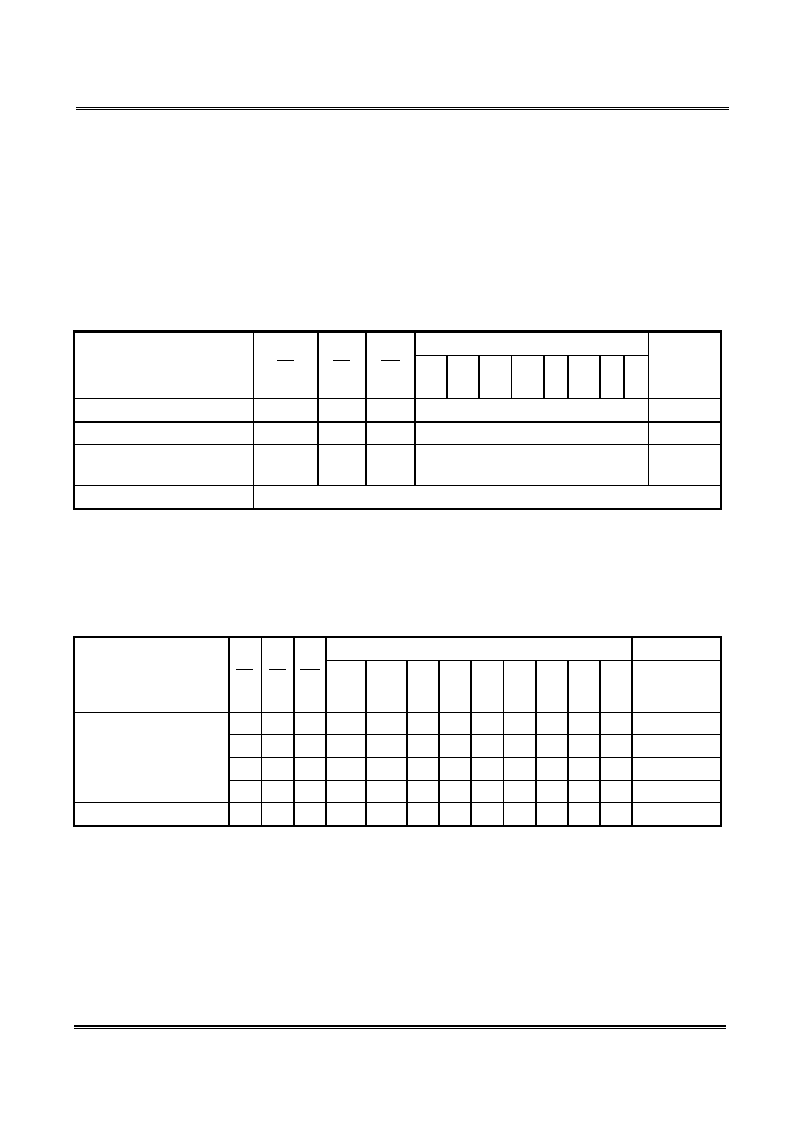
5. SECTOR STRUCTURE
Table 1: F49B002UA Sector Address Table
Sector Address
Sector
Sector Size
(Kbytes)
Address range
A17
A16
A15
A14
A13
SA4
16
3C000H-3FFFFH
1
1
1
1
X
SA3
8
3A000H-3BFFFH
1
1
1
0
1
SA2
8
38000H-39FFFH
1
1
1
0
0
SA1
96
20000H-37FFFH
1
X
X
X
X
SA0
128
00000H-1FFFFH
0
X
X
X
X
6. FUNCTIONAL BLOCK DIAGRAM
G
ND
State
control
CE
OE
WE
Decorder
V
DD
A[17:0]
B4 (Boot) 16K
B3 (Param.1) 8K
B2 (Param.2) 8K
B1 (Main1) 96K
B0 (Main2) 128K
3FFFF
3C000
3BFFF
3A000
39FFF
38000
37FFF
20000
1FFFF
00000
I/O
buffers
DQ[7:0]
EFST
F49B002UA
Elite Flash Storage Technology Inc.
Publication Date : Jun. 2003
Revision: 1.2 4/33
7. FUNCTIONAL DESCRIPTION
7.1 Device operation
This section describes the requirements and use
of the device bus operations, which are initiated
through the internal command register. The
register is composed of latches that store the
command, address and data information needed
to execute the command. The contents of the
register serve as inputs to the internal state
machine. The state machine outputs dictate the
function of the device. The F49B002UA features
various bus operations as Table 2.
Table 2. F49B002UA Operation Modes Selection
ADDRESS
DESCRIPTION
CE
OE
WE
A17
|
A13
A12
|
A10
A9
A8
|
A7
A6
A5
|
A2
A1 A0
DQ0~DQ7
Read
L
L
H
AIN
Dout
Write
L
H
L
AIN
DIN
Output Disable
L
H
H
X
High Z
Standby
H
X
X
X
High Z
Auto-select
See Table 3
Notes:
1.
L= Logic Low = V
IL
, H= Logic High = V
IH
, X= Don't Care, SA= Sector Address, AIN= Address In, DIN = Data In,
Dout = Data Out.
Table 3. F49B002UA Auto-Select Mode (High Voltage Method)
ADDRESS
DQ0~DQ7
DESCRIPTION
CE
OE
WE
A17
|
A13
A12
|
A10
A9
A8
|
A4
A6
A3
A2
A1
A0
L
L
H
X
X
V
ID
X
X
L
H
L
L
7FH
L
L
H
X
X
V
ID
X
X
H
L
L
L
7FH
L
L
H
X
X
V
ID
X
X
H
H
L
L
7FH
(Manufacturer ID:EFST)
L
L
H
X
X
V
ID
X
X
L
L
L
L
8CH
(Device ID: F49B002UA)
L
L
H
X
X
V
ID
X
X
L
L
L
H
00H
Notes :
1.Manufacturer and device codes may also be accessed via the software command sequence in Table 4.
2. V
ID
=11.5V to 12.5V.

EFST
F49B002UA
Elite Flash Storage Technology Inc.
Publication Date : Jun. 2003
Revision: 1.2 5/33
Read Mode
To read array data from the outputs, the system must
drive the CE and OE pins to V
IL
. CE is the power
control and selects the device.
OE
is the output control
and gates array data to the output pins. WE should
remain at V
IH
. The internal state machine is set for
reading array data upon device power-up, or after a
hardware reset. This ensures that no spurious alteration
of the memory content occurs during the power
transition.
No command is necessary in this mode to obtain array
data. Standard microprocessor's read cycles that assert
valid addresses on the device address inputs produce
valid data on the device data outputs. The device remains
enabled for read access until the command register
contents are altered.
See "Read Command" section for more information.
Refer to the AC Read Operations Table 9 for timing
specifications and to Figure 5 for the timing diagram. I
CC1
in the DC Characteristics Table 8 represents the active
current specification for reading array data.
Write Mode
To write a command or command sequence (which
includes programming data to the device and erasing
sectors of memory), the system must drive WE and CE to
V
IL
, and
OE
to V
IH
. The "Program Command" section has
details on programming data to the device using standard
command sequences.
An erase operation can erase one sector, or the entire
device. Table 1 indicate the address space that each sector
occupies. A "sector address" consists of the address bits
required to uniquely select a sector. The "Software
Command Definitions" section has details on erasing a
sector or the entire chip.
When the system writes the auto-select command
sequence, the device enters the auto-select mode. The
system can then read auto-select codes from the internal
register (which is separate from the memory array) on
DQ7≠DQ0. Standard read cycle timings apply in this mode.
Refer to the Auto-select Mode and Auto-select Command
sections for more information. I
CC2
in the DC Characteristics
Table 8 represents the active current specification for the
write mode. The "AC Characteristics" section contains
timing specification Table 10 and timing diagrams for write
operations.
Resetting the device
The reset command returns the device to Read mode.
This is a necessary step after reading the device or
manufacturer ID. Note: In these cases, if VID is removed
from the A9 pin, the device automatically returns to
Read mode and an explicit is not required.
Boot block looking
To keep any system kernel code secure in the boot
block, the F49B002UA provides a command to lock
the boot block and prevent any accidental erasure or
reprogramming. The command sequence is similar to
the chip erase sequence except for the last cycle,
where 40H must be written into DQ0~DQ7 instead of
10H. The boot block is the only block that can be
locked in this way.
Whether or not the boot block has been locked can be
detected by the command sequence shown in Table 4.
This command sequence returns a "1" on DQ0 if the
boot block is locked; a "0" if the boot block has not
been locked and it is open to erasing and
programming.
Output Disable Mode
With the
OE
is at a logic high level (V
IH
), outputs from
the devices are disabled. This will cause the output pins
in a high impedance state
Standby Mode
When CE held at V
CC
± 0.3V, the device enter CMOS
Standby mode. If CE held at V
IH
, but not within the
range of V
CC
± 0.3V, the device will still be in the
standby mode, but the standby current will be larger.
If the device is deselected during auto algorithm of
erasure or programming, the device draws active
current I
CC2
until the operation is completed. I
CC3
in the
DC Characteristics Table 8 represents the standby
current specification.
The device requires standard access time (t
CE
) for read
access from either of these standby modes, before it is
ready to read data.