(OLWH07
M11L416256A/M11L416256SA
Elite Memory Technology Inc
Publication Date: Agu. 2001
Revision : 1.3 1/16
DRAM
256 K x 16 DRAM
EDO PAGE MODE
FEATURES
y
X16
organization
y
EDO (Extended Data-Output) access mode
y
2 CAS Byte/Word Read/Write operation
y
Single 3.3V (
±
10%) power supply
y
LVTTL-compatible inputs and outputs
y
512-cycle refresh in 8ms
y
Refresh
modes
: RAS only, CAS BEFORE RAS (CBR)
and HIDDEN capabilities
y
Optional self-refresh capability (S-ver. only)
y
JEDEC
standard
pinout
y
Key AC Parameter
t
RAC
t
CAC
t
RC
t
PC
-25
25
8
43
10
-28
28
9
48
11
-30
30
9
55
12
-35
35
10
65
14
-40
40
11
75
16
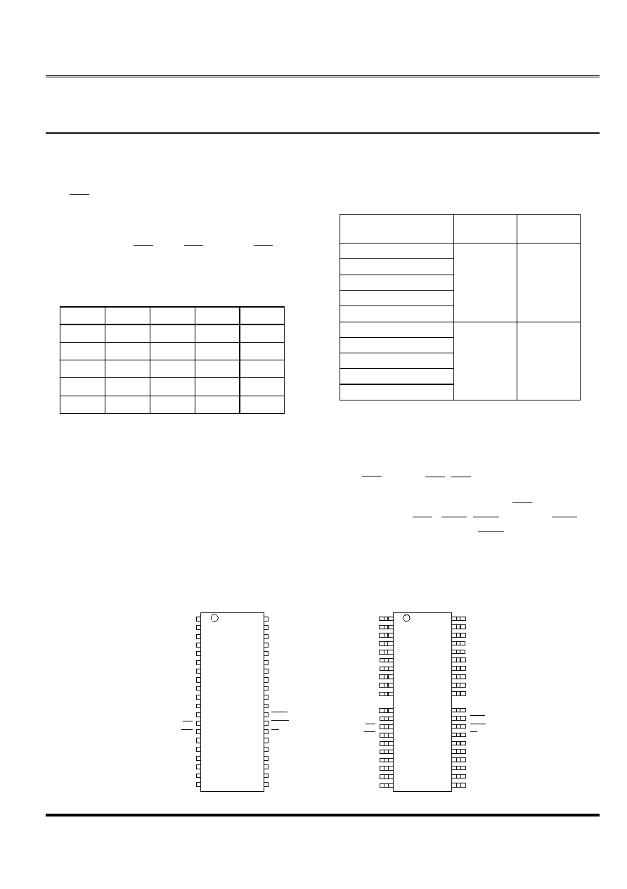
ORDERING INFORMATION - PACKAGE
40-pin 400mil SOJ
44 / 40-pin 400mil TSOP (Type II)
PRODUCT NO.
Refresh
PACKING
TYPE
M11L416256A-25J/T
M11L416256A-28J/T
M11L416256A-30J/T
M11L416256A-35J/T
M11L416256A-40J/T
Normal
SOJ/TSOPII
M11L416256SA-25J/T
M11L416256SA-28J/T
M11L416256SA-30J/T
M11L416256SA-35J/T
M11L416256SA-40J/T
Self-Refresh
SOJ/TSOPII
GENERAL DESCRIPTION
The M11L416256 series is a randomly accessed solid state memory, organized as 262,144 x 16 bits device. It offers
Extended Data-Output , 3.3V(
±
10%) single power supply. Access time (-25,-28,-30,-35,-40) , self-refresh and package type
(SOJ, TSOP II) are optional features of this family. All these family have CAS - before - RAS , RAS -only refresh and Hidden
refresh capabilities.
Two access modes are supported by this device: Byte access and Word access. Use only one of the two CAS and leave
the other staying high will result in a BYTE access. WORD access happens when two CAS ( CASL , CASH ) are used. CASL
transiting low during READ or WRITE cycle will output or input data into the lower byte (IO0~IO7), and CASH transiting low will
output or input data into the upper byte (IO8~15).
PIN ASSIGNMENT
SOJ Top View
TSOP (TypeII) Top View
1
2
3
4
5
6
7
8
9
V
C C
I/O0
I/O1
I/O2
I/O3
V
C C
I/O4
I/O5
I/O6
40
39
38
37
36
35
34
33
32
V
S S
I/O1 5
I/O1 4
I/O1 3
I/O1 2
V
S S
I/O1 1
I/O1 0
I/O9
10
11
12
13
14
15
16
17
18
19
20
I/O7
N C
N C
W E
R A S
N C
A0
A1
A2
A3
V
C C
31
30
29
28
27
26
25
24
23
22
21
I/O8
N C
C A SL
C A S H
OE
A8
A7
A6
A5
A4
V
S S
1
2
3
4
5
6
7
8
9
10
V
C C
I/O 0
I/O 1
I/O 2
I/O 3
V
C C
I/O 4
I/O 5
I/O 6
I/O 7
N C
N C
W E
RA S
N C
A0
A1
A2
A3
V
C C
40
39
38
37
36
35
34
33
32
31
V
S S
I/O 1 5
I/O 1 4
I/O 1 3
I/O 1 2
V
S S
I/O 1 1
I/O 1 0
I/O 9
I/O 8
N C
C AS L
C AS H
O E
A8
A7
A6
A5
A4
V
S S
11
12
13
14
15
16
17
18
19
20
30
29
28
27
26
25
24
23
22
21
(OLWH07
M11L416256A/M11L416256SA
Elite Memory Technology Inc
Publication Date: Agu. 2001
Revision : 1.3 2/16
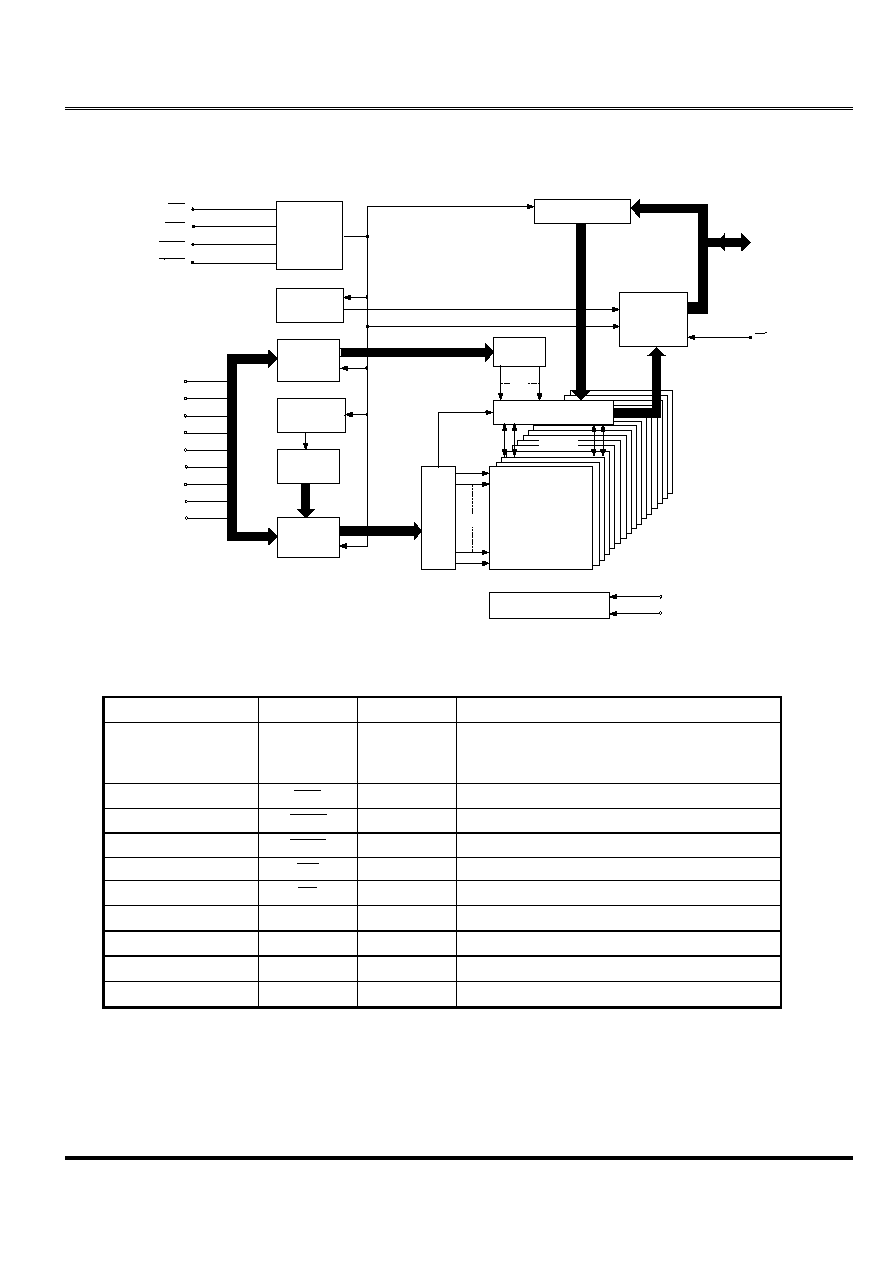
FUNCTIONAL BLOCK DIAGRAM
PIN DESCRIPTIONS
PIN NO.
PIN NAME
TYPE
DESCRIPTION
16~19,22~26
A0~A8
Input
Address Input
Row Address : A0~A8
Column Address : A0~A8
14
RAS
Input
Row Address Strobe
28
CASH
Input
Column Address Strobe / Upper Byte Control
29
CASL
Input
Column Address Strobe / Lower Byte Control
13
WE
Input
Write Enable
27
OE
Input
Output Enable
2~5,7~10,31~34,36~39
I/O0 ~ I/O15
Input / Output Data Input / Output
1,6,20
V
CC
Supply
Power, 3.3V
21,35,40
V
SS
Ground
Ground
11,12,15,30
NC
-
No Connect
CONTROL
LOGIC
DATA-IN BUFFER
CLOCK
GENERATOR
DATA-OUT
BUFFER
COLUMN
ADDRESS
BUFFER
REFRESH
CONTROLER
REFRESH
COUNTER
ROW.
ADDRESS
BUFFERS(9)
9
A0
A1
A2
A3
A4
A5
A6
A7
COLUMN
DECODER
OE
16
R
O
W
DE
CO
DE
R
512 x 512 x 16
MEMORY
ARRAY
16
SENSE AMPLIFIERS
I/O GATING
8
512 x 16
V
CC
V
SS
IO0
:
IO15
RAS
CASH
512
512
9
9
9
9
9
CASL
V
BB
GENERATOR
WE
16
A8
(OLWH07
M11L416256A/M11L416256SA
Elite Memory Technology Inc
Publication Date: Agu. 2001
Revision : 1.3 3/16
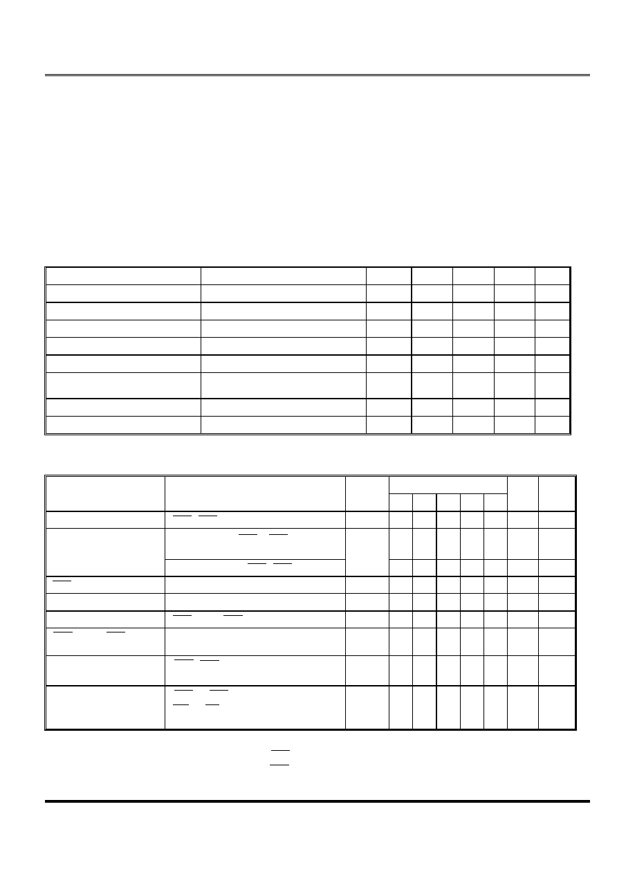
ABSOLUTE MAXIMUM RATINGS
Voltage on Any pin Relative to Vss ... ......-0.5V to +4.6V
Operating Temperature, T
A
(ambient) ....0 C
∞
to +70 C
∞
Storage Temperature (plastic) ..........-55 C
∞
to +150 C
∞
Power Dissipation .......................................0.8W
Short Circuit Output Current ........................50mA
Permanent device damage may occur if "Absolute
Maximum Ratings" are exceeded. This is a stress rating
only, and functional operation of the device above those
conditions indicated in the operational sections of this
specification is not implied. Exposure to absolute
maximum rating conditions for extended periods may
affect reliability.
DC ELECTRICAL CHARACTERISTICS AND RECOMMENDED
OPERATING CONDITIONS
(0 C
∞
T
A
70 C
∞
; V
CC
= 3.3V
±
10% unless otherwise noted)
PARAMETER
CONDITIONS
SYMBOL
MIN
MAX
UNITS NOTES
Supply Voltage
V
CC
3.0
3.6
V
1
Supply Voltage
V
SS
0
0
V
Input High Voltage
V
IH
2.0
V
CC
+0.3
V
1
Input Low Voltage
V
IL
-0.3
0.8
V
1
Input Leakage Current
0V
V
IN
V
IH
(max)
I
LI
-10
10
µ
A
Output Leakage Current
0V
V
OUT
V
CC
Output(s) disable
I
LO
-10
10
µ
A
Output High Voltage
I
OH
= -2 mA
V
OH
2.4
-
V
Output Low Voltage
I
OL
= 2 mA
V
OL
-
0.4
V
Note : 1.All Voltages referenced to V
SS
MAX
PARAMETER
CONDITIONS
SYMBOL
-25
-28
-30
-35
-40
UNITS NOTES
Operating Current
RAS
, CAS cycling , t
RC
=min
I
CC1
210 190 170 150 135
mA
1,2
TTL interface , RAS , CAS = V
IH
,
D
OUT
=High-Z
4
4
4
4
4
mA
Standby Current
CMOS interface, RAS , CAS
V
CC
-0.2V
I
CC2
2
2
2
2
2
mA
RAS
only refresh Current
t
RC
= min
I
CC3
210 190 170 150 135
mA
2
EDO Page Mode Current
t
PC
= min
I
CC4
210 190 170 150 135
mA
1,3
Standby Current
RAS
=V
IH
, CAS = V
IL
I
CC5
5
5
5
5
5
mA
1
CAS
Before RAS Refresh
Current
t
RC
= min
I
CC6
210 190 170 150 135
mA
Battery Backup Current
(S-ver. only)
RAS
, CAS
0.2V, D
OUT
= High-Z,
CMOS interface
I
CC7
400 400 400 400 400
µ
A
Self Refresh Current
(S-ver. only)
RAS
= CAS = V
IL
,
WE = OE = A0~A8 = V
CC
-0.2 or 0.2V
DQ0~DQ15 = V
CC
-0.2, 0.2V or open
I
CC8
400 400 400 400 400
µ
A
Note : 1. I
CC
max is specified at the output open condition.
2. Address can be changed twice or less while RAS =V
IL .
3. Address can be changed once or less while CAS =V
IH
.
(OLWH07
M11L416256A/M11L416256SA
Elite Memory Technology Inc
Publication Date: Agu. 2001
Revision : 1.3 4/16
CAPACITANCE
(Ta = 25 C
∞
, V
CC
= 3.3V
±
10%)
PARAMETER
SYMBOL
TYP
MAX
UNIT
Input Capacitance (address)
C
I1
-
5
pF
Input Capacitance ( RAS , CASH , CASL , WE , OE )
C
I2
-
7
pF
Output capacitance (I/O0~I/O15)
C
I / O
-
10
pF
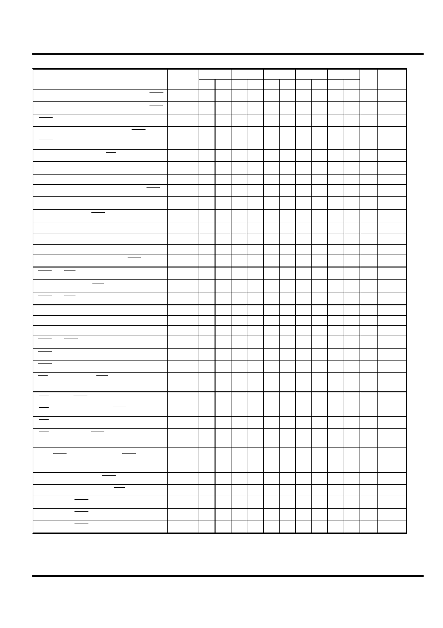
AC ELECTRICAL CHARACTERISTICS
(Ta = 0 to 70 C
∞
, V
CC
=3.3V
±
10%, V
SS
= 0V) (note 14)
Test Conditions
Input timing reference levels : 0.8V, 2.0V
Output reference level : V
OL
= 0.8V, V
OH
=2.0V
Output Load : 2TTL gate + CL (50pF)
Assumed t
T
= 2ns
-25
-28
-30
-35
-40
PARAMETER
SYMBOL
MIN MAX
MIN MAX
MIN MAX MIN MAX
MIN MAX
UNIT NOTES
Read or Write Cycle Time
t
RC
43
48
55
65
75
ns
Read Write Cycle Time
t
RWC
65
70
85
95
105
ns
EDO-Page-Mode Read or Write Cycle
Time
t
PC
10
11
12
14
16
ns
22
EDO-Page-Mode Read-Write Cycle
Time
t
PCM
32
35
37
42
47
ns
22
Access Time From
RAS
t
RAC
25
28
30
35
40
ns
4
Access Time From
CAS
t
CAC
8
9
9
10
11
ns
5,20
Access Time From
OE
t
OAC
8
9
9
10
11
ns
13,20
Access Time From Column Address
t
AA
12
15
15
18
20
ns
Access Time From
CAS
Precharge
t
ACP
14
17
17
20
22
ns
20
RAS
Pulse Width
t
RAS
25
10K
28
10K
30
10K
35
10K
40
10K
ns
RAS
Pulse Width (EDO Page Mode)
t
RASC
25
100K
28
100K
30 100K 35
100K
40 100K
ns
RAS
Hold Time
t
RSH
8
9
9
10
11
ns
25
RAS
Precharge Time
t
RP
15
17
20
25
30
ns
CAS
Pulse Width
t
CAS
4
10K
5
10K
5
10K
5
10K
6
10K
ns
24
CAS
Hold Time
t
CSH
21
24
26
30
35
ns
19
CAS
Precharge Time
t
CP
4
4
4
5
5
ns
6,23
RAS
to
CAS
Delay Time
t
RCD
10
17
10
19
10
21
10
25
10
29
ns
7,18
CAS
to
RAS
Precharge Time
t
CRP
5
5
5
5
5
ns
19
Row Address Setup Time
t
ASR
0
0
0
0
0
ns
Row Address Hold Time
t
RAH
5
5
5
5
5
ns
RAS
to Column Address Delay Time
t
RAD
8
13
8
13
8
15
8
17
8
20
ns
8
Column Address Setup Time
t
ASC
0
0
0
0
0
ns
18
Column Address Hold Time
t
CAH
5
5
5
5
5
ns
18
Column Address Hold Time (Reference
to
RAS
)
t
AR
22
24
26
30
34
ns
Column Address to
RAS
Lead Time
t
RAL
12
15
15
18
20
ns
Read Command Setup Time
t
RCS
0
0
0
0
0
15,18
(OLWH07
M11L416256A/M11L416256SA
Elite Memory Technology Inc
Publication Date: Agu. 2001
Revision : 1.3 5/16
(Continued)
-25
-28
-30
-35
-40
PARAMETER
SYMBOL
MIN MAX MIN MAX MIN MAX MIN MAX MIN MAX
UNIT
NOTES
Read Command Hold Time Reference to
CAS
t
RCH
0
0
0
0
0
ns
9,15,19
Read Command Hold Time Reference to
RAS
t
RRH
0
0
0
0
0
ns
9
CAS
to Output in Low-Z
t
CLZ
3
3
3
3
3
ns
20
Output Buffer Turn-off Delay From
CAS
or
RAS
t
OFF1
3
15
3
15
3
15
3
15
3
15
ns
10,17,20
Output Buffer Turn-off to
OE
t
OFF2
6
7
8
8
8
ns
17,26
Write Command Setup Time
t
WCS
0
0
0
0
0
ns
11,15,18
Write Command Hold Time
t
WCH
5
5
5
5
5
ns
15,25
Write Command Hold Time(Reference to
RAS
)
t
WCR
22
24
26
30
34
ns
15
Write Command Pulse Width
t
WP
5
5
5
5
5
ns
15
Write Command to
RAS
Lead Time
t
RWL
7
7
8
9
10
ns
15
Write Command to
CAS
Lead Time
t
CWL
5
5
6
7
8
ns
15,19
Data-in Setup Time
t
DS
0
0
0
0
0
ns
12,20
Data-in Hold Time
t
DH
5
5
5
5
5
ns
12,20
Data-in Hold Time (Reference to
RAS
)
t
DHR
22
24
26
30
34
ns
RAS
to
WE
Delay Time
t
RWD
34
38
46
51
56
ns
11
Column Address to
WE
Delay Time
t
AWD
21
25
31
34
36
ns
11
CAS
to
WE
Delay Time
t
CWD
17
19
25
26
27
ns
11,18
Transition Time (rise or fall)
t
T
1.5
50
1.5
50
1.5
50
2.5
50
2.5
50
ns
2,3
Refresh Period (512 cycles)
t
REF
8
8
8
8
8
ms
Refresh Period (512 cycles) Self Refresh
t
REF
32
32
32
32
32
ms
RAS
to
CAS
Precharge Time
t
RPC
10
10
10
10
10
ns
CAS
Setup Time(CBR REFRESH)
t
CSR
5
5
10
10
10
ns
1,18
CAS
Hold Time(CBR REFRESH)
t
CHR
7
7
10
10
10
ns
1,19
OE
Hold Time From
WE
During Read-Mode-
Write Cycle
t
OEH
4
4
4
4
5
ns
16
OE
Low to
CAS
High Setup Time
t
OES
4
4
4
4
5
ns
OE
High Hold Time From
CAS
High
t
OEHC
2
2
2
2
2
ns
OE
Precharge Time
t
OEP
2
2
2
2
2
ns
OE
Setup Prior to
RAS
During Hidden Refresh
Cycle
t
ORD
0
0
0
0
0
ns
Last
CAS
Going Low to First
CAS
Returning
High
t
CLCH
4
5
5
5
6
ns
21
Data Output Hold After
CAS
Returning Low
t
COH
3
3
3
3
3
ns
Output Disable Delay From
WE
t
WHZ
3
7
3
7
3
7
3
7
3
7
ns
Self Refresh
RAS
Low Pulse width
t
RASS
100
5
100
100
100
µ
s
27,28
Self Refresh
RAS
High Precharge Time
t
RPS
43
5
55
65
75
ns
27,28
Self Refresh
CAS
Hold Time
t
CHS
-50
-50
-50
-50
-50
ns
27,28