
ESMT
M13L128168A
Elite Semiconductor Memory Technology Inc.
Publication Date : Jun. 2003
Revision : 1.3 1/48
Revision History
Revision 1.3
-Revise operation voltage. (page 5)
Revision 1.2
-Changed t
WTR
from 1 t
CK
to 2 t
CK
.
Revision 1.1
-Changed absolute max. voltage (V
IN
, V
OUT
,V
DD
,V
DDQ
) from 3.6V to 4.0V
Parameter
Symbol
Value
Unit
Voltage on any pin relative to V
SS
V
IN
, V
OUT
-0.5 ~ 4.0
V
Voltage on V
DD
supply relative to V
SS
V
DD
-1.0 ~ 4.0
V
Voltage on V
DDQ
supply relative to V
SS
V
DDQ
-0.5 ~ 4.0
V
-Changed operating VDD from 3.135V~3.6V to 3.135V~3.83V
-Updated DC current specification
Revision 1.0 (21 Oct. 2002)
-No "preliminary" on title.
-Added M13L128168A-3.6T Spec.
-Changed VDDQ from 2.5V � 5% to 2.375V ~ 2.8V
Revision 0.4 (26 Sep. 2002)
-Changed VDD from 3.3V � 5% to 3.135V ~ 3.6V
-Changed operating temperature from 70 C
� to 65 C
�
Revision 0.3 (11 Jul. 2002)
-Added DC Current Spec
Revision 0.2 (29 May. 2002)
-Independent of M13S128168A
Revision 0.1 (3 May. 2002)
-Original

ESMT
M13L128168A
Elite Semiconductor Memory Technology Inc.
Publication Date : Jun. 2003
Revision : 1.3 2/48
DDR SDRAM
2M x 16 Bit x 4 Banks
Double Data Rate SDRAM
Features
JEDEC Standard
Internal pipelined double-data-rate architecture, two data access per clock cycle
Bi-directional data strobe(DQS)
On-chip DLL
Differential clock inputs (CLK and CLK )
DLL aligns DQ and DQS transition with CLK transition
Quad bank operation
CAS Latency : 2, 3
Burst Type : Sequential and Interleave
Burst Length : 2, 4, 8
All inputs except data & DM are sampled at the rising edge of the system clock(CLK)
Data I/O transitions on both edges of data strobe (DQS)
DQS is edge-aligned with data for reads; center-aligned with data for WRITE
LDM/UDM for write masking only
V
DD
= 3.135V-3.83V, V
DDQ
= 2.375V-2.8V
Auto & Self refresh
15.6us refresh interval
1 DQS per byte (LDQS, UDQS)
SSTL-2 I/O interface
66pin TSOPII package
ORDERING INFORMATION:
PRODUCT NO.
MAX. FREQ
V
DD
PACKAGE
M13L128168A-3.6T
276MHz
M13L128168A-4T
250MHz
M13L128168A-5T
200MHz
M13L128168A-6T
166MHz
3.3V
TSOP II
ESMT
M13L128168A
Elite Semiconductor Memory Technology Inc.
Publication Date : Jun. 2003
Revision : 1.3 3/48
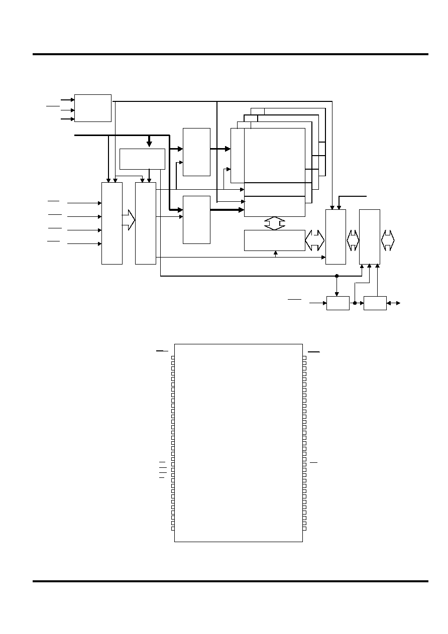
Control Logic
Functional Block Diagram
Pin Arrangement
Bank A
Command Decode
r
Bank D
Latch Circuit
Bank B
Bank C
DM
DQ
Mode Register &
Extended Mode
Register
Column
Address
Buffer
&
Refresh
Counter
Row
Address
Buffer
&
Refresh
Counter
Ro
w
Decode
r
Sense Amplifier
Column Decoder
Data Control Circuit
Input & Out
put
Buf
f
er
Address
Clock
Generator
CLK
CLK
CKE
CS
RAS
CAS
WE
DLL
DQS
CLK, CLK
DQS
1
2
3
4
5
6
7
8
9
10
11
12
13
14
15
16
17
18
19
20
21
22
23
24
25
26
27
28
29
30
31
32
33
66 PIN TSOP(II)
(400mil x 875mil)
(0.65 mm PIN PITCH)
V
DD
DQ
0
V
DDQ
DQ
1
DQ
2
V
SSQ
DQ
3
DQ
4
V
DDQ
DQ
5
DQ
6
V
SSQ
DQ
7
N C
V
DDQ
LDQS
N C
V
DD
N C
LDM
WE
CAS
RAS
CS
N C
BA
0
BA
1
A
10
/AP
A
0
A
1
A
2
A
3
V
DD
V
SS
DQ
15
V
SSQ
DQ
14
DQ
13
V
DDQ
DQ
12
DQ
11
V
SSQ
DQ
10
DQ
9
V
DDQ
DQ
8
N C
V
SSQ
UDQS
N C
V
REF
V
SS
UDM
CLK
CLK
CKE
N C
N C
A
11
A
9
A
8
A
7
A
6
A
5
A
4
V
SS
66
65
64
63
62
61
60
59
58
57
56
55
54
53
52
51
50
49
48
47
46
45
44
43
42
41
40
39
38
37
36
35
34
x16
x16

ESMT
M13L128168A
Elite Semiconductor Memory Technology Inc.
Publication Date : Jun. 2003
Revision : 1.3 4/48
(M13L128168A)
Pin Name
Function
Pin Name
Function
A0~A11,
BA0,BA1
Address inputs
-Row address A0~A11
-Column address A0~A8
A10/AP : AUTO Precharge
BA0, BA1 : Bank selects (4 Banks)
LDM, UDM
DM is an input mask signal for
write data. LDM corresponds to
the data on DQ0~DQ7; UDM
correspond to the data on
DQ8~DQ15.
DQ0~DQ15
Data-in/Data-out
CLK, CLK
Clock input
RAS
Row address strobe
CKE
Clock enable
CAS
Column address strobe
CS
Chip select
WE
Write enable
V
DDQ
Supply Voltage for DQ
V
SS
Ground
V
SSQ
Ground for DQ
V
DD
Power
V
REF
Reference Voltage for SSTL-2
LDQS, UDQS
Bi-directional Data Strobe. LDQS corresponds
to the data on DQ0~DQ7; UDQS correspond to
the data on DQ8~DQ15.
NC
No connection
ESMT
M13L128168A
Elite Semiconductor Memory Technology Inc.
Publication Date : Jun. 2003
Revision : 1.3 5/48
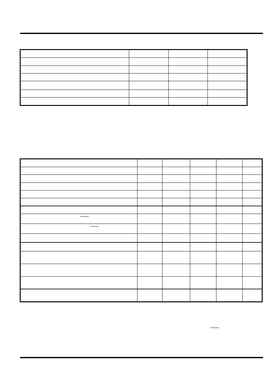
Absolute Maximum Rating
Parameter
Symbol
Value
Unit
Voltage on any pin relative to V
SS
V
IN
, V
OUT
-0.5 ~ 3.6
V
Voltage on V
DD
supply relative to V
SS
V
DD
-1.0 ~ 4.0
V
Voltage on V
DDQ
supply relative to V
SS
V
DDQ
-0.5 ~ 4.0
V
Storage temperature
T
STG
-55 ~ +150
C
�
Power dissipation
P
D
TBD
W
Short circuit current
I
OS
50
mA
Note : Permanent device damage may occur if ABSOLUTE MAXIMUM RATINGS are exceeded.
Functional operation should be restricted to recommend operation condition.
Exposure to higher than recommended voltage for extended periods of time could affect device reliability.
DC Operation Condition & Specifications
DC Operation Condition
Recommended operating conditions (Voltage reference to V
SS
= 0V, T
A
= 0 C
� ~ 65 C
� )
Parameter
Symbol
Min
Max
Unit
Note
Supply voltage
V
DD
3.135
3.6
V
I/O Supply voltage
V
DDQ
2.375
2.8
V
I/O Reference voltage
V
REF
0.49*V
DDQ
0.51*V
DDQ
V
1
I/O Termination voltage (system)
V
TT
V
REF
- 0.04
V
REF
+ 0.04
V
2
Input logic high voltage
V
IH
(DC)
V
REF
+ 0.15
V
DDQ
+ 0.3
V
Input logic low voltage
V
IL
(DC)
-0.3
V
REF
- 0.15
V
Input Voltage Level, CLK and CLK inputs
V
IN
(DC)
-0.3
V
DDQ
+ 0.3
V
Input Differential Voltage, CLK and CLK inputs
V
ID
(DC)
0.36
V
DDQ
+ 0.6
V
Input leakage current
I
I
-5
5
�
A
3
Output leakage current
I
OZ
-5
5
�
A
Output High Current (Normal strength driver)
(V
OUT
= V
TT
+0.76)
I
OH
-15.2
mA
Output Low Current (Normal strength driver)
(V
OUT
= V
TT
-0.76 )
I
OL
+15.2
mA
Output High Current (Weak strength driver)
(V
OUT
= V
TT
+0.45)
I
OH
-9
mA
Output Low Current (Weak strength driver)
(V
OUT
= V
TT
-0.45)
I
OL
+9
mA
Notes 1. V
REF
is expected to be equal to 0.5* V
DDQ
of the transmitting device, and to track variations in the DC level of the same.
Peak-to-peak noise on V
REF
may not exceed 2% of the DC value.
2. V
TT
is not applied directly to the device. V
TT
is system supply for signal termination resistors, is expected to be set equal to
V
REF
, and must track variations in the DC level of V
REF
.
3. V
ID
is the magnitude of the difference between the input level on CLK and the input level on CLK .